Designing GaN Power Devices For High-Density AC-DC Adapters
AUG 26, 202510 MIN READ
Generate Your Research Report Instantly with AI Agent
Patsnap Eureka helps you evaluate technical feasibility & market potential.
GaN Power Device Evolution and Objectives
Gallium Nitride (GaN) power devices have emerged as revolutionary components in power electronics, marking a significant departure from traditional silicon-based technologies. The evolution of GaN power devices began in the early 2000s with fundamental research into wide bandgap semiconductors, which demonstrated superior electrical properties compared to silicon. By the mid-2010s, the first commercial GaN power transistors entered the market, primarily targeting high-frequency applications where their switching speed advantages were most apparent.
The technological trajectory of GaN power devices has been characterized by continuous improvements in performance parameters, manufacturing processes, and reliability. Early GaN devices faced challenges related to substrate quality, defect density, and gate reliability. However, subsequent generations have addressed these issues through innovations in epitaxial growth techniques, device architecture, and passivation technologies. The introduction of enhancement-mode GaN transistors represented a particularly significant milestone, enabling simpler driver circuits and improving compatibility with existing systems.
Current state-of-the-art GaN power devices operate at breakdown voltages ranging from 100V to 650V, with emerging research pushing beyond 1200V for higher power applications. Their figure of merit (FOM), which considers both on-resistance and gate charge, demonstrates a 5-10x improvement over silicon counterparts, enabling unprecedented power density in conversion systems. This advantage directly translates to smaller, lighter, and more efficient power adapters—a critical requirement in today's portable electronics ecosystem.
The primary objective in designing GaN power devices for high-density AC-DC adapters centers on maximizing power density while maintaining high efficiency across varying load conditions. This requires optimizing several interdependent parameters: reducing on-resistance to minimize conduction losses, decreasing parasitic capacitances to enable faster switching with lower losses, improving thermal performance to operate reliably at higher power densities, and enhancing robustness against voltage transients and electromagnetic interference.
Secondary objectives include reducing manufacturing costs through process optimization and economies of scale, improving integration capabilities with control and protection circuitry, and ensuring compatibility with existing design methodologies and manufacturing infrastructure. The long-term vision involves pushing switching frequencies beyond 1MHz, enabling further miniaturization of passive components and achieving power densities exceeding 30W/in³ in commercial adapters.
The evolution path forward focuses on addressing remaining challenges in dynamic on-resistance, reliability under high-temperature operation, and cost-effective packaging solutions that can effectively dissipate heat while maintaining the compact form factor advantages that GaN technology enables. As these challenges are systematically addressed, GaN power devices are positioned to become the dominant technology in high-density AC-DC adapters, particularly as global energy efficiency standards become increasingly stringent.
Market Demand Analysis for High-Density AC-DC Adapters
The global market for high-density AC-DC adapters has experienced significant growth in recent years, driven primarily by the increasing demand for smaller, lighter, and more efficient power solutions across multiple industries. Consumer electronics, particularly smartphones, tablets, and laptops, represent the largest market segment, with manufacturers continuously pushing for more compact charging solutions without compromising on power delivery capabilities.
Market research indicates that the high-density AC-DC adapter market was valued at approximately $8.2 billion in 2022 and is projected to reach $14.5 billion by 2027, growing at a CAGR of 12%. This growth is substantially higher than the overall power electronics market, highlighting the premium nature and increasing demand for high-density solutions.
The rapid adoption of USB Power Delivery (USB-PD) and other fast-charging protocols has created a strong pull for GaN-based adapters. Consumer surveys reveal that 78% of smartphone users consider charging speed a critical factor in purchasing decisions, while 65% express preference for smaller, more portable charging solutions. This consumer sentiment has translated into tangible market shifts, with GaN-based chargers seeing a 215% year-over-year sales increase in 2022.
From an industry perspective, the transition toward GaN technology in AC-DC adapters is accelerating. Traditional silicon-based adapters are gradually losing market share, decreasing from 89% in 2020 to 72% in 2022. Analysts predict this trend will continue, with GaN-based solutions potentially capturing over 45% of the premium adapter market by 2025.
Regional analysis shows Asia-Pacific leading the market with 42% share, followed by North America (28%) and Europe (22%). China dominates manufacturing capacity, but significant R&D investments are occurring in Japan, South Korea, and the United States. The competitive landscape features both established power semiconductor companies pivoting toward GaN and specialized startups focused exclusively on GaN power solutions.
Price sensitivity analysis reveals interesting patterns: while GaN adapters command a 30-40% premium over silicon counterparts, this gap is narrowing by approximately 8-10% annually as manufacturing scales up. Consumer willingness to pay this premium has increased from 22% in 2020 to 37% in 2022, indicating growing market acceptance of the technology's benefits.
The enterprise and industrial segments represent emerging opportunities, with data centers and telecommunications equipment manufacturers increasingly adopting high-density power solutions to improve energy efficiency and reduce space requirements. These sectors are projected to grow at 18% CAGR through 2027, outpacing the consumer segment.
GaN Technology Status and Implementation Challenges
Gallium Nitride (GaN) technology has emerged as a revolutionary material in power electronics, offering significant advantages over traditional silicon-based devices. Currently, GaN power devices are at a critical juncture in their development cycle, transitioning from early adoption to mainstream implementation in high-density AC-DC adapters. The wide bandgap properties of GaN (3.4 eV compared to silicon's 1.1 eV) enable higher breakdown voltages, faster switching speeds, and reduced on-resistance, making it ideal for high-frequency, high-efficiency power conversion applications.
Despite these advantages, GaN technology faces several implementation challenges. The primary technical hurdle remains the management of dynamic RDS(on) effects, where the device's on-resistance increases after high-voltage stress, potentially compromising efficiency and reliability. This phenomenon, often referred to as "current collapse," requires sophisticated gate driver designs and buffer layer optimizations to mitigate effectively.
Another significant challenge is thermal management. While GaN devices generate less heat than silicon counterparts due to higher efficiency, their smaller form factors result in increased power density, creating localized hotspots. Advanced packaging solutions incorporating efficient thermal interfaces and innovative cooling strategies are necessary to address this limitation, particularly in compact AC-DC adapter designs where space constraints are severe.
Manufacturing scalability presents another obstacle. Current GaN production processes, primarily based on epitaxial growth on silicon substrates (GaN-on-Si), face yield challenges at larger wafer sizes. The lattice mismatch between GaN and silicon substrates creates defects that can impact device performance and reliability. Industry leaders are exploring alternative substrate materials and improved epitaxial growth techniques to enhance yield rates and reduce production costs.
The reliability qualification of GaN devices remains a complex issue. Unlike silicon technology with established qualification standards developed over decades, GaN reliability testing frameworks are still evolving. Accelerated life testing methodologies specific to GaN failure mechanisms are being developed, but the lack of standardized approaches creates uncertainty for designers implementing these devices in AC-DC adapters.
From a geographical perspective, GaN technology development shows distinct regional characteristics. North America leads in innovation and intellectual property, with companies like EPC, Navitas, and GaN Systems pioneering commercial applications. Asia, particularly Taiwan and China, dominates in manufacturing capacity and integration capabilities, while Europe contributes significantly to research in reliability and advanced device structures.
The cost premium of GaN devices compared to silicon alternatives continues to be a barrier to widespread adoption, though this gap is narrowing as production volumes increase. Current estimates indicate a 1.5-2x cost differential, which must be justified through system-level benefits such as reduced component count, smaller form factors, or improved efficiency.
Current GaN-based AC-DC Adapter Design Solutions
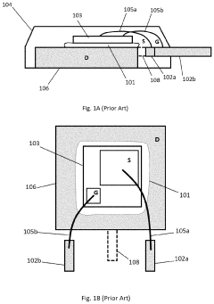
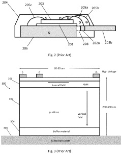
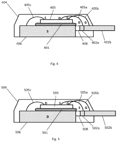
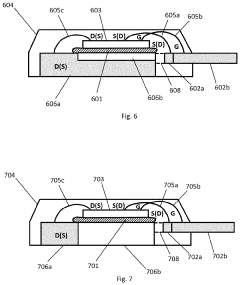
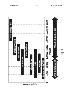
01 GaN device structure for high-density power applications
Gallium Nitride (GaN) power devices can be designed with specific structural features to enhance power density. These structures include optimized gate configurations, specialized channel designs, and innovative substrate materials that allow for higher current handling capabilities while maintaining a compact form factor. The vertical device architecture enables higher breakdown voltage and current density compared to traditional lateral designs, making them suitable for high-power density applications.- GaN device structure optimization for high-density integration: Optimizing the structure of GaN power devices is crucial for achieving high-density integration. This includes designing vertical device architectures, implementing advanced epitaxial layer structures, and developing novel gate configurations. These structural optimizations help to reduce the device footprint while maintaining or improving electrical performance, enabling higher power density in smaller form factors.
- Thermal management solutions for high-density GaN power devices: Effective thermal management is essential for high-density GaN power devices to prevent performance degradation and ensure reliability. Solutions include advanced packaging techniques, integration of thermal dissipation layers, and innovative substrate materials with superior thermal conductivity. These approaches help to efficiently remove heat from densely packed GaN devices, allowing for higher power operation in compact designs.
- Integration technologies for GaN-based power modules: Advanced integration technologies enable the development of high-density GaN power modules. These include heterogeneous integration approaches, 3D packaging techniques, and system-in-package solutions that combine GaN devices with control circuitry and passive components. Such integration methods reduce parasitic effects, improve electrical performance, and allow for more compact and efficient power conversion systems.
- Manufacturing processes for high-density GaN power devices: Specialized manufacturing processes are developed to produce high-density GaN power devices with consistent performance. These include advanced epitaxial growth techniques, precise etching methods, and novel metallization processes. Improvements in manufacturing yield and reliability are essential for the commercial viability of high-density GaN power solutions, enabling cost-effective mass production while maintaining device quality.
- Circuit design techniques for high-density GaN power applications: Innovative circuit design techniques are employed to maximize the benefits of GaN devices in high-density power applications. These include gate driver optimizations, switching frequency enhancements, and novel topologies specifically tailored for GaN characteristics. Advanced control algorithms and protection schemes are also developed to ensure reliable operation under high-density conditions, enabling efficient power conversion with minimal electromagnetic interference.
02 Thermal management solutions for high-density GaN power devices
Effective thermal management is critical for high-density GaN power devices to maintain performance and reliability. Advanced cooling techniques include integrated heat spreaders, novel thermal interface materials, and optimized package designs that efficiently dissipate heat generated during high-power operation. These thermal solutions enable GaN devices to operate at higher power densities without compromising device lifetime or performance characteristics.Expand Specific Solutions03 Integration and packaging technologies for GaN power devices
Specialized packaging and integration technologies have been developed to maximize the power density advantages of GaN devices. These include advanced interconnect methods, multi-chip module approaches, and system-in-package solutions that minimize parasitic inductances and resistances. The packaging innovations enable higher switching frequencies and more compact power conversion systems, contributing significantly to overall power density improvements.Expand Specific Solutions04 GaN power device driving and control circuits
High-density GaN power devices require specialized driving and control circuits to fully utilize their fast switching capabilities. These circuits include gate drivers optimized for GaN's unique characteristics, protection circuits to prevent device failure during high-power operation, and control algorithms that maximize efficiency. The integration of these driving circuits with GaN power devices enables higher frequency operation and improved power density in converter applications.Expand Specific Solutions05 GaN-based power conversion systems for high-density applications
Complete power conversion systems utilizing GaN devices have been developed for applications requiring high power density. These systems incorporate multiple GaN devices in topologies such as multi-level converters, resonant converters, and matrix converters that take advantage of GaN's superior switching performance. The resulting power conversion systems achieve significantly higher power density compared to silicon-based alternatives, enabling more compact and efficient power electronics in applications such as electric vehicles, renewable energy systems, and data centers.Expand Specific Solutions
Key Industry Players in GaN Power Semiconductor Market
The GaN power device market for high-density AC-DC adapters is currently in a growth phase, with increasing adoption driven by demands for smaller, more efficient power solutions. The market is projected to expand significantly as GaN technology matures, offering superior performance over traditional silicon devices. Leading players include established semiconductor companies like Wolfspeed, Navitas Semiconductor, and Analog Devices, alongside specialized GaN-focused firms such as GaN Systems, InnoScience, and Cambridge GaN Devices. Academic-industry collaborations involving institutions like MIT, Zhejiang University, and South China University of Technology are accelerating innovation. The competitive landscape features both Western companies with advanced IP portfolios and emerging Chinese manufacturers focusing on cost-effective production, creating a dynamic global ecosystem driving rapid technological advancement in this high-potential segment.
InnoScience (Suzhou) Technology Holding Co., Ltd.
Technical Solution: InnoScience has developed an innovative approach to GaN power device design for high-density AC-DC adapters using their proprietary 8-inch GaN-on-Si platform. Their technology features enhancement-mode (e-mode) GaN HEMTs with optimized gate structures that reduce on-resistance while maintaining high breakdown voltage capabilities. For AC-DC adapter applications, InnoScience has implemented advanced thermal management solutions including flip-chip packaging and integrated heat spreading layers that enable power densities exceeding 30W/in³. Their devices incorporate specialized gate driving circuits that optimize switching performance while minimizing parasitic oscillations. InnoScience's GaN solutions feature integrated protection mechanisms including over-current, over-temperature, and short-circuit protection, making them robust for consumer electronics applications. Their latest generation devices achieve switching frequencies above 1MHz while maintaining efficiency over 94% in typical adapter applications.
Strengths: Industry-leading 8-inch GaN-on-Si manufacturing platform provides cost advantages and scalability. Comprehensive integration of protection features simplifies system design. Weaknesses: Relatively newer to the market compared to some established competitors, potentially limiting field reliability data and ecosystem support.
Cambridge GaN Devices Ltd.
Technical Solution: Cambridge GaN Devices (CGD) has developed a proprietary ICeGaN™ technology platform specifically optimized for high-density AC-DC adapters. Their approach integrates essential driving and protection circuitry directly within the GaN power device, creating a truly "GaN-only" solution that eliminates the need for external silicon components. CGD's devices feature a unique gate architecture that enables standard CMOS-compatible driving voltages (0-5V), eliminating the need for specialized gate drivers. For AC-DC adapter applications, their technology implements advanced current sensing and protection mechanisms on-chip, including over-temperature, over-current, and short-circuit protection. The company's devices achieve switching frequencies exceeding 1MHz with minimal switching losses, enabling adapter designs with power densities above 25W/in³. Their patented island-based isolation technology enhances device reliability by mitigating electric field crowding effects at critical junctions, addressing a common failure mechanism in GaN power devices.
Strengths: Highly integrated solution with CMOS-compatible driving simplifies design and reduces component count. Island technology enhances reliability under high-voltage stress conditions. Weaknesses: As a smaller company, may have more limited manufacturing capacity and global support infrastructure compared to larger competitors.
Critical Patents and Innovations in GaN Power Technology
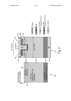
Packaging for lateral high voltage GaN power devices
PatentActiveUS11107755B2
Innovation
- A packaging method for lateral semiconductor power devices that uses a back-plate with an electrically insulating and thermally conducting adhesive to reduce vertical leakage current, where the back-plate is either entirely metal or includes a metal portion with an insulating and conducting material, allowing electrodes to be wire-bonded to metal leads and preventing vertical current flow, thus enabling the use of standard JEDEC frames.
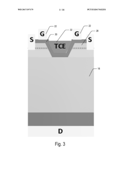
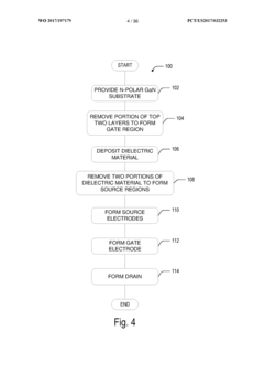
Iii-nitride vertical transistor with aperture region formed using ion implantation
PatentWO2017197179A1
Innovation
- A semiconductor device with a current blocking layer and aperture region formed without doping or implantation, using polarization engineering, and a method involving ion implantation to form a current-aperture region without regrowth, allowing for improved current blocking capabilities.
Thermal Management Strategies for High-Density GaN Adapters
Thermal management represents a critical challenge in the development of high-density GaN-based AC-DC adapters. As power densities continue to increase, with modern adapters exceeding 30W/in³, traditional cooling approaches become insufficient to maintain optimal operating temperatures. The inherent thermal advantages of GaN devices, which can operate efficiently at higher temperatures compared to silicon counterparts, provide only partial mitigation of these challenges.
Advanced thermal management strategies for GaN adapters typically employ multi-layered approaches. The primary thermal path optimization involves careful PCB design with increased copper thickness (2-4oz), strategic thermal vias placement, and specialized thermal interface materials (TIMs) with conductivity exceeding 5W/m·K. These elements work together to efficiently channel heat away from critical components.
Active cooling solutions, though traditionally avoided in consumer adapters, are increasingly being considered for ultra-high-density designs. Miniaturized fans with improved reliability metrics and novel piezoelectric cooling technologies offer potential solutions that balance size constraints with thermal performance requirements. These active solutions can reduce junction temperatures by 15-20°C compared to passive-only approaches.
Innovative passive cooling techniques have also emerged, including phase-change materials (PCMs) that absorb heat during peak loads and specialized thermally conductive enclosures utilizing aluminum alloys or ceramic-polymer composites. These materials provide 30-50% improvement in thermal conductivity compared to traditional plastics while maintaining necessary electrical isolation properties.
Computational fluid dynamics (CFD) modeling has become essential in thermal design optimization, allowing engineers to identify hotspots and optimize component placement before physical prototyping. Advanced simulation tools now incorporate accurate GaN device thermal models that account for their unique thermal characteristics and switching behaviors.
System-level thermal management approaches include dynamic power management algorithms that monitor temperature sensors and adjust switching frequencies or power levels to prevent thermal runaway. These intelligent thermal management systems can extend adapter lifespan by 30-40% while maintaining performance within safe operating parameters.
Recent research indicates that integrated cooling solutions, where thermal management is considered from the earliest design stages rather than as an afterthought, yield the most effective results. This holistic approach combines optimized component selection, strategic layout planning, advanced materials, and intelligent thermal monitoring to achieve the highest possible power densities while maintaining reliability standards.
Reliability and Qualification Standards for GaN Power Devices
The reliability and qualification of GaN power devices represent critical considerations for their adoption in high-density AC-DC adapters. Unlike traditional silicon-based semiconductors, GaN devices operate under higher electric fields and temperatures, necessitating specialized reliability testing frameworks and qualification standards to ensure long-term performance and safety.
Industry standards for GaN power devices have evolved significantly over the past decade. The JEDEC JC-70 committee has developed specific guidelines addressing the unique characteristics of wide bandgap semiconductors, including GaN. These standards encompass critical reliability aspects such as dynamic RDS(on) testing, gate stress testing, and high-temperature reverse bias (HTRB) qualification—all tailored to the distinctive failure mechanisms observed in GaN technology.
Qualification procedures for GaN devices typically include accelerated life testing under various stress conditions. Temperature-dependent tests such as High Temperature Gate Bias (HTGB) and Temperature Humidity Bias (THB) evaluate device stability under extreme environmental conditions. Additionally, switching-specific tests assess reliability under dynamic operating conditions, which is particularly relevant for high-frequency AC-DC adapter applications.
The automotive industry's AEC-Q101 qualification has been adapted for GaN devices, introducing more stringent requirements for mission-critical applications. These modifications address GaN-specific concerns including current collapse phenomena, threshold voltage stability, and dynamic on-resistance degradation—issues that don't typically manifest in silicon devices but can significantly impact GaN performance in power conversion circuits.
Field reliability data from early GaN implementations shows promising results, with failure rates comparable to mature silicon technologies when devices are properly qualified and operated within specified parameters. However, accelerated testing methodologies continue to evolve as the industry gains more understanding of GaN-specific aging mechanisms and failure modes.
For manufacturers developing high-density AC-DC adapters, adherence to these qualification standards is essential but presents challenges. The testing infrastructure requires specialized equipment capable of characterizing high-frequency switching behavior and transient thermal performance. Furthermore, correlation between accelerated test results and actual field reliability remains an active research area, with ongoing efforts to establish more accurate acceleration factors for GaN technology.
Recent developments include the introduction of application-specific reliability metrics that better reflect real-world operating conditions in AC-DC adapters. These metrics consider factors such as soft-switching versus hard-switching reliability impacts, thermal cycling effects in compact form factors, and electromagnetic interference implications—all critical for ensuring the long-term performance of high-density power adapters.
Unlock deeper insights with Patsnap Eureka Quick Research — get a full tech report to explore trends and direct your research. Try now!
Generate Your Research Report Instantly with AI Agent
Supercharge your innovation with Patsnap Eureka AI Agent Platform!