Gate Drive Strategies For GaN Power Devices: Isolation, Miller, And Protection
AUG 26, 20259 MIN READ
Generate Your Research Report Instantly with AI Agent
Patsnap Eureka helps you evaluate technical feasibility & market potential.
GaN Power Device Evolution and Objectives
Gallium Nitride (GaN) power devices have emerged as revolutionary components in power electronics, offering significant advantages over traditional silicon-based semiconductors. The evolution of GaN technology began in the early 1990s with fundamental research into wide bandgap materials, but commercial viability was only achieved in the 2010s after overcoming numerous material science and manufacturing challenges.
The initial development focused on lateral GaN high-electron-mobility transistors (HEMTs), which leveraged the two-dimensional electron gas (2DEG) formed at the AlGaN/GaN heterojunction. This unique property enabled devices with exceptionally low on-resistance and high switching speeds. By 2010, enhancement-mode GaN transistors began entering the market, eliminating the need for negative gate drive voltages that complicated early depletion-mode designs.
A significant milestone occurred around 2015 when GaN-on-Si technology matured, allowing GaN devices to be manufactured on standard silicon substrates. This breakthrough dramatically reduced production costs and accelerated market adoption. Subsequently, integration capabilities improved, enabling monolithic integration of gate drivers with GaN power devices, which addressed many of the gate drive challenges inherent to these high-speed switches.
The technical objectives for GaN power devices center on several key areas. First is the optimization of gate drive strategies to fully exploit GaN's switching speed potential while maintaining reliability. This includes developing isolation techniques that can withstand the extreme dv/dt rates (often exceeding 100V/ns) without compromising signal integrity or introducing parasitic effects.
Another critical objective is addressing the Miller effect, which poses significant challenges in GaN applications due to the devices' extremely fast switching transitions. Effective Miller clamping techniques are essential to prevent false turn-on events that can lead to catastrophic shoot-through failures in half-bridge configurations.
Protection mechanisms represent another vital development goal, as GaN devices have different failure modes compared to silicon MOSFETs. These include implementing robust overvoltage, overcurrent, and overtemperature protection schemes that can respond within nanoseconds to prevent device damage.
Looking forward, the industry aims to push GaN operating voltages beyond the current 650V ceiling toward 1200V and higher, enabling applications in electric vehicle traction inverters and renewable energy systems. Simultaneously, there are efforts to further reduce gate drive complexity while enhancing immunity to noise and parasitic effects, which would simplify system design and improve reliability in harsh electromagnetic environments.
Market Demand Analysis for GaN Gate Drive Solutions
The global market for GaN power devices is experiencing robust growth, driven by increasing demand for high-efficiency power conversion systems across multiple industries. The compound annual growth rate (CAGR) for GaN power devices is projected to exceed 20% through 2028, with the gate drive solutions segment representing a critical component of this expansion. This growth trajectory is creating substantial market opportunities for specialized gate drive solutions that can effectively address the unique requirements of GaN technology.
The automotive sector represents one of the most significant market drivers, particularly with the rapid adoption of electric vehicles (EVs). The EV charging infrastructure market alone is expected to grow substantially, requiring high-efficiency power conversion systems where GaN excels. Additionally, the renewable energy sector's expansion has created increased demand for efficient power conversion in solar inverters and wind power systems, where GaN-based solutions offer superior performance compared to traditional silicon-based alternatives.
Consumer electronics manufacturers are increasingly adopting GaN technology for fast chargers and power adapters, creating a high-volume market for compact gate drive solutions. This trend is particularly evident in the smartphone and laptop segments, where manufacturers compete on charging speed and adapter size. The data center industry also represents a substantial market opportunity, with operators seeking to improve power density and efficiency in server power supplies to reduce operational costs and carbon footprint.
Industrial automation systems are another key market segment, where the precise control capabilities offered by advanced gate drive solutions enable more efficient motor drives and power conversion systems. The telecommunications infrastructure market, particularly with the ongoing 5G rollout, requires compact, efficient power solutions where GaN technology provides significant advantages over traditional approaches.
Regional analysis indicates that Asia-Pacific currently dominates the market demand, with China, Japan, South Korea, and Taiwan being major manufacturing hubs for GaN power devices and associated gate drive solutions. North America and Europe follow closely, driven by automotive and renewable energy applications respectively.
Market research indicates that customers are primarily seeking gate drive solutions that offer superior isolation capabilities to handle the higher switching speeds of GaN, effective Miller effect mitigation to prevent false triggering, and robust protection features to safeguard these relatively expensive power devices. Additionally, there is growing demand for integrated solutions that reduce component count and simplify design implementation, particularly among smaller OEMs with limited GaN design experience.
Technical Challenges in GaN Gate Drive Implementation
The implementation of gate drive circuits for Gallium Nitride (GaN) power devices presents several significant technical challenges that must be addressed to fully leverage the superior performance capabilities of these wide bandgap semiconductors. Unlike traditional silicon-based power devices, GaN transistors operate at much higher switching frequencies and exhibit unique characteristics that demand specialized gate drive solutions.
One primary challenge is the stringent gate voltage requirements of GaN devices. These transistors typically have a narrower safe operating gate voltage range compared to silicon MOSFETs, with maximum gate-source voltage ratings often limited to 6-7V. Exceeding these limits, even transiently, can lead to permanent device damage. This necessitates precise voltage regulation and protection mechanisms within the gate driver circuit to prevent overvoltage conditions during both steady-state operation and transient events.
The extremely fast switching speeds of GaN devices, while advantageous for efficiency, create significant challenges for gate drive design. Switching transitions can occur in sub-nanosecond timeframes, requiring gate drivers with exceptional bandwidth and minimal propagation delays. These rapid transitions generate substantial dv/dt and di/dt rates that can induce parasitic turn-on through the Miller capacitance, potentially leading to shoot-through conditions and catastrophic device failure.
Common-mode transient immunity (CMTI) represents another critical challenge, particularly in half-bridge and bridge configurations. The high dv/dt rates during switching can couple through isolation barriers and parasitic capacitances, causing false triggering or disruption of control signals. Gate drivers must therefore incorporate robust isolation technologies and circuit techniques to maintain signal integrity under these extreme operating conditions.
Thermal management presents additional complications, as GaN gate drivers must often be positioned in close proximity to the power devices to minimize loop inductances. This placement exposes the driver circuitry to elevated temperatures, necessitating components with extended temperature ratings and careful thermal design considerations.
Layout and packaging constraints further complicate GaN gate drive implementation. The need to minimize parasitic inductances in the gate drive loop requires extremely compact designs with optimized current return paths. This often conflicts with isolation requirements and thermal management needs, creating complex design trade-offs.
Finally, protection mechanisms for GaN devices must operate at significantly faster timescales than traditional silicon-based systems. Conventional overcurrent protection schemes may be too slow to prevent damage during fault conditions, requiring innovative approaches such as active Miller clamping, desaturation detection modifications, and advanced soft-shutdown techniques specifically tailored to the unique characteristics of GaN power devices.
Current Gate Drive Isolation and Protection Strategies
01 Gate driver circuit design for GaN power devices
Specialized gate driver circuits are designed for GaN power devices to address their unique switching characteristics. These circuits typically include features like precise voltage control, optimized turn-on and turn-off paths, and protection mechanisms to prevent gate overvoltage. The design focuses on achieving high switching speeds while maintaining reliability and preventing parasitic oscillations that can occur with GaN devices.- Gate driver circuit design for GaN power devices: Specialized gate driver circuits are designed for GaN power devices to address their unique switching characteristics. These circuits typically include features like precise voltage control, optimized turn-on/turn-off timing, and protection mechanisms to prevent gate overvoltage. The design focuses on minimizing parasitic inductances and providing clean switching signals to maximize the high-speed performance advantages of GaN technology.
- Integration and packaging solutions for GaN gate drivers: Advanced packaging and integration techniques are employed to optimize the performance of GaN gate drivers. These solutions include co-packaging of driver and power device, embedded gate driver structures, and specialized interconnect technologies that minimize parasitic elements. The integration approaches focus on reducing loop inductance, improving thermal management, and enhancing overall switching performance while maintaining reliability.
- Protection mechanisms for GaN gate drivers: Protection circuits and mechanisms are implemented in GaN gate drivers to prevent device failure during operation. These include overcurrent protection, overvoltage protection, short-circuit protection, and temperature monitoring. The protection schemes are designed to respond quickly to fault conditions, considering the high switching speeds of GaN devices, and to ensure safe operation across various operating conditions.
- Multi-level and advanced driving techniques for GaN devices: Advanced driving techniques are developed for GaN power devices to optimize their performance. These include multi-level driving schemes, adaptive gate driving, resonant gate driving, and current-mode driving. These techniques aim to reduce switching losses, improve efficiency, enable higher switching frequencies, and enhance the overall performance of GaN-based power conversion systems.
- Temperature and voltage compensation in GaN gate drivers: Compensation techniques are implemented in GaN gate drivers to maintain optimal performance across varying operating conditions. These include temperature compensation circuits that adjust gate drive parameters based on device temperature, and voltage compensation mechanisms that adapt to changes in supply voltage or load conditions. These compensation methods ensure consistent switching behavior and reliability of GaN power devices in dynamic operating environments.
02 Integration of gate drivers with GaN power devices
Integration approaches combine GaN power devices with gate driver circuits in compact packages or on the same substrate. This integration reduces parasitic inductances, improves switching performance, and enhances thermal management. Monolithic or hybrid integration techniques are employed to create more efficient power modules with reduced footprint and improved electromagnetic interference (EMI) characteristics.Expand Specific Solutions03 Protection mechanisms for GaN gate drivers
Specialized protection circuits are implemented in GaN gate drivers to prevent device failure during operation. These include over-current protection, over-voltage protection, and temperature monitoring systems. The protection mechanisms are designed to respond quickly to fault conditions, preventing damage to the sensitive gate structure of GaN devices while maintaining the high-speed switching capabilities that make GaN technology advantageous.Expand Specific Solutions04 Isolated gate drive solutions for GaN devices
Isolation technologies are implemented in GaN gate drivers to separate control circuitry from high-voltage power stages. These solutions use techniques such as optical isolation, magnetic isolation, or capacitive coupling to transfer gate signals while maintaining voltage isolation. Isolated gate drivers are particularly important in high-voltage applications and bridge configurations where multiple GaN devices operate at different reference potentials.Expand Specific Solutions05 Advanced control strategies for GaN gate drivers
Sophisticated control algorithms and techniques are employed in GaN gate drivers to optimize switching performance. These include adaptive gate driving, variable slew rate control, and dead-time optimization. The control strategies aim to balance switching losses, electromagnetic interference, and reliability concerns while taking advantage of the high-speed capabilities of GaN power devices. Some implementations incorporate digital control for greater flexibility and precision.Expand Specific Solutions
Key Industry Players in GaN Power Electronics
The GaN power device gate drive technology market is in a growth phase, with increasing adoption across consumer electronics, automotive, and renewable energy sectors. The market is projected to expand significantly due to GaN's superior performance over silicon in high-frequency, high-power applications. Leading companies like GaN Systems, Navitas Semiconductor, and Efficient Power Conversion are driving innovation in isolation techniques, Miller effect mitigation, and protection circuits. Academic institutions including UESTC and HKUST are collaborating with industry players such as Huawei and STMicroelectronics to advance gate drive technology maturity. The competitive landscape features established semiconductor manufacturers and specialized GaN startups developing integrated solutions to address the unique challenges of GaN switching characteristics, with technology maturity advancing from research to commercial implementation.
GaN Systems, Inc.
Technical Solution: GaN Systems开发了专有的栅极驱动解决方案,专为其增强型GaN HEMT器件优化。其技术方案包括集成隔离技术的驱动器设计,采用变压器或数字隔离器实现高压隔离,同时提供高共模瞬态抑制能力。针对米勒效应,GaN Systems实现了主动钳位技术,通过精确控制栅极电压摆率和添加外部钳位电路,有效抑制寄生开关。其保护策略包括过流、过压和过温保护,采用快速响应电路(<100ns)检测异常并触发保护机制。GaN Systems还开发了专用的GateDrive Plus技术,集成了驱动和保护功能,可实现高达100V/ns的开关速率,同时保持低EMI特性[1][3]。
优势:专为GaN器件优化的驱动解决方案,提供业界领先的开关速度和效率;集成保护功能减少外部组件需求;提供完整的参考设计加速客户产品开发。劣势:相比硅基解决方案初始成本较高;对PCB布局和系统设计要求严格,增加了设计复杂性。
STMicroelectronics International NV
Technical Solution: ST开发了STGAP系列专用GaN栅极驱动器,采用先进的BCD工艺和专有隔离技术。其技术方案包括集成式电容隔离架构,提供高达200kV/μs的共模瞬态抑制能力和低于50ns的传播延迟。针对米勒效应,ST实现了主动钳位技术和精确的死区时间控制,通过独立的源极和漏极路径驱动,有效防止寄生开通。保护策略方面,ST集成了多级保护机制,包括可编程UVLO、过流保护和热关断功能。其STGAP2S系列产品支持负关断电压,确保GaN器件在高频应用中的可靠关断。ST还开发了MasterGaN系列集成产品,将GaN功率级、驱动器和控制器集成在单个封装中,简化系统设计。最新一代产品集成了数字接口,支持通过SPI总线进行实时监控和参数调整,提高系统灵活性和可靠性[9][11]。ST的解决方案广泛应用于电动车充电、数据中心电源和工业驱动等领域。
优势:提供从驱动器到完整电源解决方案的全面产品组合;强大的应用支持和参考设计;与ST微控制器和模拟产品高度兼容,形成完整生态系统。劣势:某些高级功能需要复杂的外部电路;在超高频应用(>5MHz)性能不如某些专业GaN公司;部分解决方案针对特定应用优化,通用性受限。
Miller Effect Mitigation Techniques and Patents
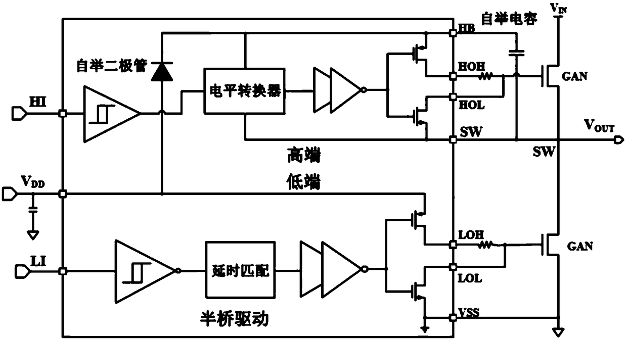
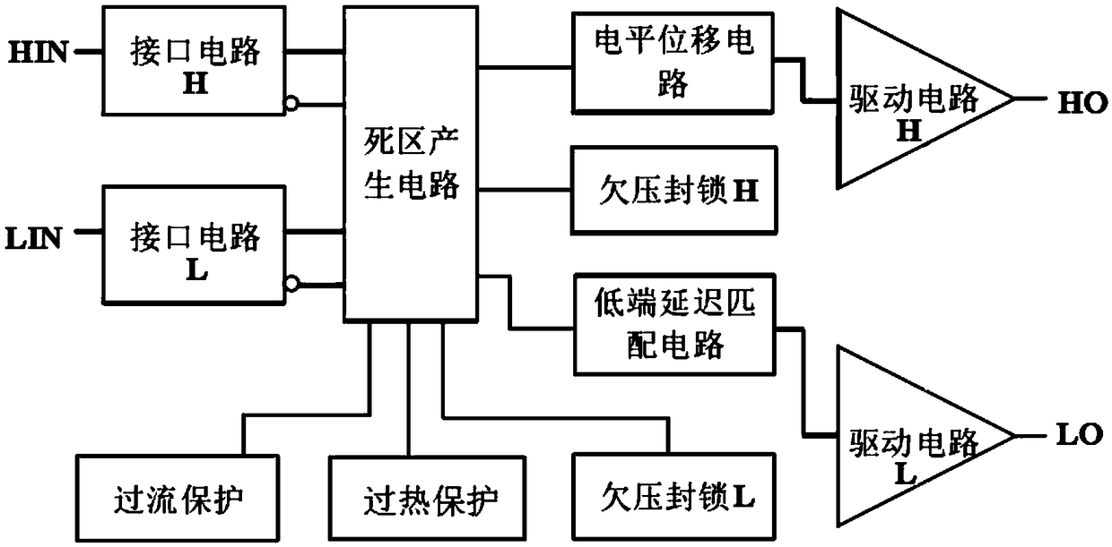
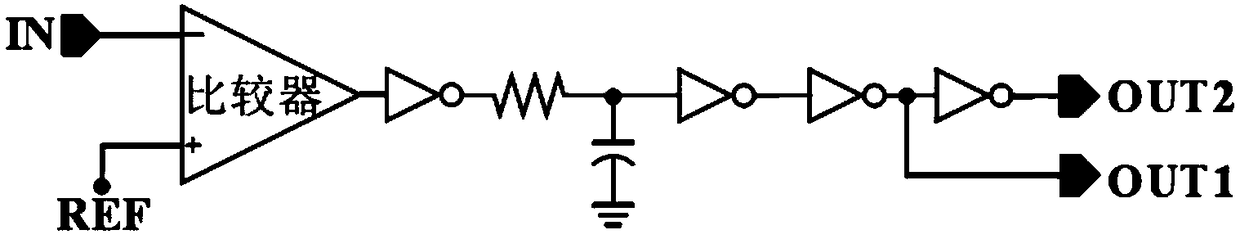
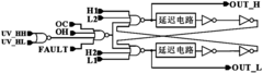
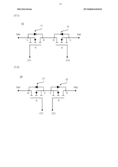
Gate driving circuit with protection function for enhanced GaN power device
PatentActiveCN109495095A
Innovation
- An enhanced GaN power device gate drive circuit with multiple protection functions is designed, including interface circuit, dead zone generation circuit, level shift circuit, low-end delay matching circuit, drive circuit, under-voltage blocking circuit, over-current Protection circuit and overheating protection circuit, through these circuits, they automatically detect overheating, power supply voltage undervoltage or overcurrent, and shut down the drive circuit to protect GaN power devices.
Driving apparatus and driving method for gallium nitride device
PatentWO2024196166A1
Innovation
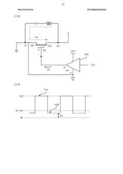
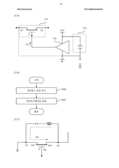
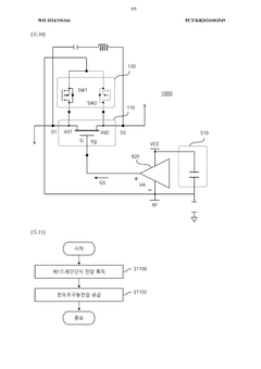
- A gallium nitride (GaN) device driving method using a gate driver with a reference voltage generated from the lower voltage of the GaN device's drain terminals, and a voltage selector with parasitic diodes to minimize power loss and eliminate the need for parasitic diodes in the GaN device, allowing for bidirectional voltage blocking.
Thermal Management Considerations for GaN Gate Drivers
Thermal management is a critical aspect of GaN gate driver design that significantly impacts the overall performance and reliability of GaN power devices. The inherent high-speed switching capability of GaN devices, while beneficial for efficiency, generates substantial thermal stress on gate drivers. These thermal challenges are exacerbated by the compact packaging requirements of modern power electronics systems, creating a complex thermal environment that must be carefully managed.
Gate drivers for GaN devices typically operate at higher frequencies than their silicon counterparts, resulting in increased switching losses and heat generation. This heat must be effectively dissipated to prevent thermal runaway conditions that could lead to catastrophic failure. The thermal resistance path from the gate driver IC to the ambient environment plays a crucial role in determining the maximum operating temperature and, consequently, the reliability of the system.
Several thermal management strategies have emerged to address these challenges. Advanced packaging technologies, such as flip-chip and direct bonding, help minimize thermal resistance between the gate driver and its heat sink. These approaches reduce the thermal path length and improve heat dissipation efficiency, allowing for higher power density designs.
Active cooling solutions, including forced air and liquid cooling systems, are increasingly being employed in high-power GaN applications. These systems provide enhanced thermal performance but must be carefully integrated to avoid introducing electromagnetic interference that could compromise the gate driver's operation. Passive cooling techniques, such as optimized PCB layout with thermal vias and copper planes, remain fundamental to effective thermal management.
Thermal simulation and modeling have become essential tools in the design process. Computational fluid dynamics (CFD) and finite element analysis (FEA) enable designers to predict thermal behavior under various operating conditions, optimizing heat dissipation before physical prototyping. These simulation tools help identify potential hotspots and validate cooling strategies early in the design cycle.
Temperature monitoring and protection circuits are now standard features in advanced GaN gate driver designs. These circuits continuously monitor the operating temperature and can implement protective measures, such as reducing switching frequency or shutting down the system, when thermal limits are approached. Such dynamic thermal management extends the operational lifetime of GaN power systems while maintaining safe operating conditions.
The thermal interface materials (TIMs) between the gate driver and cooling elements represent another critical consideration. Advanced TIMs with high thermal conductivity and reliability under temperature cycling are essential for maintaining consistent thermal performance throughout the system's operational life.
EMI/EMC Compliance for GaN-based Power Systems
Electromagnetic Interference (EMI) and Electromagnetic Compatibility (EMC) compliance represent critical challenges in GaN-based power systems due to the high switching speeds and steep voltage transitions inherent to GaN technology. These characteristics, while beneficial for efficiency, generate significant electromagnetic noise that must be properly managed to meet regulatory standards and ensure reliable operation in various applications.
The fast switching transitions of GaN devices (typically 10-100 V/ns) create high-frequency noise components that can propagate through conducted and radiated paths. This noise generation is directly influenced by gate drive strategies, particularly the isolation methods employed and Miller effect management techniques. Proper isolation between control and power circuits becomes essential not only for safety but also for minimizing common-mode noise paths that contribute to EMI issues.
Traditional EMI/EMC mitigation techniques often prove insufficient for GaN-based systems due to the higher frequency content of the generated noise. Conventional filter designs may require significant modification, with particular attention to parasitic elements that become increasingly influential at higher frequencies. The layout considerations for GaN power systems must account for minimizing loop areas and strategic placement of components to reduce both conducted and radiated emissions.
Protection circuits implemented in gate drive strategies can inadvertently impact EMI/EMC performance. For instance, fast-acting overcurrent protection may introduce additional switching events that generate spurious emissions. Therefore, protection mechanisms must be designed with consideration for their potential EMI contributions, balancing response time with clean switching transitions.
Compliance testing for GaN-based systems typically requires evaluation across broader frequency ranges than traditional silicon-based power electronics. Standards such as CISPR 11, CISPR 22, and FCC Part 15 establish limits for conducted and radiated emissions that GaN systems must meet, often necessitating comprehensive shielding and filtering solutions specifically tailored to the unique characteristics of GaN switching behavior.
Recent research indicates that soft-switching techniques, when implemented through appropriate gate drive strategies, can significantly reduce EMI while maintaining the efficiency benefits of GaN technology. These approaches modify the switching trajectory to reduce dv/dt and di/dt rates at critical points in the switching cycle, thereby attenuating high-frequency noise components without substantially increasing switching losses.
The interplay between gate drive parameters (voltage levels, rise/fall times) and EMI generation presents opportunities for adaptive control strategies that dynamically adjust switching characteristics based on operating conditions, potentially optimizing the balance between performance and electromagnetic compliance.
Unlock deeper insights with Patsnap Eureka Quick Research — get a full tech report to explore trends and direct your research. Try now!
Generate Your Research Report Instantly with AI Agent
Supercharge your innovation with Patsnap Eureka AI Agent Platform!