Roadmap For GaN Power Devices: 8-Inch Wafers, E-Mode Reliability, And Next-Gen Packages
AUG 26, 20259 MIN READ
Generate Your Research Report Instantly with AI Agent
Patsnap Eureka helps you evaluate technical feasibility & market potential.
GaN Power Devices Evolution and Objectives
Gallium Nitride (GaN) power devices have emerged as a revolutionary technology in the power electronics industry over the past two decades. The evolution of GaN technology began in the early 2000s with research focused primarily on RF applications, but quickly expanded into power electronics due to its superior material properties compared to silicon. GaN offers higher breakdown voltage, faster switching speeds, and lower on-resistance, making it ideal for high-frequency, high-power applications.
The technological trajectory of GaN power devices has been marked by several significant milestones. Initially, development centered on lateral GaN-on-Si devices, which offered a cost-effective manufacturing approach by leveraging existing silicon infrastructure. This was followed by advancements in epitaxial growth techniques, enabling higher quality GaN layers with fewer defects and improved performance characteristics.
Recent years have witnessed a shift toward commercial viability, with the introduction of 600V and 650V GaN devices for consumer electronics, industrial power supplies, and automotive applications. The industry is now at a critical juncture, transitioning from early adoption to mainstream implementation, with increasing focus on reliability, manufacturability, and cost reduction.
The current technological objectives for GaN power devices center around three key areas: scaling to 8-inch wafers, enhancing enhancement-mode (E-mode) device reliability, and developing next-generation packaging solutions. The transition to 8-inch wafers represents a crucial step toward cost reduction and manufacturing scalability, potentially decreasing production costs by 20-30% compared to current 6-inch wafer processes.
E-mode reliability improvement addresses one of the most significant barriers to widespread GaN adoption. Current objectives include extending device lifetime under high-temperature, high-voltage conditions, with targets exceeding 10 years of operational life at rated conditions. This involves innovations in gate structure, passivation techniques, and field management strategies.
Next-generation packaging solutions aim to fully exploit GaN's inherent high-frequency capabilities. Traditional packaging technologies often introduce parasitic inductances and capacitances that limit switching performance. Advanced packaging concepts, including chip-scale packaging and integrated multi-chip modules, are being developed to minimize these parasitic effects and enable switching frequencies exceeding 10 MHz.
The overarching goal of these technological objectives is to position GaN power devices as the dominant technology for medium-voltage (100V-900V) power applications, offering superior efficiency, power density, and system-level cost benefits compared to silicon and silicon carbide alternatives. Industry projections suggest that achieving these objectives could expand the GaN power device market from approximately $100 million today to over $1 billion by 2026.
Market Demand Analysis for GaN Power Electronics
The global market for GaN power electronics is experiencing unprecedented growth, driven by the increasing demand for high-efficiency power conversion systems across multiple industries. Current market valuations place the GaN power device sector at approximately 1.1 billion USD in 2023, with projections indicating a compound annual growth rate (CAGR) of 25-30% through 2030, potentially reaching 5.7 billion USD by the end of the decade. This remarkable expansion significantly outpaces the broader semiconductor industry's average growth rate of 4-6%.
The automotive sector represents the largest and fastest-growing market segment for GaN power electronics, particularly with the rapid adoption of electric vehicles (EVs). The need for more efficient onboard chargers, DC-DC converters, and traction inverters is creating substantial demand for GaN solutions that can reduce power losses by 40-50% compared to traditional silicon-based alternatives. Industry forecasts suggest that by 2028, over 35% of new EVs will incorporate GaN power devices in at least one power conversion system.
Consumer electronics constitutes another significant market driver, with manufacturers increasingly adopting GaN technology for fast chargers and power adapters. The smaller form factor and higher efficiency of GaN-based chargers have created a premium segment within the consumer charging market, with adoption rates increasing by approximately 78% year-over-year since 2021. Major smartphone and laptop manufacturers have already transitioned to GaN charging solutions, creating a market expected to exceed 2 billion USD by 2026.
Industrial power systems and renewable energy applications represent emerging high-growth segments for GaN technology. Solar inverters utilizing GaN can achieve efficiency improvements of 2-3 percentage points over silicon alternatives, translating to significant energy savings at scale. The industrial motor drive market is similarly poised for GaN adoption, with the potential to reduce energy consumption by 10-15% in variable frequency drive applications.
Regional analysis reveals that Asia-Pacific currently dominates GaN power device consumption, accounting for approximately 58% of global demand, followed by North America (22%) and Europe (17%). However, North America is experiencing the fastest growth rate at 32% annually, driven by aggressive electrification initiatives and substantial investments in renewable energy infrastructure.
The transition to 8-inch wafers represents a critical inflection point for market expansion, as it promises to reduce manufacturing costs by 25-30% compared to current 6-inch wafer production. This cost reduction is expected to accelerate GaN adoption in price-sensitive applications and open new market segments previously dominated by silicon devices. Industry analysts predict that achieving price parity with silicon alternatives in medium-power applications could expand the addressable market by an additional 3-4 billion USD by 2030.
Current Challenges in 8-Inch GaN Wafer Production
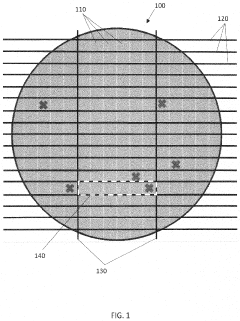
The transition to 8-inch GaN wafer production represents a critical inflection point in the power electronics industry, promising significant cost reductions and manufacturing efficiencies. However, this scaling process faces substantial technical hurdles that have slowed widespread adoption. The most fundamental challenge lies in maintaining crystal quality while increasing wafer diameter, as GaN materials are prone to higher dislocation densities and wafer bow when scaled to larger sizes.
Material uniformity presents another significant obstacle, with 8-inch GaN wafers exhibiting greater thickness variations and compositional inconsistencies compared to their 6-inch counterparts. These non-uniformities directly impact device performance parameters such as breakdown voltage and on-resistance, leading to yield issues in high-volume manufacturing environments.
Thermal management during epitaxial growth becomes increasingly complex with larger wafers. The temperature gradients across 8-inch platforms are more pronounced, resulting in uneven material properties from center to edge. Current MOCVD (Metal Organic Chemical Vapor Deposition) reactor designs require substantial modifications to accommodate these larger substrates while maintaining thermal uniformity throughout the growth process.
Substrate availability represents a persistent bottleneck, with high-quality 8-inch silicon carbide and native GaN substrates remaining prohibitively expensive for mass production. While silicon substrates offer cost advantages, the lattice and thermal expansion coefficient mismatches with GaN epitaxial layers become more problematic at the 8-inch scale, leading to increased wafer warpage and stress-induced defects.
Equipment compatibility issues further complicate the transition, as many existing fabrication tools designed for 6-inch wafers require significant retrofitting or complete replacement to handle 8-inch GaN wafers. This necessitates substantial capital investment from manufacturers, slowing industry-wide adoption despite the long-term economic benefits.
Metrology and inspection capabilities must also evolve to effectively characterize these larger wafers. Current techniques struggle to maintain the necessary resolution and throughput when scaled to 8-inch dimensions, creating challenges in defect detection and process control that are critical for maintaining yield metrics.
The economic considerations cannot be overlooked, as the initial investment required for 8-inch GaN production lines remains substantial. Despite the theoretical cost advantages of larger wafers, the transition period involves significant financial risk that smaller manufacturers find difficult to justify without guaranteed volume commitments from customers.
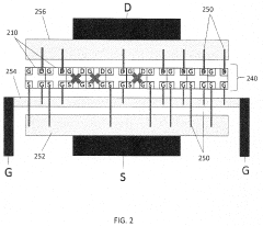
E-Mode GaN Reliability Solutions
01 GaN wafer size advancements for power devices
The evolution of GaN wafer sizes has been significant for power device manufacturing, with transitions from smaller diameters to larger ones (4-inch, 6-inch, 8-inch) enabling more cost-effective production. Larger wafer sizes allow for higher throughput, reduced manufacturing costs per device, and better integration with standard silicon manufacturing infrastructure. These advancements have been crucial for the commercial viability of GaN power devices, particularly for high-voltage and high-frequency applications.- GaN wafer size advancements for power devices: Advancements in gallium nitride (GaN) wafer sizes have significantly impacted power device manufacturing. Larger wafer sizes, evolving from 2-inch to 6-inch and beyond, enable more efficient production and cost reduction. These larger substrates allow for higher yield and better economies of scale in GaN power device fabrication. The transition to larger wafer sizes addresses manufacturing challenges while maintaining crystal quality necessary for high-performance power applications.
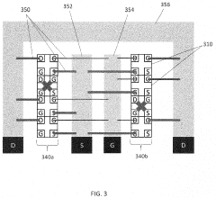
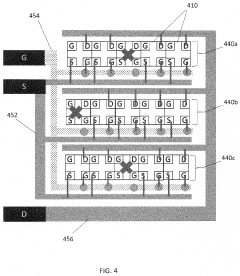
- Reliability enhancement techniques for GaN power devices: Various techniques have been developed to enhance the reliability of GaN power devices. These include improved passivation layers, optimized gate structures, and advanced stress testing methodologies. Thermal management solutions and novel buffer layer designs help mitigate common failure mechanisms such as current collapse and dynamic RON degradation. Reliability testing protocols specific to GaN devices have been established to ensure long-term stability under various operating conditions, including high temperature and high voltage stress scenarios.
- Advanced packaging solutions for GaN power devices: Innovative packaging technologies have been developed specifically for GaN power devices to maximize their performance advantages. These include chip-scale packaging, flip-chip configurations, and embedded die technologies that minimize parasitic inductances and thermal resistance. Advanced interconnect materials and structures enable higher switching frequencies while maintaining thermal stability. Multi-chip module approaches integrate GaN devices with silicon-based control circuits in compact, high-performance packages suitable for demanding applications.
- Thermal management strategies for GaN power devices: Effective thermal management is critical for GaN power device reliability and performance. Advanced cooling solutions include novel die-attach materials with enhanced thermal conductivity, integrated heat spreaders, and optimized package designs that facilitate heat dissipation. Direct substrate cooling techniques and advanced thermal interface materials help maintain lower junction temperatures during high-power operation. Simulation and modeling approaches enable accurate prediction of thermal behavior under various operating conditions to optimize device design and packaging.
- Integration and manufacturing processes for GaN power devices: Specialized manufacturing processes have been developed for GaN power device integration. These include epitaxial growth optimization on various substrates, selective area growth techniques, and advanced lithography processes for high-resolution features. Novel approaches for GaN-on-silicon integration enable cost-effective production while addressing challenges related to lattice mismatch and thermal expansion differences. Process innovations in metallization, dielectric deposition, and etching contribute to improved device performance and manufacturing yield.
02 Reliability enhancement techniques for GaN power devices
Various techniques have been developed to enhance the reliability of GaN power devices, including improved passivation layers, optimized gate structures, and stress testing methodologies. These approaches address common failure mechanisms such as current collapse, dynamic RON degradation, and threshold voltage instability. Advanced reliability testing protocols have been established to evaluate device performance under various operational conditions, including high temperature, high voltage, and switching stress tests, ensuring long-term stability and performance.Expand Specific Solutions03 Advanced packaging solutions for GaN power devices
Innovative packaging technologies have been developed specifically for GaN power devices to optimize thermal management, reduce parasitic inductance, and enhance overall performance. These include flip-chip configurations, embedded die technologies, and direct copper bonding. Advanced packaging solutions address the unique challenges of GaN devices, such as high switching frequencies and thermal dissipation requirements, while enabling compact form factors for space-constrained applications.Expand Specific Solutions04 Integration of GaN with silicon substrates and other materials
The integration of GaN with silicon substrates and other materials has been a key focus area for improving cost-effectiveness and performance of power devices. Various epitaxial growth techniques and buffer layer designs have been developed to manage the lattice mismatch and thermal expansion differences between GaN and substrate materials. This integration enables the fabrication of GaN-on-Si power devices that combine the superior electrical properties of GaN with the cost advantages and established manufacturing infrastructure of silicon technology.Expand Specific Solutions05 Testing and qualification methodologies for GaN power devices
Specialized testing and qualification methodologies have been developed for GaN power devices to ensure performance, reliability, and safety across various applications. These include accelerated life testing, dynamic characterization techniques, and standardized qualification procedures. Advanced testing approaches address the unique characteristics of GaN devices, such as high-frequency operation and different failure mechanisms compared to silicon devices, providing manufacturers and end-users with confidence in long-term device performance under real-world conditions.Expand Specific Solutions
Leading Manufacturers and Competitive Landscape
The GaN power devices market is transitioning from early adoption to growth phase, with an expanding market projected to reach several billion dollars by 2026. The industry is advancing toward technological maturity with key developments in 8-inch wafer production, enhanced-mode device reliability, and advanced packaging solutions. Companies like Cambridge GaN Devices, GaN Systems, and Texas Instruments are leading commercial innovation, while academic institutions including MIT, Arizona State University, and Xidian University contribute significant research. UMC and Siltronic are advancing manufacturing capabilities for larger wafers. The competitive landscape features established semiconductor players and specialized GaN startups collaborating with automotive and industrial partners to overcome reliability challenges and drive adoption in high-power applications.
Cambridge GaN Devices Ltd.
Technical Solution: Cambridge GaN Devices (CGD) has developed a proprietary ICeGaN™ (Integrated Circuit Enhancement-mode GaN) technology platform specifically addressing the E-mode reliability challenges in GaN power devices. Their approach integrates gate protection and drive circuitry directly into the GaN chip, creating a truly "normally-off" device with significantly improved gate robustness. CGD has successfully implemented their technology on 8-inch GaN-on-Si wafers, collaborating with major foundries to ensure manufacturing scalability. Their devices feature a gate threshold voltage of +3V (compared to traditional E-mode GaN at +1.5V), providing enhanced noise immunity and safer operation. The company's reliability testing demonstrates gate robustness exceeding 10 million switching cycles without degradation and stable operation after 1000+ hours of HTGB testing at 150°C. For packaging, CGD employs advanced clip-bonding techniques that reduce parasitic inductance by approximately 60% compared to wire-bonded alternatives.
Strengths: Superior gate reliability with integrated protection; silicon-like driving characteristics requiring no special gate drivers; compatible with standard manufacturing processes. Weaknesses: Relatively new market entrant with limited production history; smaller product portfolio compared to established competitors; higher cost structure until production volumes increase.
Huawei Technologies Co., Ltd.
Technical Solution: Huawei has developed an advanced GaN power device roadmap focusing on high-frequency, high-efficiency power conversion for telecommunications and data center applications. Their GaN technology utilizes 8-inch GaN-on-Si wafers manufactured through strategic foundry partnerships, enabling cost-effective scaling. Huawei's E-mode GaN devices incorporate a unique "hybrid drain" structure that optimizes the trade-off between on-resistance and breakdown voltage, achieving RDS(on) values below 25mΩ for 650V-rated devices. For reliability enhancement, they've implemented a proprietary passivation layer technology that significantly reduces current collapse under switching conditions and improves threshold voltage stability during long-term operation. Their packaging innovation includes a "cooling-enhanced package" (CEP) design that reduces thermal resistance by approximately 30% compared to standard packages, enabling higher power density. Huawei has also pioneered integrated GaN power modules that combine multiple GaN HEMTs with gate drivers and protection circuits in a single package, reducing system complexity.
Strengths: Vertical integration from device design to system implementation; extensive real-world deployment experience in telecom infrastructure; advanced thermal management solutions. Weaknesses: Limited commercial availability outside their own systems; potential geopolitical challenges affecting global market access; higher focus on specific application segments rather than broad market coverage.
Next-Generation Packaging Innovations for GaN
Defect-Tolerant Layout and Packaging for GaN Power Devices
PatentActiveUS20190378822A1
Innovation
- The solution involves dividing GaN power switching device dies into smaller sub-devices, identifying and selectively connecting only functional sub-devices in a parallel arrangement during packaging, using techniques like wire bonding or metal bumping, to exclude defective sub-devices and increase yield, particularly suitable for lateral power devices.
Electronic device with enhancement mode gallium nitride transistor, and method of making same
PatentWO2022093731A1
Innovation
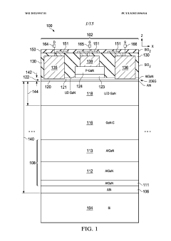
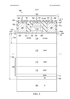
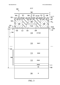
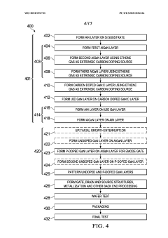
- The electronic device incorporates a buffer structure and hetero-epitaxy structure with a gallium nitride interlayer and a p-doped gallium nitride layer, where the p-doped layer has a peak p-type dopant concentration significantly higher than the interlayer, and an undoped or low-doped gallium nitride interlayer is used to mitigate dopant diffusion, forming an enhancement mode transistor with a gate over the p-doped layer and drain/source in the hetero-epitaxy structure.
Thermal Management Strategies for GaN Devices
Thermal management represents a critical challenge in the advancement of GaN power devices, particularly as the industry moves toward 8-inch wafers and enhanced power densities. The superior electrical properties of GaN, including high electron mobility and breakdown voltage, enable devices to operate at higher frequencies and power levels than silicon counterparts, but simultaneously generate significant thermal loads that must be efficiently dissipated.
Current thermal management approaches for GaN devices primarily focus on substrate selection and package design optimization. Silicon carbide (SiC) substrates offer thermal conductivity approximately three times higher than silicon, making them increasingly preferred for high-power applications despite their higher cost. Advanced cooling techniques including direct liquid cooling, two-phase cooling systems, and microchannel coolers are being implemented to address the thermal challenges in next-generation packages.
The thermal resistance junction-to-case (RθJC) remains a key performance indicator for GaN devices, with industry leaders working to reduce this parameter below 0.5°C/W for high-power applications. This improvement is essential for enabling the full potential of 8-inch wafer production and ensuring device reliability under extreme operating conditions.
Emerging thermal interface materials (TIMs) with enhanced thermal conductivity are being developed specifically for GaN applications. These include metal-based TIMs, carbon nanotube arrays, and graphene-enhanced composites that can reduce thermal boundary resistance between the device and heat sink by up to 40% compared to conventional materials.
Simulation and modeling tools have become increasingly sophisticated in predicting thermal behavior in GaN devices. Multi-physics simulation platforms now integrate electrical, thermal, and mechanical analyses to provide comprehensive design insights before physical prototyping. These tools are particularly valuable for optimizing next-generation packages that must balance thermal performance with electrical parasitics and mechanical reliability.
Active cooling solutions, including thermoelectric coolers and microfluidic systems integrated directly into device packages, represent the cutting edge of thermal management for high-performance GaN applications. These approaches can maintain junction temperatures below critical thresholds even under extreme operating conditions, though they add complexity and cost to the overall system.
The roadmap for thermal management in GaN power devices must address not only performance but also manufacturing scalability as the industry transitions to 8-inch wafers. Thermal solutions must be compatible with high-volume production techniques while maintaining the reliability improvements necessary for widespread commercial adoption.
Cost-Performance Analysis of GaN vs Silicon Technologies
The economic comparison between Gallium Nitride (GaN) and traditional Silicon (Si) technologies reveals a complex landscape of cost-performance trade-offs that are evolving rapidly. Currently, GaN power devices command a premium price point compared to their silicon counterparts, with manufacturing costs approximately 2-3 times higher. This cost differential stems primarily from lower production volumes, specialized fabrication requirements, and the higher material costs associated with GaN substrates.
However, the performance advantages of GaN technology offer compelling value propositions that increasingly justify the higher initial investment. GaN devices demonstrate superior power density (approximately 3-4 times higher than silicon), enabling smaller form factors and reduced system-level costs. The higher switching frequencies achievable with GaN (up to 10 times that of silicon devices) translate to smaller passive components, further reducing overall system size and cost.
The transition to 8-inch wafer production represents a critical inflection point in the cost trajectory of GaN technology. Industry analysis indicates that this scale-up could reduce manufacturing costs by 25-30% compared to current 6-inch wafer processes. Major manufacturers are projecting that with increased production volumes and improved yields, the cost gap between GaN and silicon could narrow to 1.3-1.5 times by 2025.
From a total cost of ownership perspective, GaN-based power systems demonstrate advantages in energy efficiency, with typical improvements of 10-20% in power conversion efficiency compared to silicon solutions. This efficiency translates directly to operational cost savings, particularly in high-power applications where energy consumption represents a significant expense over the device lifetime.
The reliability improvements in enhancement-mode (E-mode) GaN devices are further strengthening the economic case. While early GaN implementations suffered from reliability concerns that increased lifetime costs, recent advancements have extended operational lifetimes to levels competitive with silicon technologies, reducing replacement and maintenance expenses.
Next-generation packaging innovations are simultaneously driving down implementation costs while enhancing performance. Advanced packaging techniques specific to GaN's unique characteristics are enabling better thermal management and higher power density, creating a virtuous cycle of performance improvement and cost reduction at the system level.
Market forecasts suggest that as production volumes increase and manufacturing processes mature, GaN device costs will continue to decline at approximately 15% annually, potentially reaching price parity with silicon in specific application segments by 2028-2030. This cost trajectory, combined with the inherent performance advantages, positions GaN technology to achieve increasingly favorable cost-performance ratios across expanding application domains.
Unlock deeper insights with Patsnap Eureka Quick Research — get a full tech report to explore trends and direct your research. Try now!
Generate Your Research Report Instantly with AI Agent
Supercharge your innovation with Patsnap Eureka AI Agent Platform!