GaN Power Devices Versus Superjunction MOSFETs In 650V Applications
AUG 26, 20259 MIN READ
Generate Your Research Report Instantly with AI Agent
Patsnap Eureka helps you evaluate technical feasibility & market potential.
GaN vs SJ MOSFET Technology Evolution and Objectives
Power electronics has witnessed a significant evolution over the past decades, with silicon-based devices dominating the market for many years. However, as power systems demand higher efficiency, faster switching speeds, and smaller form factors, traditional silicon MOSFETs have reached their theoretical limits. This technological plateau has driven the emergence of wide bandgap (WBG) semiconductors, particularly Gallium Nitride (GaN), as potential alternatives to silicon-based Superjunction (SJ) MOSFETs in the 650V application space.
The development of SJ MOSFETs began in the late 1990s as an enhancement to conventional silicon MOSFETs, utilizing a unique vertical charge-balanced structure to overcome the silicon material limitations. This innovation allowed SJ MOSFETs to achieve significantly lower on-resistance per unit area compared to conventional MOSFETs, making them the industry standard for high-voltage applications between 500V and 900V for over two decades.
GaN technology, meanwhile, has been evolving from its initial applications in optoelectronics and RF amplifiers toward power electronics. The fundamental material properties of GaN, including its wider bandgap (3.4 eV compared to silicon's 1.1 eV), higher critical electric field, and superior electron mobility, theoretically position it as a superior alternative to silicon in high-voltage, high-frequency applications.
The technological trajectory for both technologies has been driven by several key objectives: reducing switching losses, minimizing conduction losses, improving thermal performance, enhancing reliability, and decreasing overall system costs. For 650V applications specifically, these objectives translate into power devices that can operate efficiently at higher frequencies while maintaining robust performance under demanding conditions.
Recent advancements in GaN epitaxial growth techniques, particularly the development of GaN-on-Si technology, have significantly reduced manufacturing costs, making GaN power devices increasingly competitive with SJ MOSFETs. Simultaneously, SJ MOSFET technology continues to evolve through finer cell pitches, improved trench structures, and enhanced packaging technologies to maintain its market position.
The convergence point of these two technologies in the 650V space represents a critical juncture in power electronics evolution. This voltage rating is particularly significant as it serves numerous applications including server power supplies, telecom rectifiers, industrial motor drives, and increasingly, electric vehicle onboard chargers and solar inverters.
The technological objectives for both GaN and SJ MOSFETs in this competitive landscape focus on achieving the optimal balance between performance parameters, reliability metrics, and cost considerations. As both technologies continue to mature, their respective development roadmaps indicate a fascinating technological race that will significantly influence the future direction of power electronics design and implementation.
Market Demand Analysis for 650V Power Applications
The 650V power device market is experiencing robust growth driven by increasing demand across multiple sectors including electric vehicles (EVs), renewable energy systems, industrial automation, and data centers. The global market for 650V power applications reached approximately $3.2 billion in 2022 and is projected to grow at a CAGR of 11.8% through 2028, reflecting the critical role these devices play in modern power conversion systems.
Electric vehicle adoption represents the most significant growth driver for 650V power devices. With global EV sales surpassing 10 million units in 2022, the demand for efficient power conversion in onboard chargers, DC-DC converters, and traction inverters has intensified. The automotive sector now accounts for nearly 35% of the total 650V power device market, with this share expected to increase as EV penetration accelerates globally.
Renewable energy applications constitute another major demand segment. Solar inverters and wind power converters require high-efficiency power devices to minimize conversion losses. The global solar PV capacity additions reached 239 GW in 2022, creating substantial demand for advanced 650V power solutions that can improve system efficiency and reduce cooling requirements.
Data center power infrastructure represents a rapidly expanding application area, driven by cloud computing and AI workloads. The need for more efficient power supplies and server power delivery systems has created a premium market segment where performance advantages of newer technologies like GaN can command price premiums despite higher initial costs.
Industrial automation and motor drives form a stable but growing segment for 650V devices. Variable frequency drives and industrial power supplies increasingly demand higher efficiency and power density, creating opportunities for both established Superjunction MOSFET technologies and emerging GaN solutions.
Consumer electronics, particularly high-end power supplies and fast chargers, have become an important proving ground for GaN technology at the 650V node. This segment has demonstrated willingness to adopt new technologies when performance advantages are clear, with GaN-based fast chargers gaining significant market share since 2020.
Regional analysis shows Asia-Pacific dominating the market with approximately 65% share, driven by manufacturing concentration in China, Japan, and South Korea. North America and Europe follow with 18% and 14% respectively, with particular strength in high-performance applications where efficiency premiums justify higher component costs.
The market exhibits price sensitivity varying by application segment. While consumer and some industrial applications remain highly cost-conscious, automotive and data center segments demonstrate greater willingness to pay premiums for performance advantages, creating entry points for newer technologies like GaN despite their current cost disadvantages compared to mature Superjunction MOSFET solutions.
Technical Status and Challenges in Wide Bandgap Semiconductors
Wide bandgap (WBG) semiconductors, particularly Gallium Nitride (GaN) and Silicon Carbide (SiC), represent a significant advancement in power electronics technology. The current technical landscape shows GaN power devices gaining substantial traction in 650V applications, challenging the established Superjunction MOSFET technology. Global research institutions and semiconductor manufacturers have achieved remarkable progress in GaN device fabrication, with enhanced electron mobility, reduced on-resistance, and improved thermal performance.
The fundamental advantage of GaN lies in its superior material properties - a bandgap of 3.4 eV compared to silicon's 1.1 eV, enabling higher breakdown voltage capabilities. Current GaN devices demonstrate specific on-resistance approximately ten times lower than silicon-based alternatives at equivalent voltage ratings, translating to significantly reduced conduction losses in power conversion systems.
Despite these advancements, several technical challenges persist in GaN technology implementation. The heteroepitaxial growth of GaN on silicon substrates introduces defect densities that can compromise long-term reliability. Current manufacturing processes face yield challenges when scaling to larger wafer sizes, impacting production economics. Additionally, dynamic RDS(on) degradation under high-voltage switching conditions remains a concern for certain GaN device architectures.
Superjunction MOSFETs, the incumbent technology in 650V applications, have undergone continuous refinement with the latest generations achieving impressive performance metrics. These devices utilize charge-balanced structures to overcome the silicon theoretical limit, but are approaching physical boundaries for further improvement. Their mature ecosystem and established reliability data provide a competitive advantage against emerging GaN solutions.
Geographically, GaN power device development shows distinct regional characteristics. North American companies lead in innovative device architectures and IP development, while Asian manufacturers, particularly in Japan and China, excel in high-volume production capabilities. European research institutions contribute significantly to reliability studies and application-specific optimizations.
The technical constraints limiting wider GaN adoption include gate drive complexity, parasitic inductance sensitivity, and thermal management challenges. Current GaN devices typically require careful consideration of switching speed control to manage electromagnetic interference, often necessitating more sophisticated gate driver designs than traditional silicon devices.
Recent technical breakthroughs include the development of p-GaN gate structures that enable enhancement-mode operation, simplifying driver requirements. Advanced packaging technologies incorporating embedded die techniques have also emerged, addressing thermal and parasitic inductance challenges simultaneously. These innovations are gradually removing barriers to GaN adoption in mainstream power conversion applications.
Current Solutions for 650V Power Switching Applications
01 Switching performance comparison between GaN and SJ MOSFETs
GaN power devices generally demonstrate superior switching performance compared to Superjunction MOSFETs due to their lower gate charge and output capacitance. This results in faster switching speeds, reduced switching losses, and higher efficiency in high-frequency applications. The inherent material properties of GaN, including higher electron mobility and critical electric field strength, enable these performance advantages in power conversion systems.- Switching performance comparison between GaN and SJ MOSFETs: GaN power devices generally demonstrate superior switching performance compared to Superjunction MOSFETs due to their lower gate charge and output capacitance. This results in faster switching speeds, reduced switching losses, and higher efficiency in power conversion applications. The higher electron mobility in GaN allows for faster transition between on and off states, making them particularly advantageous in high-frequency applications where Superjunction MOSFETs face limitations due to their inherent silicon material properties.
- Thermal performance and reliability comparison: Thermal management differs significantly between GaN devices and Superjunction MOSFETs. While SJ MOSFETs typically have better thermal conductivity due to their silicon substrate, GaN devices often operate at higher junction temperatures. The reliability aspects also vary, with GaN devices showing advantages in terms of robustness against voltage spikes but facing challenges related to dynamic on-resistance. Long-term reliability testing shows different degradation mechanisms between the two technologies, impacting their suitability for various applications.
- On-resistance and conduction loss comparison: GaN power devices offer significantly lower specific on-resistance compared to Superjunction MOSFETs at the same voltage rating, resulting in reduced conduction losses. This advantage stems from GaN's wider bandgap and higher critical electric field strength, allowing for thinner drift regions while maintaining high breakdown voltage. However, the on-resistance of GaN devices tends to increase more with temperature compared to SJ MOSFETs, which can affect performance in high-temperature applications. The figure of merit (Ron × Area) is substantially better for GaN devices, enabling smaller die sizes for the same resistance.
- Integration and packaging technologies: Integration and packaging approaches differ significantly between GaN devices and Superjunction MOSFETs. GaN devices often utilize innovative packaging solutions to minimize parasitic inductances and maximize their inherent high-speed capabilities. These include chip-scale packaging and integrated gate drivers. Superjunction MOSFETs typically use more conventional packaging but benefit from mature manufacturing processes. The co-packaging of GaN with control circuits presents unique challenges compared to silicon-based SJ MOSFETs, affecting overall system performance and cost considerations.
- Application-specific performance trade-offs: The choice between GaN power devices and Superjunction MOSFETs depends heavily on application requirements. GaN devices excel in high-frequency applications (>100kHz) such as compact power adapters, wireless charging, and high-density power supplies due to their superior switching performance. Superjunction MOSFETs remain competitive in high-power applications where thermal management is critical, and in cost-sensitive markets where their mature manufacturing ecosystem provides economic advantages. The breakdown voltage characteristics and reverse recovery behavior also influence their suitability for specific circuit topologies.
02 Thermal performance and reliability comparison
Thermal management differs significantly between GaN devices and Superjunction MOSFETs. While SJ MOSFETs typically have better thermal conductivity and established reliability, GaN devices operate efficiently at higher temperatures but face challenges in heat dissipation due to packaging limitations. Long-term reliability testing shows that properly designed GaN devices can achieve comparable or better lifetime performance in certain applications despite their different failure mechanisms.Expand Specific Solutions03 On-resistance and conduction loss comparison
GaN power devices offer significantly lower specific on-resistance compared to Superjunction MOSFETs at equivalent voltage ratings, resulting in reduced conduction losses. This advantage becomes more pronounced at higher blocking voltages, where GaN's superior material properties allow for thinner drift regions. The lateral structure of GaN HEMTs contributes to this performance advantage, though Superjunction MOSFETs maintain competitive performance in certain voltage ranges through their charge-balanced structure.Expand Specific Solutions04 Application-specific performance trade-offs
The choice between GaN devices and Superjunction MOSFETs depends heavily on application requirements. GaN excels in high-frequency, high-efficiency applications like compact power adapters and wireless charging, while Superjunction MOSFETs remain competitive in high-power applications requiring robust short-circuit capability and avalanche ruggedness. Cost considerations, driver compatibility, and system-level integration also influence the selection between these technologies for specific power conversion designs.Expand Specific Solutions05 Integration and packaging innovations
Advanced packaging and integration techniques are being developed to maximize the performance benefits of both GaN and Superjunction MOSFET technologies. For GaN, lateral device structures enable monolithic integration of multiple components and gate drivers, reducing parasitic inductances. Meanwhile, Superjunction MOSFETs benefit from established packaging technologies with excellent thermal performance. Novel hybrid approaches combining both technologies in complementary configurations are emerging to leverage the strengths of each in next-generation power conversion systems.Expand Specific Solutions
Key Manufacturers and Competitive Landscape
The GaN power devices versus Superjunction MOSFETs market in 650V applications is currently in a growth phase, with the global power semiconductor market expanding rapidly. Major players including Texas Instruments, Infineon Technologies, GaN Systems, and Power Integrations are driving innovation in this competitive landscape. The technology is approaching maturity, with GaN devices increasingly challenging traditional silicon-based MOSFETs due to superior switching performance and efficiency. Companies like Toshiba, Fuji Electric, and NXP are investing heavily in both technologies, while newer entrants such as Tagoretech and Epinovatech are focusing on specialized GaN solutions. Academic institutions including Arizona State University and Xidian University are contributing significant research to advance these technologies, particularly in thermal management and reliability improvements.
Texas Instruments Incorporated
Technical Solution: Texas Instruments has developed a comprehensive GaN power portfolio targeting 650V applications with their LMG series of GaN power stages. Their approach integrates GaN FETs with optimized gate drivers and protection features in a single package, addressing the complex driving requirements of GaN technology[1]. TI's GaN implementation utilizes a cascode configuration that pairs a normally-off silicon MOSFET with a normally-on GaN HEMT, allowing the use of standard gate drive voltages while leveraging GaN's superior switching performance[2]. Their devices feature integrated current sensing, temperature monitoring, and fault protection circuitry. TI's comparative testing demonstrates that their 650V GaN solutions achieve up to 80% reduction in switching losses compared to superjunction MOSFETs at equivalent current ratings, enabling power supply designs with efficiencies exceeding 98% and power densities up to 3x higher than silicon-based alternatives[3]. TI has also developed specialized controllers and digital power ICs specifically optimized for driving GaN power stages in various topologies.
Strengths: Highly integrated solution simplifying GaN implementation; comprehensive protection features enhancing system reliability; extensive design support ecosystem including reference designs and simulation tools. Weaknesses: Cascode configuration introduces additional parasitic elements that can partially offset GaN's inherent performance advantages; limited current handling capability compared to larger discrete devices; higher solution cost compared to discrete implementations.
Infineon Technologies Americas Corp.
Technical Solution: Infineon has developed both advanced superjunction MOSFET technology (CoolMOS™) and GaN power devices (CoolGaN™) for 650V applications. Their CoolMOS™ technology features an innovative vertical charge compensation structure that significantly reduces on-resistance while maintaining high blocking voltage capability[1]. For their GaN portfolio, Infineon employs a unique enhancement-mode (e-mode) GaN-on-Silicon technology with their proprietary hybrid-drain embedded gate injection transistor (HD-GIT) structure that combines normally-off operation with robust performance[2]. This architecture provides self-clamping capability during switching transients and superior short-circuit robustness compared to other GaN implementations. Infineon's comparative analysis shows their 650V CoolGaN™ devices achieve up to 50% reduction in switching losses compared to superjunction MOSFETs, while their latest generation CoolMOS™ devices offer the industry's lowest RDS(on) per unit area for silicon-based solutions[3].
Strengths: Comprehensive portfolio offering both advanced superjunction and GaN solutions; strong reliability engineering with extensive qualification testing; established manufacturing infrastructure ensuring supply stability. Weaknesses: Their GaN technology requires specific driving considerations that may complicate implementation; price premium for GaN solutions compared to silicon alternatives; thermal management challenges in high-power density applications.
Critical Patents and Innovations in GaN and SJ MOSFET Technologies
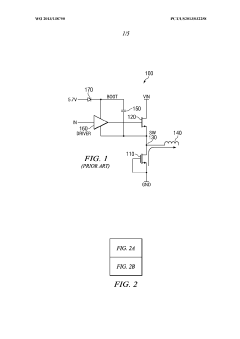
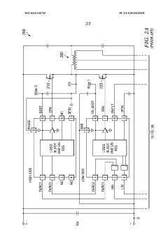
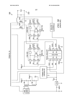
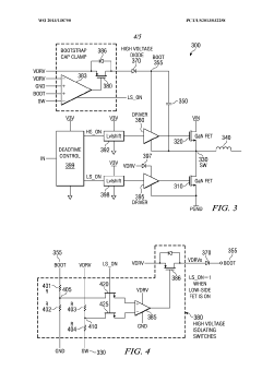
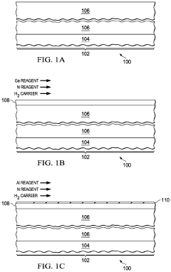
SYSTEM AND APPARATUS FOR DRIVER CIRCUIT FOR PROTECTION OF GATES OF GaN FETS
PatentWO2013138750A1
Innovation
- A bootstrap capacitor clamp (BCC) controller is introduced, comprising a comparator and a field effect transistor, which compares input voltage, ground, and source voltage signals to maintain a safe voltage relationship across the GaN FET's gate, preventing overcharging and ensuring reliable operation by controlling the gate output signal.
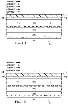
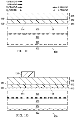
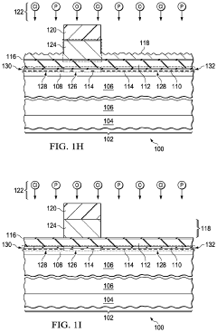
Normally-on gallium nitride based transistor with p-type gate
PatentActiveUS11978790B2
Innovation
- A gallium nitride based low threshold depletion mode transistor with a channel layer of III-N semiconductor material, a barrier layer of aluminum and nitrogen, and a p-type gate of gallium and nitrogen, without a dielectric layer between the gate and the barrier layer, is developed, achieving a threshold potential between −10 volts and −0.1 volts.
Thermal Management and Reliability Considerations
Thermal management represents a critical factor in the performance and reliability of power semiconductor devices, particularly when comparing GaN power devices with Superjunction MOSFETs in 650V applications. GaN devices exhibit fundamentally different thermal characteristics due to their material properties and device structures. While GaN has a higher thermal conductivity (1.3 W/cm·K) than silicon (1.5 W/cm·K), the thin GaN layers grown on substrates like silicon or silicon carbide create thermal bottlenecks that must be addressed in practical applications.
The junction-to-case thermal resistance (Rth,jc) of GaN devices typically ranges from 0.5 to 2.0°C/W, which is comparable to Superjunction MOSFETs. However, GaN devices operate at higher power densities, generating more localized heat that requires sophisticated thermal management solutions. Advanced packaging technologies such as direct bonded copper (DBC) substrates and embedded heat spreaders have been developed specifically to address these thermal challenges in GaN implementations.
Reliability considerations differ significantly between these technologies. Superjunction MOSFETs benefit from decades of silicon device reliability data and established qualification procedures. Their failure mechanisms are well understood, with typical lifetime expectations exceeding 15 years under rated conditions. In contrast, GaN power devices represent a relatively newer technology with evolving reliability standards. Early GaN devices faced challenges related to dynamic Ron (increase in on-resistance during switching), threshold voltage instability, and gate leakage.
Recent advancements in GaN technology have addressed many of these reliability concerns. Current-generation GaN devices undergo rigorous qualification testing including high-temperature reverse bias (HTRB), high-temperature gate bias (HTGB), and temperature humidity bias (THB) tests. Field data indicates that properly designed GaN devices can achieve failure rates below 10 FIT (failures in time, per billion device-hours), approaching the reliability levels of mature silicon technologies.
Temperature cycling capability represents another important distinction. Superjunction MOSFETs typically withstand 1,000+ temperature cycles between -55°C and 150°C, while GaN devices have demonstrated improved cycling capability, now reaching 500-1,000 cycles in recent generations. This improvement stems from optimized die-attach materials and interconnect designs that accommodate the different coefficients of thermal expansion between GaN and package materials.
System-level thermal design must account for these differences. GaN-based power systems often incorporate advanced cooling techniques such as double-sided cooling, phase-change materials, and microfluidic cooling channels to manage the higher power densities. Additionally, thermal simulation tools have evolved to accurately model GaN devices' unique thermal profiles, enabling more precise thermal management strategies in complex power conversion systems.
Cost-Performance Analysis and Manufacturing Scalability
The cost-performance ratio remains a critical factor in the adoption of any new power semiconductor technology. GaN power devices currently command a premium price compared to Superjunction MOSFETs in the 650V application space, with typical cost differentials ranging from 1.5x to 3x depending on current ratings and packaging options. This price gap stems primarily from lower manufacturing volumes and relatively immature production processes for GaN technology.
Performance metrics, however, reveal significant advantages for GaN devices that may justify the higher initial investment. GaN solutions demonstrate 30-40% lower switching losses and enable 3-5x higher switching frequencies compared to Superjunction MOSFETs. These characteristics translate to smaller passive components, reduced cooling requirements, and ultimately more compact power conversion systems with higher power densities.
When evaluating total system costs rather than just component costs, GaN-based designs often achieve 10-15% overall cost savings through reduced heatsink requirements, smaller magnetics, and simplified thermal management. The higher efficiency also contributes to operational cost savings over the product lifetime, particularly in applications with continuous operation profiles.
Manufacturing scalability presents both challenges and opportunities for GaN technology adoption. Current GaN production primarily utilizes 6-inch wafers, while silicon-based Superjunction MOSFET manufacturing has advanced to 12-inch wafers, creating inherent cost disadvantages for GaN. The transition to larger wafer sizes represents a critical inflection point for GaN cost reduction, with several manufacturers announcing roadmaps toward 8-inch GaN-on-Si production by 2024-2025.
Yield rates for GaN devices have improved substantially, from below 70% five years ago to 85-90% today, though still trailing the mature Superjunction MOSFET yields of 95%+. Industry analysts project that continued manufacturing optimization will drive GaN device costs down by approximately 10-15% annually over the next three years, gradually narrowing the price gap with silicon-based alternatives.
Supply chain considerations also impact the cost-performance equation. Superjunction MOSFETs benefit from a diverse, well-established supplier ecosystem, while GaN devices currently face more limited sourcing options. This supply constraint introduces potential risks for high-volume applications but is expected to improve as more semiconductor manufacturers expand their GaN product portfolios.
Foreign trade policies and regional manufacturing incentives are increasingly influencing the cost structures for both technologies, with several countries implementing programs to boost domestic production of wide-bandgap semiconductors, potentially accelerating the cost reduction curve for GaN technology.
Unlock deeper insights with Patsnap Eureka Quick Research — get a full tech report to explore trends and direct your research. Try now!
Generate Your Research Report Instantly with AI Agent
Supercharge your innovation with Patsnap Eureka AI Agent Platform!