How GaN Power Devices Enable PFC + LLC At Megahertz Frequencies
AUG 26, 202510 MIN READ
Generate Your Research Report Instantly with AI Agent
Patsnap Eureka helps you evaluate technical feasibility & market potential.
GaN Power Devices Evolution and Objectives
Gallium Nitride (GaN) power devices have emerged as revolutionary components in power electronics, marking a significant departure from traditional silicon-based technologies. The evolution of GaN power devices began in the early 2000s, primarily driven by the need for higher efficiency, faster switching speeds, and smaller form factors in power conversion systems. Initially developed for military and aerospace applications, GaN technology has gradually transitioned into commercial and industrial sectors over the past decade.
The fundamental advantage of GaN lies in its wide bandgap semiconductor properties, which enable higher breakdown voltages, lower on-resistance, and significantly reduced switching losses compared to silicon counterparts. These characteristics have positioned GaN as an ideal candidate for high-frequency power conversion applications, particularly in Power Factor Correction (PFC) and LLC resonant converters operating at megahertz frequencies.
The technological trajectory of GaN power devices has been marked by continuous improvements in device structure, packaging, and manufacturing processes. Early lateral GaN devices have evolved into more sophisticated structures with enhanced thermal management capabilities and reduced parasitic elements. Concurrently, advancements in packaging technologies have addressed challenges related to thermal dissipation and electromagnetic interference, further expanding the application scope of GaN devices.
Recent years have witnessed a significant reduction in the cost of GaN devices, primarily attributed to improved manufacturing yields and economies of scale. This cost reduction has accelerated the adoption of GaN technology across various power electronics applications, including consumer electronics, automotive systems, and renewable energy converters.
The primary objective of GaN power devices in PFC and LLC applications is to enable operation at megahertz frequencies while maintaining high efficiency and reliability. This goal addresses the growing demand for smaller, lighter, and more efficient power conversion systems in various industries. By operating at megahertz frequencies, GaN-based PFC and LLC converters can significantly reduce the size of passive components, leading to more compact and cost-effective power supply designs.
Another critical objective is to overcome the limitations of silicon-based devices in high-frequency applications, particularly those related to switching losses and thermal management. GaN technology aims to provide a viable solution for next-generation power electronics that require higher power density, improved efficiency, and enhanced reliability under demanding operating conditions.
Looking forward, the evolution of GaN power devices is expected to continue with further improvements in device performance, reliability, and cost-effectiveness. The technology roadmap includes the development of higher voltage ratings, enhanced integration capabilities, and more sophisticated control strategies to fully leverage the potential of GaN in megahertz-frequency power conversion applications.
Market Demand Analysis for High-Frequency Power Conversion
The global power electronics market is experiencing unprecedented growth, driven by the increasing demand for high-frequency power conversion solutions across multiple industries. This market is projected to reach $25 billion by 2026, with a compound annual growth rate of 4.7%. The transition toward megahertz frequency operation in power conversion systems represents a significant shift in industry requirements, particularly for Power Factor Correction (PFC) and LLC resonant converters.
Consumer electronics continues to be a primary driver for high-frequency power conversion technologies. The demand for smaller, lighter, and more efficient power adapters for smartphones, laptops, and other portable devices has created a substantial market opportunity. Consumers increasingly expect fast-charging capabilities without bulky power bricks, pushing manufacturers to adopt advanced solutions like GaN-based PFC and LLC converters operating at megahertz frequencies.
The data center and telecommunications sectors represent another substantial market segment. With global data traffic increasing exponentially and 5G infrastructure deployment accelerating, power density and efficiency have become critical competitive factors. Data centers alone consume approximately 3% of global electricity, creating strong economic incentives for adopting high-efficiency power conversion technologies that can operate at megahertz frequencies to reduce size and cooling requirements.
Electric vehicle (EV) charging infrastructure presents perhaps the most rapidly expanding market opportunity. The global EV charger market is growing at 26.8% annually, with particular demand for fast-charging solutions that can deliver maximum power in minimum time. High-frequency operation enabled by GaN devices allows for significant size reduction in charging equipment while maintaining or improving efficiency.
Industrial automation and renewable energy systems are also driving demand for advanced power conversion. Factory automation requires compact, efficient power supplies for robotic systems and control equipment, while solar inverters and energy storage systems benefit from the higher efficiency and power density offered by high-frequency conversion technologies.
Regional analysis reveals that Asia-Pacific currently dominates the market with 42% share, followed by North America and Europe. China, Japan, and South Korea are particularly aggressive in adopting GaN-based high-frequency power conversion technologies, supported by government initiatives promoting energy efficiency and electronics manufacturing.
Market research indicates that end-users are willing to pay a premium of 15-20% for power conversion solutions that offer significantly reduced size and improved efficiency. This premium acceptance is creating a favorable environment for the adoption of GaN-based PFC and LLC converters operating at megahertz frequencies, despite their currently higher component costs compared to traditional silicon-based solutions.
Technical Challenges in MHz-Frequency PFC+LLC Implementations
Implementing PFC+LLC converters at megahertz frequencies presents several significant technical challenges that must be overcome to fully leverage the potential of GaN power devices. The primary obstacle lies in the switching losses that increase proportionally with frequency. As frequencies reach the MHz range, traditional silicon-based MOSFETs experience prohibitively high switching losses due to their relatively slow switching speeds and higher output capacitances, making them unsuitable for high-frequency operation.
GaN devices offer superior switching characteristics but still face challenges at MHz frequencies. The parasitic inductances in circuit layouts become critical impediments, causing voltage overshoots and ringing that can damage components and increase electromagnetic interference (EMI). Even minor trace inductances of a few nanohenries can create significant voltage spikes during the rapid dv/dt and di/dt transitions characteristic of GaN switching.
Thermal management represents another formidable challenge. Despite GaN's improved efficiency, the power density in MHz-frequency converters increases substantially, concentrating heat generation in smaller areas. This necessitates advanced cooling solutions beyond traditional heatsinks, potentially including active cooling systems or novel thermal interface materials to maintain junction temperatures within safe operating limits.
The gate driving circuitry for GaN devices at MHz frequencies demands exceptional performance characteristics. Drivers must provide extremely fast rise and fall times while maintaining tight control over voltage levels to prevent false triggering or shoot-through conditions. Additionally, the isolation between control and power circuits becomes more difficult to maintain as switching speeds increase, requiring careful consideration of common-mode transient immunity.
Magnetic component design faces fundamental physical limitations at MHz frequencies. Core materials experience dramatically increased core losses due to hysteresis and eddy currents, while copper windings suffer from pronounced skin and proximity effects. These phenomena necessitate specialized magnetic materials like advanced ferrites or distributed gap materials, along with complex winding techniques such as Litz wire configurations or planar magnetics.
Control system implementation becomes exceptionally challenging as the control loop bandwidth requirements increase proportionally with switching frequency. Digital controllers must operate at extremely high sampling rates with minimal processing latency, while analog controllers need exceptional bandwidth and noise immunity. The sensing circuits must accurately capture rapidly changing signals without introducing phase delays that could destabilize the control system.
Finally, EMI management becomes increasingly difficult as frequencies rise into the MHz range. The faster switching edges generate broader spectrum noise that can interfere with nearby electronics and must comply with stringent regulatory standards. This necessitates careful consideration of shielding, filtering, and layout techniques to minimize conducted and radiated emissions.
Current GaN-Based PFC+LLC Topologies and Solutions
01 GaN device structures for high-frequency operation
Gallium Nitride (GaN) power devices can be specifically designed with optimized structures to operate efficiently at megahertz frequencies. These designs include specialized gate configurations, reduced parasitic capacitances, and enhanced electron mobility channels that allow for faster switching speeds. The structural optimizations enable GaN devices to maintain high power density while operating at frequencies well into the megahertz range, making them suitable for advanced power conversion applications.- GaN device structures for high-frequency operation: Gallium Nitride (GaN) power devices can be specifically designed with optimized structures to operate efficiently at megahertz frequencies. These designs include specialized gate configurations, reduced parasitic capacitances, and enhanced electron mobility channels that allow for faster switching speeds. The structural optimizations enable GaN devices to maintain high power density while operating at frequencies in the megahertz range, making them suitable for compact high-frequency power applications.
- Thermal management solutions for high-frequency GaN devices: Operating GaN power devices at megahertz frequencies generates significant heat that must be effectively managed. Advanced thermal management solutions include innovative heat sink designs, thermal interface materials, and integrated cooling systems. These solutions help maintain optimal operating temperatures for GaN devices during high-frequency operation, preventing performance degradation and ensuring reliability. Effective thermal management is crucial for maximizing the power handling capability of GaN devices at megahertz frequencies.
- Driver and control circuits for megahertz GaN power devices: Specialized driver and control circuits are essential for GaN power devices operating at megahertz frequencies. These circuits provide precise gate drive signals with optimized rise and fall times, ensuring efficient switching while minimizing losses. Advanced control algorithms compensate for parasitic effects that become significant at high frequencies. The integration of these driver circuits with GaN devices enables stable operation and maximizes the performance benefits of GaN technology in high-frequency power conversion applications.
- Resonant and soft-switching topologies for megahertz GaN applications: Resonant and soft-switching circuit topologies are implemented to maximize the efficiency of GaN power devices at megahertz frequencies. These topologies reduce switching losses by ensuring zero voltage or zero current switching conditions. By incorporating resonant components such as inductors and capacitors in specific configurations, these circuits enable GaN devices to operate at higher frequencies while maintaining high efficiency. These topologies are particularly valuable in wireless power transfer, RF power amplifiers, and compact high-frequency power converters.
- Packaging and interconnect technologies for high-frequency GaN devices: Advanced packaging and interconnect technologies are critical for enabling GaN power devices to operate effectively at megahertz frequencies. Low-inductance packaging designs, integrated passive components, and novel interconnect materials help minimize parasitic inductances and resistances that would otherwise limit high-frequency performance. These packaging solutions often incorporate advanced materials and 3D integration techniques to optimize thermal performance while maintaining excellent electrical characteristics, allowing GaN devices to fully utilize their high-frequency capabilities.
02 Thermal management solutions for high-frequency GaN devices
Operating GaN power devices at megahertz frequencies generates significant heat that must be effectively managed. Advanced thermal management solutions include innovative substrate materials, integrated heat spreaders, and optimized packaging techniques. These thermal solutions are critical for maintaining device reliability and performance at high switching frequencies, preventing thermal runaway and extending the operational lifetime of GaN power devices in high-frequency applications.Expand Specific Solutions03 Driver and control circuits for megahertz GaN operation
Specialized driver and control circuits are essential for enabling GaN devices to operate efficiently at megahertz frequencies. These circuits provide precise gate drive timing, optimal voltage levels, and protection features tailored to the unique characteristics of GaN transistors. Advanced control architectures incorporate high-speed signal processing capabilities to fully leverage the switching speed advantages of GaN technology while maintaining system stability at elevated frequencies.Expand Specific Solutions04 Power conversion topologies optimized for high-frequency GaN
Novel power conversion topologies have been developed to take advantage of GaN devices' capabilities at megahertz frequencies. These include resonant and soft-switching topologies that reduce switching losses, enabling higher efficiency at elevated frequencies. The circuit designs incorporate specialized magnetic components, optimized PCB layouts, and innovative switching schemes that allow for miniaturization of power converters while maintaining high efficiency and power density when operating in the megahertz range.Expand Specific Solutions05 EMI mitigation techniques for megahertz GaN applications
Operating GaN power devices at megahertz frequencies creates significant electromagnetic interference (EMI) challenges that require specialized mitigation techniques. These include advanced shielding methods, optimized PCB layouts with controlled impedance paths, integrated filtering components, and novel packaging solutions. The EMI mitigation strategies are essential for ensuring regulatory compliance and preventing interference with nearby electronic systems while maintaining the performance advantages of high-frequency GaN power conversion.Expand Specific Solutions
Key Industry Players in GaN Power Device Ecosystem
The GaN power device market for PFC + LLC applications at MHz frequencies is in a growth phase, with increasing adoption driven by demands for higher efficiency and power density in power conversion systems. The market is expanding rapidly, projected to reach significant scale as GaN technology matures from early adoption to mainstream implementation. Leading players like Wolfspeed, Cambridge GaN Devices, and CorEnergy Semiconductor are advancing commercial solutions, while research institutions including Xidian University, UESTC, and the Institute of Microelectronics of CAS are developing next-generation technologies. The ecosystem shows a balanced mix of established semiconductor manufacturers and specialized GaN startups, with collaboration between industry and academia accelerating technological maturity and market penetration.
CorEnergy Semiconductor Technology Co., Ltd.
Technical Solution: CorEnergy Semiconductor has developed a comprehensive GaN power device platform specifically targeting high-frequency PFC+LLC applications. Their technology employs a unique hybrid lateral-vertical device structure that optimizes both conduction and switching losses at megahertz frequencies. CorEnergy's devices feature specialized field plate designs that enable operation at drain-source voltages up to 650V while maintaining switching capabilities above 1.5MHz. The company has demonstrated integrated PFC+LLC converters achieving power densities exceeding 80W/in³ with total system efficiencies above 96%. Their approach includes specialized packaging technology with embedded decoupling capacitors that minimize parasitic inductances, critical for clean switching at megahertz frequencies. CorEnergy has also developed proprietary gate driver ICs specifically optimized for their GaN devices, featuring adaptive dead-time control and protection features tailored for high-frequency operation.
Strengths: Highly optimized device structure for both hard-switching (PFC) and soft-switching (LLC) stages; advanced packaging with integrated passives; comprehensive design support ecosystem. Weaknesses: Relatively higher cost compared to silicon alternatives; requires careful PCB layout to fully realize high-frequency benefits; limited third-party driver compatibility.
Wuxi Innosys Technology Co., Ltd.
Technical Solution: Wuxi Innosys has developed specialized GaN power devices targeting high-frequency PFC+LLC applications with their InnoGaN™ platform. Their approach focuses on optimizing device characteristics specifically for soft-switching topologies common in LLC converters operating at megahertz frequencies. The company's devices feature ultra-fast reverse recovery characteristics with recovery times below 10ns and specialized gate structures designed to minimize Miller effect during high-frequency operation. Innosys has demonstrated combined PFC+LLC converters achieving power densities of 75W/in³ at frequencies above 1.2MHz. Their technology incorporates advanced thermal management solutions including specialized die-attach materials that reduce thermal resistance by approximately 30% compared to conventional packaging approaches. Innosys has also developed application-specific integrated circuits (ASICs) that work in conjunction with their GaN devices to optimize driving and protection functions for megahertz-frequency operation.
Strengths: Specialized optimization for soft-switching topologies; excellent thermal management solutions; strong integration with control and driver solutions. Weaknesses: More limited global presence compared to international competitors; narrower product portfolio focused primarily on medium-power applications; requires specialized design knowledge to fully utilize capabilities.
Critical GaN Device Parameters for MHz Operation
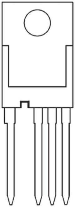
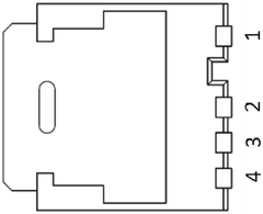
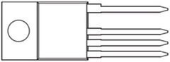
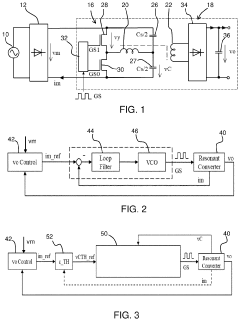
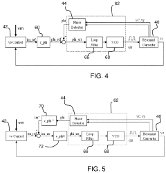
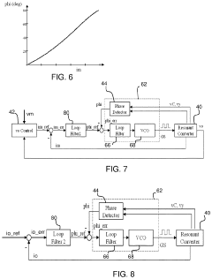
Integrated GaN power device including PFC and QR flyback controllers
PatentPendingCN120150471A
Innovation
- Using integrated gallium nitride (GaN) power devices, including power factor correction (PFC) controllers and/or quasi-resonant (QR) flyback controllers, more efficient power conversion is achieved by reducing pin count and external components.
A resonant inverter and conversion method
PatentActiveUS20230065763A1
Innovation
- A resonant inverter employing a phase modulation scheme with a phase control circuit, including a phase locked loop, to control the switch network based on phase differences between the resonant tank voltage and the phase signal, allowing for stable operation up to tens of MHz without requiring complex external circuitry.
Thermal Management Strategies for MHz-Frequency GaN Converters
Thermal management represents a critical challenge in the development of MHz-frequency GaN converters. As switching frequencies increase to the megahertz range, power losses concentrate in shorter time intervals, creating intense thermal stress on components. This phenomenon necessitates advanced cooling strategies to maintain reliable operation and prevent thermal runaway conditions.
The thermal characteristics of GaN devices differ significantly from traditional silicon counterparts. GaN's smaller die size results in higher power density, while its reduced on-resistance generates less conduction losses but potentially higher switching losses at MHz frequencies. These properties create unique thermal management requirements that conventional cooling methods struggle to address effectively.
Several innovative cooling approaches have emerged specifically for MHz-frequency GaN converters. Direct substrate cooling techniques establish thermal pathways directly from the semiconductor junction to the cooling medium, significantly reducing thermal resistance. Advanced thermal interface materials (TIMs) with enhanced thermal conductivity and reduced bond-line thickness optimize heat transfer between components and heat sinks.
Liquid cooling solutions have gained prominence in high-power density applications, offering superior heat dissipation capabilities compared to traditional air cooling. Two-phase cooling systems utilizing the latent heat of vaporization provide even greater thermal performance for the most demanding MHz-frequency applications. These systems can maintain junction temperatures within safe operating limits despite the extreme thermal challenges.
Thermal simulation and modeling tools have become essential in the design process, enabling accurate prediction of hotspots and thermal bottlenecks before physical prototyping. Computational fluid dynamics (CFD) simulations help optimize heat sink designs and airflow patterns, while electrothermal co-simulation techniques account for the interdependence between electrical performance and thermal behavior.
System-level thermal management strategies incorporate careful component placement to minimize thermal coupling between heat-generating elements. Strategic PCB design techniques, including copper pours, thermal vias, and embedded heat pipes, create efficient thermal pathways away from sensitive components. The integration of temperature sensors and dynamic thermal management algorithms allows for real-time adjustment of operating parameters to prevent thermal issues.
Recent research indicates that GaN-specific thermal management solutions can extend device lifetime by up to 40% compared to conventional approaches. As MHz-frequency converters continue to evolve, thermal management innovations will remain a primary enabler for unlocking the full potential of GaN technology in high-frequency power conversion applications.
EMI Considerations in High-Frequency GaN Applications
As GaN power devices enable PFC + LLC converters to operate at megahertz frequencies, electromagnetic interference (EMI) management becomes increasingly critical. The faster switching speeds and higher dv/dt and di/dt characteristics of GaN devices create more challenging EMI environments compared to traditional silicon-based solutions. These rapid transitions generate broadband noise that extends into higher frequency ranges, potentially affecting nearby sensitive electronics and communication systems.
The EMI profile in high-frequency GaN applications presents unique challenges in both conducted and radiated emissions. Conducted EMI typically manifests in the 150 kHz to 30 MHz range, while radiated emissions become particularly problematic above 30 MHz. With GaN-based converters operating at megahertz frequencies, significant harmonic content can extend well into the hundreds of megahertz, interfering with wireless communications bands.
Layout considerations become paramount in high-frequency GaN designs. The physical arrangement of components, trace lengths, and ground plane integrity significantly impact EMI performance. Minimizing loop areas for high-frequency current paths and implementing proper component placement can reduce parasitic inductances that exacerbate EMI issues. Studies have shown that optimized PCB layouts can reduce EMI by 10-20 dB in critical frequency bands.
Filtering strategies must evolve to address the unique EMI signature of GaN-based converters. Traditional filtering approaches designed for silicon devices often prove inadequate at megahertz frequencies. Multi-stage filters incorporating both common-mode and differential-mode elements, strategically placed closer to the noise source, demonstrate superior performance. Advanced materials such as nanocrystalline cores show promise for high-frequency EMI suppression in compact form factors.
Shielding techniques also require reconsideration for GaN applications. The higher frequency content necessitates more comprehensive shielding solutions that address both magnetic and electric field components. Selective shielding of critical circuit sections rather than entire assemblies can provide cost-effective EMI mitigation while managing thermal considerations.
Compliance with regulatory standards presents another dimension of complexity. As GaN-based power converters push into new frequency domains, designers must navigate evolving EMI regulations across different markets and applications. The CISPR 22/32 standards for information technology equipment and FCC Part 15 regulations in the US establish limits that become increasingly challenging to meet as operating frequencies increase.
Simulation tools have become essential for predicting and mitigating EMI issues in high-frequency GaN designs. Advanced electromagnetic field solvers and circuit simulators that accurately model the high-frequency behavior of GaN devices enable designers to identify potential EMI hotspots before physical prototyping, significantly reducing development cycles and compliance risks.
Unlock deeper insights with Patsnap Eureka Quick Research — get a full tech report to explore trends and direct your research. Try now!
Generate Your Research Report Instantly with AI Agent
Supercharge your innovation with Patsnap Eureka AI Agent Platform!