GaN Power Devices In Automotive Applications: Qualification, AEC-Q101, And Design Pitfalls
AUG 26, 20259 MIN READ
Generate Your Research Report Instantly with AI Agent
Patsnap Eureka helps you evaluate technical feasibility & market potential.
GaN Power Devices Evolution and Automotive Goals
Gallium Nitride (GaN) power devices have undergone significant evolution since their initial development in the early 2000s. The journey began with fundamental research on wide bandgap semiconductors, which demonstrated GaN's theoretical advantages over silicon in power applications. Early GaN devices faced challenges with substrate compatibility, reliability issues, and high production costs, limiting their commercial viability despite promising performance characteristics.
By the mid-2010s, breakthroughs in epitaxial growth techniques and device structures enabled the first generation of commercially viable GaN power transistors. These devices primarily targeted telecommunications and consumer electronics applications where efficiency advantages could justify premium pricing. The development of GaN-on-Si technology represented a pivotal advancement, dramatically reducing manufacturing costs while maintaining performance benefits.
Recent years have witnessed accelerated maturation of GaN technology, with enhanced device architectures, improved thermal management, and increased integration capabilities. The power density of GaN devices has increased by approximately 40% every two years, while costs have decreased by roughly 20% annually, following a trajectory that outpaces traditional silicon-based solutions.
In the automotive context, GaN power devices aim to address several critical goals. Primary among these is the enhancement of electric vehicle (EV) powertrain efficiency. GaN-based onboard chargers and DC-DC converters can achieve efficiency improvements of 2-3% compared to silicon alternatives, translating to extended driving range without increasing battery capacity. Size reduction represents another key objective, with GaN enabling up to 75% smaller power electronics footprints, creating valuable space savings in tightly packaged automotive systems.
Thermal performance under automotive conditions constitutes a third major goal. GaN's ability to operate efficiently at higher temperatures aligns with the automotive industry's push toward higher-temperature operation and reduced cooling requirements. The technology targets junction temperatures of 175°C or higher while maintaining reliability, compared to silicon's typical 150°C limitation.
Perhaps most critically, GaN development for automotive applications focuses on meeting stringent reliability requirements. The technology aims to achieve failure rates below 1 FIT (failures in time, or one failure per billion device-hours) and lifetimes exceeding 15 years under automotive stress conditions. This represents a significant challenge given the relatively limited field data for GaN compared to mature silicon technologies.
The roadmap for automotive GaN includes progressive qualification for increasingly demanding applications, beginning with auxiliary systems and advancing toward safety-critical powertrain components as reliability data accumulates and industry confidence grows.
Automotive Market Demand for GaN Power Solutions
The automotive industry is experiencing a significant shift towards electrification and advanced power electronics, creating substantial demand for Gallium Nitride (GaN) power solutions. This transition is primarily driven by the industry's push for higher efficiency, reduced emissions, and improved performance in electric and hybrid vehicles. Market research indicates that the automotive power electronics segment is projected to grow at a compound annual growth rate of over 30% for GaN-based solutions through 2030, substantially outpacing silicon-based alternatives.
Vehicle electrification represents the most promising application area for GaN power devices. On-board chargers (OBCs), DC-DC converters, and traction inverters all benefit from GaN's superior switching performance and efficiency. Particularly in OBCs, GaN solutions have demonstrated efficiency improvements of 3-5% compared to silicon-based systems, translating to faster charging times and reduced thermal management requirements.
The automotive industry's stringent reliability requirements have historically presented barriers to GaN adoption. However, recent advancements in GaN qualification processes aligned with AEC-Q101 standards have accelerated market acceptance. Major automotive OEMs are increasingly incorporating GaN solutions into their technology roadmaps, with several premium electric vehicle manufacturers already implementing GaN-based power systems in production models.
Range anxiety remains a critical concern for electric vehicle consumers, creating market pull for more efficient power conversion solutions. GaN devices, with their ability to operate at higher frequencies and temperatures while maintaining superior efficiency, directly address this market need by enabling smaller, lighter power systems that extend vehicle range. This alignment with consumer demands is accelerating GaN adoption across various vehicle platforms.
The transition to 800V architecture in electric vehicles represents another significant market driver for GaN power solutions. Higher voltage systems benefit disproportionately from GaN's performance characteristics, particularly in fast-charging applications where power density and efficiency are paramount. Industry forecasts suggest that by 2025, over 40% of new electric vehicle platforms will utilize 800V architecture, creating expanded opportunities for GaN implementation.
Cost considerations remain important, with automotive manufacturers seeking solutions that balance performance improvements against implementation costs. While GaN devices currently carry a price premium over silicon alternatives, the system-level benefits—including reduced cooling requirements, smaller passive components, and higher power density—are increasingly recognized as justifying the component-level cost difference, particularly in premium vehicle segments.
GaN Technology Status and Qualification Challenges
Gallium Nitride (GaN) power devices have emerged as promising alternatives to traditional silicon-based semiconductors in automotive applications due to their superior electrical properties. Currently, GaN technology is transitioning from research laboratories to commercial production, with significant advancements in manufacturing processes and reliability. The wide bandgap nature of GaN allows for higher breakdown voltages, faster switching speeds, and improved thermal performance compared to silicon counterparts.
Despite these advantages, GaN technology faces several qualification challenges in the automotive sector. The automotive industry demands stringent reliability standards, particularly through the AEC-Q101 qualification process, which was originally designed for silicon devices. This creates a fundamental challenge as GaN's different material properties and failure mechanisms require adapted qualification methodologies. The industry is actively working to develop GaN-specific qualification standards that address its unique characteristics while maintaining the rigorous requirements necessary for automotive applications.
Manufacturing consistency represents another significant challenge. Current GaN production processes exhibit higher variability compared to mature silicon technologies, leading to concerns about device-to-device performance consistency and long-term reliability. This variability impacts critical parameters such as threshold voltage, on-resistance, and breakdown characteristics, which are essential for predictable performance in automotive systems.
The qualification of GaN devices must address specific failure mechanisms not typically encountered in silicon devices. These include dynamic on-resistance degradation (current collapse), buffer trapping effects, and gate reliability issues. These phenomena can significantly impact device performance under the dynamic operating conditions typical in automotive applications, such as motor drives and DC-DC converters.
Thermal management presents additional qualification hurdles. While GaN theoretically offers better thermal performance than silicon, practical implementation in automotive environments requires careful consideration of package design and thermal interfaces. The qualification process must verify that GaN devices can maintain performance and reliability across the extreme temperature ranges experienced in automotive applications (-40°C to 150°C or higher).
Globally, qualification efforts are progressing at different rates. Japanese and European automotive manufacturers have been early adopters in qualifying GaN for specific applications, while North American companies have generally taken a more conservative approach. This geographical disparity in qualification standards and acceptance creates challenges for global supply chains and technology adoption.
The path to full qualification of GaN power devices for automotive applications requires collaborative efforts between semiconductor manufacturers, tier-one suppliers, and automotive OEMs to develop standardized testing protocols that accurately predict long-term reliability while accommodating the unique characteristics of GaN technology.
Current AEC-Q101 Qualification Approaches
01 GaN device qualification testing for automotive applications
Gallium Nitride (GaN) power devices require specific qualification testing to meet automotive standards, particularly AEC-Q101. This involves rigorous reliability testing including temperature cycling, humidity testing, mechanical stress tests, and electrical parameter verification. The qualification process ensures that GaN devices can withstand the harsh environmental conditions and operational demands of automotive applications while maintaining performance and reliability over the vehicle's lifetime.- GaN power device qualification methods for AEC-Q101 compliance: Various methods are employed to qualify GaN power devices according to AEC-Q101 standards. These methods include rigorous testing procedures such as temperature cycling, humidity testing, and high-temperature operating life tests. The qualification process ensures that GaN power devices meet the reliability requirements for automotive applications, with specific focus on parameters like gate leakage current, threshold voltage stability, and breakdown voltage under extreme conditions.
- Structural design improvements for AEC-Q101 qualified GaN devices: Specific structural design enhancements are implemented in GaN power devices to meet AEC-Q101 qualification standards. These include optimized gate structures, improved passivation layers, and enhanced thermal management solutions. The structural modifications focus on preventing common failure mechanisms such as current collapse, dynamic on-resistance degradation, and gate reliability issues, thereby ensuring the devices can withstand the stringent automotive qualification requirements.
- Testing protocols and verification systems for AEC-Q101 compliance: Specialized testing protocols and verification systems are developed for ensuring GaN power devices meet AEC-Q101 standards. These include automated test equipment configurations, customized stress test sequences, and statistical analysis methods for reliability data. The testing systems are designed to accurately measure and verify critical parameters under various operating conditions, providing comprehensive qualification data required for automotive-grade certification.
- Quality control and manufacturing processes for AEC-Q101 GaN devices: Advanced quality control methodologies and manufacturing processes are implemented to produce AEC-Q101 compliant GaN power devices. These include enhanced wafer screening techniques, in-line process monitoring, and statistical process control methods. The manufacturing approaches focus on reducing defect densities, ensuring process repeatability, and implementing traceability systems that are essential for automotive-grade semiconductor production.
- Reliability enhancement techniques for automotive GaN power devices: Various reliability enhancement techniques are employed to improve the performance and lifespan of GaN power devices in automotive applications. These techniques include buffer layer optimization, field plate engineering, and surface treatment methods. The reliability improvements address specific failure mechanisms related to high-temperature operation, voltage stress, and switching transients, ensuring the devices can meet the stringent lifetime requirements specified in AEC-Q101 standards.
02 AEC-Q101 compliance requirements for GaN power devices
AEC-Q101 compliance for GaN power devices involves meeting specific standards for stress tests, reliability, and performance metrics. These requirements include high-temperature operating life tests, temperature cycling, humidity testing, mechanical shock tests, and electrostatic discharge (ESD) protection. GaN devices must demonstrate stable electrical characteristics and reliability under extreme conditions to achieve AEC-Q101 qualification for automotive-grade applications.Expand Specific Solutions03 Manufacturing processes for automotive-qualified GaN devices
Specialized manufacturing processes are required to produce GaN power devices that meet automotive qualification standards. These processes include enhanced quality control measures, specialized substrate materials, optimized epitaxial growth techniques, and advanced packaging solutions. Manufacturing facilities must implement statistical process control and maintain traceability throughout the production chain to ensure consistent quality and reliability of GaN devices intended for automotive applications.Expand Specific Solutions04 Reliability enhancement techniques for GaN power devices
Various techniques are employed to enhance the reliability of GaN power devices to meet AEC-Q101 standards. These include optimized gate structures to prevent threshold voltage shifts, field plate designs to manage electric fields, passivation layers to protect against environmental factors, and buffer layer engineering to reduce leakage currents. Advanced packaging technologies with improved thermal management capabilities are also implemented to ensure long-term reliability under automotive operating conditions.Expand Specific Solutions05 Testing methodologies for AEC-Q101 qualification of GaN devices
Specific testing methodologies are required for AEC-Q101 qualification of GaN power devices. These include accelerated life testing, high-temperature reverse bias testing, temperature humidity bias testing, and power cycling tests. Advanced failure analysis techniques are employed to identify potential failure mechanisms and improve device design. Standardized test procedures ensure consistent evaluation of device performance and reliability across different manufacturing lots and suppliers.Expand Specific Solutions
Leading GaN Automotive Semiconductor Manufacturers
The GaN power devices market for automotive applications is in a growth phase, with increasing adoption driven by the need for higher efficiency and power density in electric vehicles. The market size is expanding rapidly as automotive manufacturers seek to improve energy efficiency and reduce carbon emissions. Technologically, GaN devices are maturing but still face challenges in meeting automotive qualification standards like AEC-Q101. Leading players include established semiconductor companies such as ON Semiconductor, STMicroelectronics, and ROHM, alongside specialized GaN-focused firms like GaN Systems and Cambridge GaN Devices. Chinese companies including Huawei and various research institutions are also making significant investments in this space. The competitive landscape is characterized by ongoing innovation in device design, packaging, and reliability testing to overcome automotive-specific challenges.
Cambridge GaN Devices Ltd.
Technical Solution: Cambridge GaN Devices (CGD) has developed a proprietary ICeGaN™ technology platform specifically for automotive applications, featuring integrated gate drive and protection circuits directly within the GaN power device. Their automotive-grade GaN HEMTs have successfully passed AEC-Q101 qualification tests, demonstrating reliability at junction temperatures up to 175°C with 1000-hour HTGB and HTRB testing. CGD's approach addresses common design pitfalls through their patented island-based architecture that eliminates parasitic effects and improves switching performance. Their devices incorporate built-in ESD protection exceeding 2kV HBM standards required for automotive applications, and feature integrated current sensing capabilities for real-time fault detection. The company has demonstrated these devices in 48V automotive systems with efficiency improvements of up to 10% compared to silicon alternatives.
Strengths: Integrated gate drive eliminates need for external components, reducing system complexity and improving reliability. Island architecture minimizes parasitic effects critical for automotive applications. Weaknesses: As a smaller company, may face challenges in manufacturing scale and supply chain compared to larger semiconductor manufacturers.
Semiconductor Components Industries LLC
Technical Solution: Semiconductor Components Industries (ON Semiconductor) has developed a comprehensive automotive-grade GaN power device portfolio based on their NexFET™ technology platform. Their devices have successfully completed rigorous AEC-Q101 qualification with extended testing protocols specifically addressing GaN reliability concerns in automotive environments, including accelerated lifetime testing under switching conditions that simulate real-world automotive applications. ON's automotive GaN solutions feature proprietary termination structures that enhance breakdown voltage stability across temperature ranges typical in automotive applications (-40°C to 175°C). Their devices incorporate specialized gate drive architectures that address the narrow gate voltage margin of GaN HEMTs, a common design pitfall in automotive implementations. ON Semiconductor has specifically addressed automotive reliability concerns through their advanced packaging technology that reduces thermal resistance by up to 30% compared to standard packages, critical for confined automotive environments with limited cooling. Their automotive reference designs include comprehensive protection schemes that address GaN-specific failure modes, including specialized current sensing and limiting circuits that respond within nanoseconds to prevent device damage during fault conditions common in automotive electrical systems.
Strengths: Extensive automotive qualification experience and established quality systems specifically for automotive-grade semiconductor manufacturing. Comprehensive design support ecosystem including simulation models validated for automotive applications. Weaknesses: Relatively later entry into the GaN market compared to some competitors may result in less field-proven reliability data specific to their GaN technology.
Critical GaN Design Considerations and Pitfalls
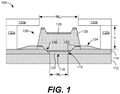
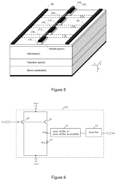
Gate metal formation on gallium nitride or aluminum gallium nitride
PatentActiveUS20210407810A1
Innovation
- A two-step process involving reactive evaporation for depositing gate metal layers, followed by sputtering of barrier and conductive metal layers to ensure complete coverage and prevent diffusion, using high barrier height metals like nickel, tungsten, and tungsten nitride to form a gate connected field plate with a hybrid gate metal approach suitable for Silicon foundries.
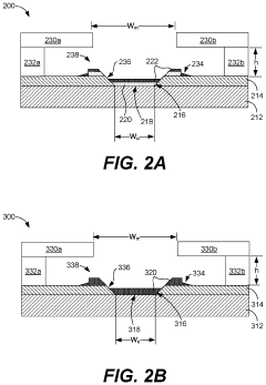
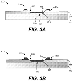
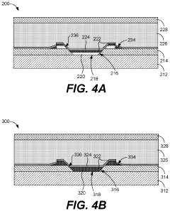
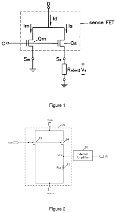
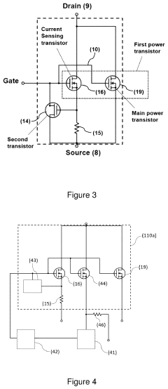
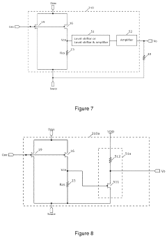
Current sensing in power semiconductor devices
PatentPendingUS20240162224A1
Innovation
- A heterojunction III-nitride high voltage/power device with a main power transistor, a sensing transistor, a resistive sensing load, and an amplifier structure that includes a level shifter and a differential amplifier, where the sensing transistor has a similar architecture to the main power transistor but with a scaled-down area or gate perimeter, and the amplifier structure provides a low VCS signal to improve linearity and accuracy while maintaining high sensitivity.
Thermal Management Strategies for Automotive GaN
Effective thermal management is critical for GaN power devices in automotive applications due to their high power density and the harsh operating environments vehicles encounter. The superior thermal conductivity of GaN compared to silicon offers inherent advantages, but automotive-grade implementations require comprehensive thermal strategies to ensure reliability under AEC-Q101 qualification standards.
Junction temperature control represents the primary thermal management challenge for automotive GaN devices. Manufacturers typically implement multi-layered approaches combining die-level, package-level, and system-level solutions. Advanced die attach materials with high thermal conductivity, such as sintered silver and copper-based composites, have demonstrated 30-40% improvement in thermal resistance compared to traditional solders.
Package-level innovations include direct bonded copper (DBC) substrates and embedded heat spreading technologies. Recent developments in double-sided cooling architectures allow heat dissipation from both top and bottom surfaces of the GaN device, reducing thermal resistance by up to 45% in automotive power modules. These advancements are particularly valuable for electric vehicle inverters where power density requirements continue to increase.
System-level thermal management incorporates liquid cooling systems, phase-change materials, and advanced thermal interface materials (TIMs). Automotive-specific TIMs must maintain performance across the -40°C to 150°C temperature range while withstanding vibration and thermal cycling. Silicone-free formulations have gained prominence due to their compatibility with automotive electronic components and long-term stability.
Computational fluid dynamics (CFD) modeling has become essential for optimizing thermal designs in automotive GaN applications. These simulations enable engineers to identify hotspots and optimize heat sink designs before physical prototyping. Transient thermal analysis is particularly important for automotive applications where load profiles vary significantly during normal vehicle operation.
Active cooling solutions, including intelligent fan control and variable-flow liquid cooling, are increasingly integrated with vehicle thermal management systems. These adaptive approaches optimize cooling performance based on real-time temperature monitoring while minimizing energy consumption. For electric vehicles, this integration extends to battery thermal management systems, creating holistic thermal solutions that balance the needs of power electronics, batteries, and cabin climate control.
The industry trend toward higher switching frequencies in GaN devices presents evolving thermal challenges, as switching losses generate additional heat that must be effectively managed. Advanced gate driver designs with precise timing control help minimize these losses, complementing physical thermal management strategies.
Reliability Testing Standards and Methodologies
Reliability testing standards for GaN power devices in automotive applications are significantly more rigorous than those for consumer electronics due to the harsh operating conditions and safety-critical nature of automotive systems. The Automotive Electronics Council's AEC-Q101 qualification standard serves as the primary framework for qualifying discrete semiconductor components, including GaN power devices. This standard encompasses a comprehensive suite of stress tests designed to evaluate device reliability under extreme conditions that simulate automotive environments.
The AEC-Q101 standard includes several critical test methodologies that GaN devices must pass. Temperature cycling tests (TC) subject devices to rapid temperature fluctuations between -55°C and 150°C for up to 1,000 cycles, evaluating the thermal expansion coefficient mismatch between different materials. High temperature reverse bias (HTRB) testing applies maximum rated voltage at elevated temperatures (typically 150°C) for 1,000 hours to assess device stability under electrical stress.
High temperature gate bias (HTGB) testing specifically evaluates the gate structure reliability by applying maximum gate voltage at elevated temperatures. This test is particularly important for GaN HEMTs due to their unique gate structures. Temperature humidity bias (THB) testing exposes devices to 85°C and 85% relative humidity under bias for 1,000 hours, assessing moisture resistance and corrosion susceptibility.
Beyond AEC-Q101, additional reliability methodologies are often employed for GaN devices. Dynamic Ron testing evaluates the increase in on-resistance during switching operations, a phenomenon particularly relevant to GaN technology. Short circuit robustness testing assesses the device's ability to withstand fault conditions without catastrophic failure, critical for automotive safety applications.
Mission profile-based testing has emerged as an advanced methodology that simulates actual application conditions rather than standardized stress tests. This approach combines multiple stress factors (temperature, humidity, vibration, electrical stress) based on the specific automotive application requirements, providing more realistic reliability predictions.
Statistical analysis methodologies like Weibull distribution analysis are increasingly utilized to extrapolate failure rates from accelerated testing data to normal operating conditions. This enables more accurate lifetime predictions and failure rate calculations, essential for meeting automotive reliability targets of less than 1 FIT (failure in time, or one failure per billion device-hours).
The implementation of these rigorous testing methodologies presents significant challenges for GaN device manufacturers but remains essential for automotive qualification. As GaN technology continues to mature, these reliability standards will likely evolve to address emerging failure mechanisms specific to wide bandgap semiconductor technologies.
Unlock deeper insights with Patsnap Eureka Quick Research — get a full tech report to explore trends and direct your research. Try now!
Generate Your Research Report Instantly with AI Agent
Supercharge your innovation with Patsnap Eureka AI Agent Platform!