GaN Power Devices For Bidirectional Converters In Energy Storage Systems
AUG 26, 202510 MIN READ
Generate Your Research Report Instantly with AI Agent
Patsnap Eureka helps you evaluate technical feasibility & market potential.
GaN Technology Evolution and Objectives
Gallium Nitride (GaN) power devices have emerged as a revolutionary technology in power electronics, offering significant advantages over traditional silicon-based semiconductors. The evolution of GaN technology began in the early 1990s with fundamental research into wide bandgap semiconductors, but commercial viability was only achieved in the 2010s. This technological progression has been driven by increasing demands for higher efficiency, smaller form factors, and better thermal performance in power conversion systems.
The fundamental advantage of GaN lies in its material properties - a wider bandgap (3.4 eV compared to silicon's 1.1 eV), higher critical electric field strength, and superior electron mobility. These characteristics enable GaN devices to operate at higher voltages, frequencies, and temperatures while maintaining efficiency. The evolution from lateral GaN-on-Si devices to more advanced vertical GaN structures represents a significant milestone in this technology's development trajectory.
For bidirectional converters in energy storage systems, GaN technology addresses several critical challenges. Traditional silicon-based converters face limitations in switching frequency, power density, and efficiency - all crucial parameters for modern energy storage applications. The evolution of GaN has specifically targeted these pain points, with recent advancements focusing on reducing on-resistance, improving thermal management, and enhancing reliability under bidirectional power flow conditions.
The primary technical objectives for GaN power devices in bidirectional converter applications include achieving breakdown voltages exceeding 650V while maintaining low on-resistance, developing packaging solutions that minimize parasitic inductances, and creating gate driver architectures optimized for high-frequency operation. Additionally, there are ongoing efforts to improve device robustness under hard-switching conditions and to enhance short-circuit withstand capabilities.
Looking forward, the technology roadmap for GaN in energy storage applications aims to further reduce costs through improved manufacturing processes and higher yields. Integration of multiple functions into single GaN chips (including protection features and sensing capabilities) represents another evolutionary path. The ultimate objective is to enable bidirectional converters that can achieve efficiencies above 99% while operating at switching frequencies of 1MHz or higher, thus dramatically reducing the size of passive components.
Industry standardization efforts are also underway to establish testing protocols and reliability benchmarks specifically for GaN devices in bidirectional applications, addressing concerns about long-term stability under the unique stress conditions of energy storage systems. These standards will be crucial for widespread adoption across various energy storage technologies, from grid-scale installations to residential battery systems.
Market Demand Analysis for Energy Storage Bidirectional Converters
The global energy storage market is experiencing unprecedented growth, driven by the increasing integration of renewable energy sources into power grids worldwide. This expansion has created a substantial demand for bidirectional converters equipped with advanced power devices such as Gallium Nitride (GaN). The market for energy storage systems is projected to reach $546 billion by 2035, with a compound annual growth rate of approximately 20% between 2023 and 2035.
Bidirectional converters represent a critical component within energy storage systems, enabling the seamless flow of power in both directions—charging and discharging—with high efficiency. The demand for these converters is particularly strong in three key segments: residential energy storage, commercial and industrial applications, and utility-scale installations. Each segment presents unique requirements regarding power ratings, efficiency, size constraints, and cost considerations.
The residential energy storage market has seen remarkable growth, with installations increasing by 138% in 2022 compared to the previous year. This surge is primarily attributed to rising electricity costs, growing concerns about grid reliability, and the increasing adoption of solar photovoltaic systems. Homeowners are increasingly seeking compact, efficient, and cost-effective bidirectional converter solutions that can maximize the value of their energy storage investments.
In the commercial and industrial sector, the demand for bidirectional converters is driven by the need to reduce peak demand charges, provide backup power, and participate in demand response programs. This segment values high power density, reliability, and advanced grid-support functionalities. The market size for commercial energy storage is expected to triple by 2027, creating substantial opportunities for GaN-based converter technologies.
Utility-scale applications represent the largest market segment by capacity, with projects typically ranging from several megawatts to gigawatt-scale installations. These systems require highly efficient, reliable, and scalable bidirectional converter solutions capable of providing grid services such as frequency regulation, voltage support, and black start capability.
Regional analysis reveals that Asia-Pacific currently leads the market, accounting for approximately 45% of global installations, followed by North America (30%) and Europe (20%). China dominates the Asia-Pacific region, driven by aggressive renewable energy targets and substantial government support for energy storage deployment.
The market is increasingly demanding converters with higher efficiency, greater power density, faster switching speeds, and enhanced reliability—all attributes that GaN power devices can potentially deliver. End-users are willing to pay premium prices for solutions that offer lower lifetime costs through reduced energy losses and extended operational lifespans, creating a favorable environment for GaN technology adoption despite higher initial costs compared to traditional silicon-based alternatives.
GaN Power Devices: Current Status and Technical Challenges
Gallium Nitride (GaN) power devices have emerged as a promising alternative to traditional silicon-based semiconductors in power electronics applications, particularly for bidirectional converters in energy storage systems. The wide bandgap properties of GaN enable higher breakdown voltages, faster switching speeds, and lower on-resistance compared to silicon counterparts, making them ideal for high-frequency, high-efficiency power conversion applications.
Currently, GaN power devices are commercially available in voltage ratings ranging from 100V to 900V, with 650V devices being the most common for energy storage applications. These devices typically achieve on-resistance values that are significantly lower than silicon MOSFETs at comparable voltage ratings, resulting in reduced conduction losses. The high electron mobility in GaN also enables switching frequencies in the MHz range, allowing for smaller passive components and increased power density.
Despite these advantages, GaN power devices face several technical challenges that limit their widespread adoption. Thermal management remains a critical issue due to the high power density and concentrated heat generation. The thermal conductivity of GaN is lower than that of silicon carbide (SiC), necessitating advanced packaging solutions to efficiently dissipate heat during high-power operation in bidirectional converters.
Reliability concerns also persist, particularly regarding dynamic RDS(on) degradation under high-voltage switching conditions. This phenomenon, where the on-resistance increases over time due to electron trapping, can significantly impact the long-term performance of GaN devices in energy storage systems that require frequent bidirectional power flow.
Gate driving presents another challenge unique to GaN technology. Unlike silicon devices, GaN HEMTs typically have lower gate threshold voltages and narrower safe operating voltage ranges. This necessitates specialized gate drivers with precise voltage control and protection features to prevent device failure during high-frequency switching operations.
Manufacturing scalability and cost remain significant barriers to widespread adoption. While GaN-on-Si technology has improved cost-effectiveness compared to native GaN substrates, production costs still exceed those of silicon devices. The complex epitaxial growth processes and specialized packaging requirements contribute to higher manufacturing expenses, limiting market penetration in cost-sensitive energy storage applications.
Integration challenges also exist when implementing GaN devices in bidirectional converter topologies. The ultrafast switching speeds, while beneficial for efficiency, create design complications related to layout parasitics, electromagnetic interference (EMI), and common-mode noise. These issues require careful circuit design and advanced PCB layout techniques to fully leverage GaN's performance advantages in bidirectional energy storage converters.
Current GaN Solutions for Bidirectional Converters
01 GaN device structure and fabrication
Gallium Nitride (GaN) power devices employ specific structural designs and fabrication techniques to enhance performance. These include specialized substrate materials, epitaxial layer structures, and manufacturing processes that optimize the electrical and thermal properties of the devices. Advanced fabrication methods help reduce defects and improve reliability, while innovative structural designs enable higher power density and efficiency in power electronic applications.- GaN device structure and fabrication: Gallium Nitride (GaN) power devices employ specific structural designs and fabrication techniques to enhance performance. These include specialized substrate materials, epitaxial layer structures, and manufacturing processes that optimize electron mobility and reduce defects. Advanced fabrication methods focus on creating reliable interfaces between GaN and other materials, improving thermal management, and enhancing overall device reliability for high-power applications.
- GaN power transistor designs: Various transistor architectures are implemented in GaN power devices to maximize efficiency and power handling capabilities. These designs include high electron mobility transistors (HEMTs), heterojunction field-effect transistors (HFETs), and enhancement-mode structures. Key innovations focus on gate design, channel engineering, and field plate configurations to achieve higher breakdown voltages, lower on-resistance, and faster switching speeds compared to conventional silicon-based devices.
- Thermal management and packaging solutions: Effective thermal management is critical for GaN power devices due to their high power density. Advanced packaging technologies and thermal dissipation strategies are employed to maintain optimal operating temperatures and prevent performance degradation. These solutions include innovative die-attach materials, integrated heat spreaders, and package designs that minimize thermal resistance while maintaining electrical performance and reliability under high-power conditions.
- GaN power conversion applications: GaN power devices are increasingly utilized in various power conversion systems due to their superior switching characteristics and efficiency. Applications include power supplies, inverters, motor drives, and renewable energy systems. The implementation of GaN technology enables higher frequency operation, reduced system size, and improved energy efficiency compared to traditional silicon-based solutions, making them particularly valuable in compact and high-efficiency power electronics.
- GaN reliability and protection mechanisms: Ensuring long-term reliability of GaN power devices requires specialized protection mechanisms and design considerations. These include strategies to mitigate dynamic on-resistance, current collapse phenomena, and gate degradation. Advanced protection circuits, robust passivation techniques, and innovative buffer layer designs are implemented to enhance device lifetime and stability under various operating conditions, particularly during high-voltage switching events and thermal cycling.
02 GaN power transistor designs
Various transistor architectures are implemented in GaN power devices to maximize performance characteristics. These include High Electron Mobility Transistors (HEMTs), heterojunction field-effect transistors, and enhancement-mode designs. These transistor configurations leverage the unique properties of GaN to achieve high breakdown voltage, low on-resistance, and fast switching speeds, making them ideal for high-frequency and high-power applications.Expand Specific Solutions03 Thermal management solutions for GaN devices
Effective thermal management is critical for GaN power devices due to their high power density. Innovations in this area include advanced packaging techniques, heat spreading materials, and thermal interface solutions that efficiently dissipate heat from the active device regions. These thermal management approaches help maintain device reliability and performance under high-power operating conditions, extending the lifetime and stability of GaN power electronics.Expand Specific Solutions04 GaN power conversion systems
GaN devices are integrated into power conversion systems such as inverters, converters, and power supplies to achieve higher efficiency and power density. These systems leverage the fast switching capabilities and low losses of GaN to operate at higher frequencies, reducing the size of passive components and enabling more compact designs. Applications include renewable energy systems, electric vehicles, and high-efficiency power supplies for consumer and industrial electronics.Expand Specific Solutions05 Reliability and protection mechanisms for GaN power devices
Ensuring long-term reliability of GaN power devices requires specialized protection mechanisms and reliability enhancement techniques. These include gate protection circuits, current limiting features, and overvoltage protection schemes tailored to the unique characteristics of GaN semiconductors. Advanced testing methodologies and lifetime prediction models help identify failure mechanisms and improve device robustness, addressing challenges such as dynamic on-resistance and threshold voltage instability.Expand Specific Solutions
Key Industry Players in GaN Power Device Manufacturing
The GaN power devices market for bidirectional converters in energy storage systems is in a growth phase, with increasing adoption driven by the superior performance of GaN over silicon. The market is expanding rapidly as energy storage becomes critical for renewable integration, with projections suggesting significant growth over the next decade. Technologically, companies like GaN Systems, Navitas Semiconductor, and InnoScience are leading commercial development with mature product offerings, while Cambridge GaN Devices and Infineon Technologies are advancing next-generation solutions. Academic institutions including Peking University and Southeast University are contributing fundamental research to overcome remaining challenges in bidirectional applications. The ecosystem shows a healthy mix of established semiconductor manufacturers and specialized GaN startups competing to optimize efficiency, reliability, and cost metrics.
GaN Systems, Inc.
Technical Solution: GaN Systems has developed a comprehensive portfolio of GaN power transistors specifically optimized for bidirectional converters in energy storage systems. Their Island Technology® design features a unique cell layout that maximizes current handling capability while minimizing on-resistance. For bidirectional applications, they've created GS-065 650V E-HEMTs with low RDS(on) (25-60mΩ) and GS-100 100V devices that enable high-frequency operation (up to 10MHz) with minimal switching losses[1]. Their GaNPX® packaging eliminates wire bonds and provides superior thermal performance, reducing junction-to-case thermal resistance to 0.5°C/W[2]. For energy storage systems, they've developed reference designs for 1-3kW bidirectional DC-DC converters achieving efficiencies exceeding 98% in both buck and boost modes[3], with power density improvements of up to 3x compared to silicon-based solutions.
Strengths: Industry-leading power density and efficiency (>98%) in bidirectional operation; excellent thermal performance through advanced packaging; comprehensive design resources including reference designs specifically for ESS applications. Weaknesses: Higher initial component cost compared to silicon alternatives; requires careful gate drive design with specific voltage requirements; thermal management still critical despite improvements.
Navitas Semiconductor Ltd.
Technical Solution: Navitas has pioneered GaNFast™ power ICs that integrate GaN power FETs with drive, control, and protection circuits in a single package, specifically addressing bidirectional converter challenges in energy storage systems. Their NV6128 platform delivers 650V capability with integrated gate drive and protection features that simplify bidirectional designs[1]. For energy storage applications, Navitas has developed bidirectional topologies achieving switching frequencies of 500kHz-1MHz, significantly reducing magnetic component size while maintaining >97% efficiency in both power flow directions[2]. Their latest generation incorporates loss-optimized dead-time control that minimizes body diode conduction losses during direction transitions. The company's GaNSense™ technology provides real-time current and temperature monitoring, enabling dynamic performance optimization and enhanced system reliability in bidirectional applications[3]. Navitas has demonstrated 3.5kW bidirectional converters for residential energy storage with power densities exceeding 70W/in³, representing a 3x improvement over silicon-based designs.
Strengths: Highly integrated solution reduces component count and simplifies design; built-in protection features enhance reliability in bidirectional applications; excellent power density achievements. Weaknesses: Integration limits flexibility in some circuit configurations; thermal management challenges in high-power applications despite integration; relatively higher cost compared to discrete solutions.
Critical Patents and Technical Innovations in GaN Power Devices
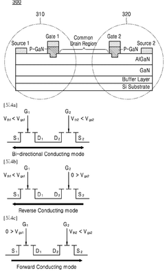
Bidirectional multi-stage gallium nitride switch and power conversion device comprising same
PatentWO2025143622A1
Innovation
- A bidirectional gallium nitride (GaN) switch is designed with a common drain or source structure, integrating two GaN switches in a single package to control bidirectional current flow, eliminating body diode losses and reducing package size.
GaN semiconductor based voltage conversion device
PatentInactiveEP1679782A2
Innovation
- A voltage converter utilizing a gallium nitride (GaN) diode with a rectifier, inductor, and output charge storage device, eliminating the need for transient voltage suppression circuits and achieving high efficiency and reduced noise.
Thermal Management Strategies for GaN-Based Converters
Thermal management represents a critical challenge in the development and deployment of GaN-based bidirectional converters for energy storage systems. The superior switching characteristics of GaN power devices, while beneficial for efficiency, generate significant thermal stress due to high power density and switching frequencies. Effective thermal management strategies are therefore essential to ensure reliable operation and maximize the performance advantages of GaN technology.
Conventional cooling methods such as forced air cooling show limitations when applied to GaN-based converters. The thermal conductivity pathway in GaN devices differs substantially from silicon counterparts, necessitating specialized approaches. Advanced thermal interface materials (TIMs) with enhanced thermal conductivity have emerged as a promising solution, with materials such as sintered silver and graphene-enhanced composites demonstrating superior performance compared to traditional thermal greases.
Direct liquid cooling techniques have gained significant traction in high-power GaN applications. Two-phase immersion cooling, where the entire converter is submerged in a dielectric fluid, has shown remarkable results in laboratory settings, achieving junction temperature reductions of up to 40°C compared to conventional methods. However, implementation challenges related to fluid maintenance and system complexity have limited widespread commercial adoption.
Integrated cooling solutions that incorporate thermal management directly into the package design represent another innovative approach. Double-sided cooling configurations, where heat is extracted from both the top and bottom of the device, have demonstrated up to 60% improvement in thermal resistance. These designs often utilize advanced substrate materials such as direct bonded copper (DBC) or active metal brazed (AMB) ceramics to enhance thermal spreading.
Computational fluid dynamics (CFD) modeling has become an indispensable tool in optimizing thermal management strategies for GaN converters. These simulations enable precise prediction of hotspots and thermal gradients, allowing designers to implement targeted cooling solutions. Recent advances in multi-physics simulation tools have further improved the accuracy of these models by accounting for the complex interactions between electrical, thermal, and mechanical domains.
Dynamic thermal management systems that adjust cooling parameters based on real-time operating conditions show particular promise for bidirectional converters in energy storage applications. These systems can optimize cooling resources during varying load conditions, significantly improving overall system efficiency while maintaining safe operating temperatures. Implementation typically involves temperature sensors, microcontrollers, and variable-speed cooling components working in concert with the power management system.
Reliability and Lifetime Assessment of GaN Power Devices
The reliability and lifetime assessment of GaN power devices is critical for their successful implementation in bidirectional converters for energy storage systems. These systems require components that can maintain performance over extended operational periods under varying stress conditions. GaN devices, while offering superior performance characteristics compared to silicon alternatives, present unique reliability challenges that must be thoroughly evaluated.
Accelerated lifetime testing has emerged as the primary methodology for assessing GaN device reliability. This approach subjects devices to elevated stress conditions—including higher temperatures, voltages, and switching frequencies—to induce failure mechanisms that would typically occur over much longer timeframes under normal operation. The resulting data enables the development of lifetime models that can predict device behavior in real-world applications.
Time-dependent dielectric breakdown (TDDB) represents one of the most significant reliability concerns for GaN power devices. This phenomenon occurs when the gate dielectric gradually degrades under electrical stress, eventually leading to catastrophic failure. Research indicates that GaN devices typically demonstrate higher TDDB resistance compared to silicon counterparts, but this advantage diminishes at elevated temperatures common in energy storage applications.
Dynamic RDS(on) degradation presents another critical reliability challenge specific to GaN technology. This effect manifests as an increase in on-resistance during switching operations, potentially compromising the efficiency benefits that make GaN attractive for bidirectional converters. Recent studies have shown that this degradation can be mitigated through optimized device structures and improved packaging techniques that better manage thermal dissipation.
Thermal cycling resilience is particularly relevant for energy storage systems that experience frequent charge-discharge cycles. GaN devices must withstand repeated thermal expansion and contraction without developing microcracks or delamination at material interfaces. Advanced packaging solutions incorporating sintered silver or copper interconnects have demonstrated superior thermal cycling performance compared to traditional solder-based approaches.
Mission profile-based lifetime estimation has gained prominence as a more accurate approach to reliability assessment. This methodology incorporates actual application conditions—including load profiles, ambient temperature variations, and operational cycles—to provide more realistic lifetime predictions than traditional constant-stress testing. For bidirectional converters in energy storage systems, these profiles must account for both charging and discharging operational modes.
Field reliability data, though still limited due to the relatively recent commercial deployment of GaN technology, has begun to validate laboratory assessments. Early implementations in renewable energy systems suggest that properly designed GaN-based converters can achieve failure rates comparable to silicon solutions while delivering significant performance advantages.
Unlock deeper insights with Patsnap Eureka Quick Research — get a full tech report to explore trends and direct your research. Try now!
Generate Your Research Report Instantly with AI Agent
Supercharge your innovation with Patsnap Eureka AI Agent Platform!