Package Comparison For GaN Power Devices: QFN, LGA, And Flip-Chip
AUG 26, 20259 MIN READ
Generate Your Research Report Instantly with AI Agent
Patsnap Eureka helps you evaluate technical feasibility & market potential.
GaN Power Device Packaging Evolution and Objectives
Gallium Nitride (GaN) power devices have emerged as a revolutionary technology in power electronics, offering superior performance compared to traditional silicon-based solutions. The evolution of GaN power device packaging has been a critical factor in the widespread adoption and commercialization of this technology. Initially, GaN power devices utilized conventional packaging technologies borrowed from silicon power devices, which limited their performance potential due to parasitic inductances and thermal constraints.
The packaging evolution for GaN power devices began in the early 2000s with traditional through-hole packages, progressing to surface-mount options as the technology matured. A significant milestone occurred around 2010 when specialized packages designed specifically for GaN's unique characteristics began to emerge, addressing the need for higher switching frequencies and better thermal management.
Three packaging technologies have become predominant in the GaN power device market: Quad Flat No-lead (QFN), Land Grid Array (LGA), and Flip-Chip. Each represents a different stage in the evolutionary path of GaN packaging solutions, with progressive improvements in electrical performance, thermal management, and reliability.
QFN packages, an early adoption for GaN devices, offered improved thermal performance through exposed pads but still suffered from wire bond-related parasitic inductances. LGA packages emerged as an intermediate solution, providing better electrical performance through shorter interconnection paths while maintaining relatively straightforward manufacturing processes.
The flip-chip technology represents the most advanced packaging solution currently available for GaN power devices, virtually eliminating wire bonds and significantly reducing parasitic inductances, thereby enabling GaN devices to operate closer to their theoretical performance limits.
The primary objectives driving GaN packaging evolution include minimizing parasitic inductances to enable higher switching frequencies, improving thermal management to handle GaN's high power density, enhancing reliability under high-temperature and high-frequency operation, and reducing manufacturing costs to compete with silicon alternatives.
Future packaging evolution aims to achieve even higher levels of integration, incorporating multiple GaN devices and their associated drive and protection circuits into single packages. This system-in-package approach is expected to further enhance performance while simplifying system design. Additionally, research is focused on developing packaging solutions that can withstand higher operating temperatures, approaching 250°C, to fully leverage GaN's wide bandgap advantages.
The industry is also exploring advanced substrate materials and interconnection technologies to further reduce thermal resistance and parasitic elements, pushing GaN devices closer to their theoretical performance limits while ensuring long-term reliability in demanding applications.
Market Demand Analysis for Advanced GaN Packaging Solutions
The global market for GaN power devices is experiencing robust growth, driven primarily by the increasing demand for high-efficiency power electronics across multiple industries. Current market valuations place the GaN power device market at approximately 1.4 billion USD in 2023, with projections indicating a compound annual growth rate (CAGR) of 25-30% through 2030. This accelerated growth trajectory is significantly outpacing traditional silicon-based power semiconductors, which typically see single-digit growth rates.
Advanced packaging solutions for GaN devices represent a critical component of this market expansion. Industry analysis indicates that packaging can constitute up to 70% of the total device cost, making packaging innovation a key differentiator in competitive positioning. The demand for QFN (Quad Flat No-leads), LGA (Land Grid Array), and Flip-Chip packaging solutions is being shaped by several converging market forces.
The automotive sector has emerged as a primary demand driver, particularly with the rapid adoption of electric vehicles (EVs). The EV charging infrastructure market alone is expected to grow at 30% CAGR through 2028, creating substantial demand for high-performance GaN packages that can handle increased power density requirements. Automotive-grade reliability standards are pushing manufacturers toward LGA and enhanced QFN packages that offer superior thermal performance and reliability.
Consumer electronics represents another significant market segment, with manufacturers seeking smaller form factors and higher efficiency in power adapters, wireless chargers, and audio equipment. This sector shows particular interest in flip-chip packaging solutions due to their reduced parasitic inductance and improved thermal characteristics, enabling the development of more compact and efficient consumer devices.
The telecommunications infrastructure sector, particularly with the ongoing 5G deployment, has created substantial demand for GaN RF devices with advanced packaging. Base station power amplifiers require packages that can handle high frequencies while maintaining thermal stability, making flip-chip and specialized LGA packages increasingly popular in this segment.
Industrial power conversion applications are gravitating toward QFN and LGA packages due to their balance of cost-effectiveness and performance. The industrial automation market, growing at approximately 10% annually, requires robust packaging solutions that can withstand harsh operating environments while delivering high reliability.
Regional analysis reveals that Asia-Pacific dominates the market demand for advanced GaN packaging, accounting for over 60% of global consumption, followed by North America and Europe. This regional distribution aligns with the concentration of electronics manufacturing and automotive production facilities.
Customer requirements are increasingly focused on packages that enable higher switching frequencies (beyond 1 MHz), lower inductance (sub-nH range), and improved thermal management (capable of handling junction temperatures up to 175°C). These technical demands are directly influencing packaging selection and development priorities across the industry.
Current Packaging Technologies and Thermal Management Challenges
GaN power devices are currently packaged using three primary technologies: QFN (Quad Flat No-leads), LGA (Land Grid Array), and Flip-Chip. Each packaging solution presents distinct advantages and challenges, particularly in thermal management which is critical for high-power applications.
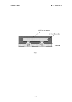
QFN packages represent the most traditional approach, featuring a lead frame structure with exposed thermal pad on the bottom. This design allows for direct soldering to PCB thermal vias, providing a primary heat dissipation path. However, QFN packages face limitations in thermal resistance, typically ranging from 8-15°C/W, which becomes problematic as GaN power densities increase. The package's wire bonding connections also introduce parasitic inductances that can limit high-frequency performance.
LGA packages offer improved thermal performance through their planar structure with multiple connection points on the bottom surface. The absence of leads reduces parasitic inductances and allows for more efficient heat spreading. Thermal resistance values for LGA packages typically range from 5-10°C/W, representing a significant improvement over QFN. Additionally, LGA packages enable smaller form factors while maintaining robust mechanical stability.
Flip-Chip technology represents the most advanced packaging solution currently available for GaN devices. By directly connecting the active die face-down to the substrate using solder bumps, flip-chip eliminates wire bonds entirely. This configuration dramatically reduces thermal resistance to as low as 2-4°C/W and minimizes parasitic inductances. The direct thermal path from junction to case significantly enhances cooling efficiency, making flip-chip particularly suitable for high-power density applications.
A major challenge across all packaging technologies is managing the thermal interface materials (TIMs) between the package and heat sink. Current TIMs exhibit thermal conductivities ranging from 3-10 W/m·K, creating a thermal bottleneck in the overall system. Industry research is actively pursuing advanced TIM solutions with conductivities exceeding 20 W/m·K.
Another significant challenge is addressing thermal expansion coefficient mismatches between GaN dies, package materials, and PCB substrates. These mismatches create mechanical stresses during thermal cycling that can lead to reliability issues, particularly in flip-chip packages where the rigid connections provide less stress relief than wire bonds.
Double-sided cooling approaches are emerging as promising solutions for ultra-high-power applications. These designs incorporate thermal pathways both above and below the die, potentially reducing thermal resistance by 30-50% compared to single-sided cooling. However, implementation challenges remain regarding manufacturability and cost-effectiveness at scale.
Comparative Analysis of QFN, LGA, and Flip-Chip Implementations
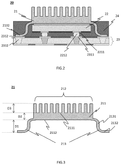
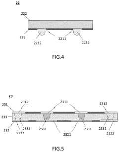
01 QFN packaging for GaN power devices
Quad Flat No-lead (QFN) packaging is widely used for GaN power devices due to its excellent thermal performance and compact footprint. This packaging technology features a exposed die pad on the bottom surface that enhances heat dissipation, which is crucial for high-power GaN devices. The QFN package also offers low parasitic inductance and resistance, improving the switching performance of GaN power devices. The design typically includes copper leadframes and specialized thermal interface materials to optimize heat transfer from the GaN die to the PCB.- QFN packaging for GaN power devices: Quad Flat No-lead (QFN) packaging is widely used for GaN power devices due to its excellent thermal performance and compact form factor. This packaging technology features a flat lead frame with exposed die pad for enhanced heat dissipation, which is critical for high-power GaN applications. The QFN package allows for reduced parasitic inductance and resistance, improving the overall electrical performance of GaN power devices. The design typically incorporates copper lead frames and optimized thermal paths to manage the high heat generation of GaN devices.
- LGA packaging solutions for GaN devices: Land Grid Array (LGA) packaging provides superior electrical and thermal performance for GaN power devices. This packaging technology features a flat contact pad array instead of pins or balls, offering excellent thermal conductivity and electrical connectivity. LGA packages for GaN devices typically incorporate advanced thermal management solutions such as integrated heat spreaders or direct bonded copper substrates. The low-profile nature of LGA packages makes them suitable for space-constrained applications while maintaining the high performance requirements of GaN power devices.
- Flip-chip technology for GaN power applications: Flip-chip packaging technology offers significant advantages for GaN power devices by eliminating wire bonds and directly connecting the device to the substrate through solder bumps or copper pillars. This configuration substantially reduces parasitic inductance and thermal resistance, enabling higher switching frequencies and improved thermal management. The flip-chip approach allows for more efficient heat dissipation paths and smaller form factors compared to traditional wire-bonded packages. Advanced flip-chip designs may incorporate through-silicon vias (TSVs) or embedded heat sinks to further enhance thermal performance.
- Thermal management solutions in GaN packaging: Effective thermal management is critical for GaN power device packaging due to the high power density and heat generation. Advanced packaging solutions incorporate innovative thermal management techniques such as integrated heat spreaders, thermal vias, and specialized thermal interface materials. Some designs feature direct bonded copper or aluminum nitride substrates to maximize heat dissipation. Double-sided cooling approaches are also employed in advanced packages, where heat is removed from both the top and bottom of the device. These thermal management solutions are essential for maintaining device reliability and performance under high-power operating conditions.
- Novel packaging architectures for GaN power devices: Innovative packaging architectures are being developed specifically for GaN power devices to address their unique requirements. These include embedded die technologies where the GaN device is integrated within the PCB material, chip-scale packages that approach the theoretical minimum size, and multi-chip modules that combine GaN with silicon devices. Some novel approaches incorporate advanced interconnect technologies such as silver sintering or transient liquid phase bonding for improved reliability. These packaging innovations aim to maximize the inherent benefits of GaN technology while addressing challenges related to parasitics, thermal management, and electromagnetic interference.
02 LGA packaging solutions for GaN semiconductors
Land Grid Array (LGA) packaging provides superior electrical and thermal performance for GaN power devices. The LGA structure features an array of conductive pads on the bottom of the package that connect directly to the PCB without protruding leads. This configuration minimizes the package's parasitic inductance, which is critical for high-frequency GaN applications. LGA packages for GaN devices often incorporate advanced thermal management solutions, including integrated heat spreaders and specialized die-attach materials, to handle the high power density of GaN semiconductors while maintaining reliability under thermal stress.Expand Specific Solutions03 Flip-chip technology for GaN device packaging
Flip-chip packaging technology offers significant advantages for GaN power devices by connecting the semiconductor die directly to the substrate using conductive bumps rather than wire bonds. This architecture substantially reduces parasitic inductance and resistance, enabling higher switching frequencies and improved efficiency. The direct thermal path from the active junction to the package exterior enhances heat dissipation capabilities, which is essential for high-power GaN applications. Advanced flip-chip designs incorporate specialized underfill materials to manage coefficient of thermal expansion mismatches and improve reliability under thermal cycling conditions.Expand Specific Solutions04 Thermal management solutions in GaN power packages
Effective thermal management is critical for GaN power device packaging due to the high power density and operating temperatures. Advanced packaging solutions incorporate specialized thermal interface materials, embedded heat spreaders, and innovative die-attach technologies to maximize heat dissipation. Some designs feature direct bonded copper (DBC) substrates or insulated metal substrates (IMS) to improve thermal conductivity from the GaN die to the heat sink. Double-sided cooling architectures are also employed in high-performance packages to further enhance thermal performance, allowing GaN devices to operate at higher power levels without compromising reliability or lifetime.Expand Specific Solutions05 Advanced interconnect technologies for GaN packages
Innovative interconnect technologies are being developed specifically for GaN power device packaging to minimize parasitic elements and improve electrical performance. These include copper clip bonding, which replaces traditional aluminum wire bonds with a solid copper connector to reduce resistance and inductance while improving thermal performance. Silver sintering is increasingly used as an alternative to conventional solder materials, offering superior thermal conductivity and reliability at high temperatures. Some advanced packages also incorporate embedded die technology, where the GaN device is integrated directly within the PCB substrate, minimizing interconnect distances and optimizing electrical and thermal performance.Expand Specific Solutions
Critical Patents and Innovations in GaN Package Design
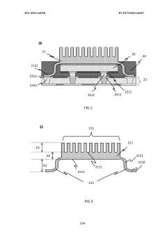
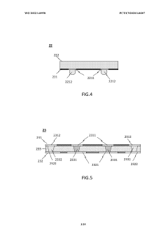
Semiconductor package and method for manufacturing
PatentWO2022140958A1
Innovation
- Development of a FC-LGA package with enhanced heat dissipation capability specifically designed for GaN power devices to overcome thermal limitations.
- Optimization of package architecture to minimize parasitic inductance while maximizing thermal conductivity path from GaN device junction to ambient environment.
- Cost-effective alternative to expensive SiC substrates while maintaining comparable thermal performance for GaN power devices.
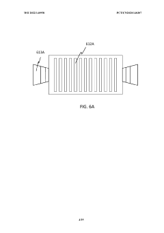
Semiconductor Package and Method for Manufacturing the Same
PatentActiveUS20220375815A1
Innovation
- A semiconductor package design incorporating a heatsink with thermally conductive vias and heat dissipation fins, where the heatsink is mounted on the semiconductor die with dissipation leads connected to the substrate, and an encapsulation layer covers the leads while exposing the fins for enhanced thermal conductivity and reduced packaging size.


Reliability and Qualification Standards for GaN Packages
Reliability and qualification standards for GaN packages are critical considerations in the adoption of GaN power devices across various applications. The industry has established specific testing protocols that address the unique characteristics and failure mechanisms of GaN semiconductors, which differ significantly from traditional silicon-based devices.
JEDEC standards form the foundation of qualification requirements for GaN packages, with JESD22 series providing comprehensive testing methodologies. These standards have been adapted to address GaN-specific concerns, including thermal performance under high-frequency switching conditions and reliability at elevated temperatures.
For QFN packages, qualification typically focuses on thermal cycling (JESD22-A104), temperature-humidity-bias testing (JESD22-A101), and high-temperature operating life tests (JESD22-A108). The thermal resistance path in QFN packages requires particular attention due to GaN's higher power density compared to silicon devices.
LGA packages undergo similar qualification procedures but with additional emphasis on mechanical stress testing due to their land grid interface. Warpage testing becomes especially important as LGA packages for GaN applications often feature thinner profiles to optimize thermal performance, making them more susceptible to mechanical stresses during assembly.
Flip-chip packages require the most rigorous qualification standards, including specialized tests for bump integrity and underfill reliability. The direct die-attach method necessitates careful evaluation of coefficient of thermal expansion (CTE) mismatches between the GaN die and substrate materials, with thermal cycling tests often extended to higher cycle counts.
Automotive-grade GaN devices face even more stringent requirements, with AEC-Q101 qualification mandatory for all package types. This includes extended high-temperature testing (up to 175°C for Grade 0), power and temperature cycling, and humidity testing under bias conditions.
Industry trends show movement toward standardized reliability metrics specific to GaN technology, with organizations like JEDEC and AEC working to develop GaN-specific qualification standards. These emerging standards address unique failure mechanisms such as dynamic RDS(on) degradation and threshold voltage shifts that are particularly relevant to GaN HEMT structures.
Package-specific qualification data indicates that flip-chip designs generally demonstrate superior reliability in high-temperature cycling tests, while QFN packages show advantages in humidity resistance due to their simpler structure and established molding compounds. LGA packages typically offer a balance between the reliability aspects of both alternatives.
Cost-Performance Tradeoffs in GaN Packaging Selection
When selecting packaging solutions for GaN power devices, manufacturers and engineers must carefully evaluate the cost-performance tradeoffs between QFN, LGA, and flip-chip options. Each packaging technology presents distinct economic considerations that directly impact both production expenses and device performance characteristics.
QFN (Quad Flat No-lead) packages typically offer the most cost-effective solution among the three options, with established manufacturing processes that benefit from economies of scale. The simplified structure and mature assembly techniques result in lower production costs, making QFN packages particularly attractive for consumer electronics and cost-sensitive applications. However, this cost advantage comes with thermal and electrical performance limitations that may necessitate additional system-level cooling solutions, potentially offsetting initial savings.
LGA (Land Grid Array) packages represent a middle-ground approach, balancing moderate manufacturing costs with improved thermal and electrical performance. The increased production complexity compared to QFN results in approximately 15-25% higher packaging costs, but delivers superior power density capabilities. This makes LGA packages suitable for industrial applications where performance requirements justify the additional expense but extreme performance is not necessary.
Flip-chip technology stands at the premium end of the spectrum, commanding significantly higher costs—often 40-60% more than QFN solutions—due to complex manufacturing processes and specialized equipment requirements. The advanced interconnection method eliminates bond wires, dramatically reducing parasitic inductance and improving thermal performance. Despite the higher initial investment, flip-chip packaging can enable system-level cost reductions through increased power density, reduced cooling requirements, and improved reliability in high-stress environments.
The selection process must also consider volume requirements and production scale. At high volumes, the per-unit cost differential between packaging options narrows, potentially making premium solutions more economically viable. Conversely, for low-volume specialized applications, the initial tooling and setup costs for advanced packaging may prove prohibitive.
Long-term reliability considerations further complicate the cost-performance equation. While flip-chip packages typically demonstrate superior reliability metrics in harsh environments, potentially reducing warranty and replacement costs, QFN packages may require additional protection measures that increase system-level expenses. The total cost of ownership, including maintenance and operational efficiency over the product lifecycle, often favors more advanced packaging solutions despite higher initial procurement costs.
Unlock deeper insights with Patsnap Eureka Quick Research — get a full tech report to explore trends and direct your research. Try now!
Generate Your Research Report Instantly with AI Agent
Supercharge your innovation with Patsnap Eureka AI Agent Platform!