Thermal Management Strategies For GaN Power Devices In Closed-Frame Chargers
AUG 26, 20259 MIN READ
Generate Your Research Report Instantly with AI Agent
Patsnap Eureka helps you evaluate technical feasibility & market potential.
GaN Power Device Thermal Challenges and Objectives
Gallium Nitride (GaN) power devices have emerged as a revolutionary technology in power electronics, offering significant advantages over traditional silicon-based semiconductors. These wide-bandgap devices provide higher efficiency, faster switching speeds, and greater power density, making them increasingly popular in applications such as closed-frame chargers. However, the thermal management of GaN devices presents unique challenges that must be addressed to fully realize their potential.
The evolution of power electronics has been marked by a continuous pursuit of higher efficiency and smaller form factors. GaN technology represents a significant leap forward in this journey, with theoretical performance limits far exceeding those of silicon. The thermal characteristics of GaN, however, introduce complexities that require innovative management strategies, particularly in confined spaces like closed-frame chargers where heat dissipation pathways are limited.
Historically, thermal management for power devices has relied on conventional approaches such as heatsinks, fans, and thermal interface materials. As power densities increase with GaN adoption, these traditional methods are reaching their practical limits, necessitating new thermal solutions specifically tailored to GaN's unique properties and operating conditions.
The primary objective of thermal management for GaN devices is to maintain junction temperatures below critical thresholds while maximizing power density. This balance is particularly challenging in closed-frame chargers where space constraints limit cooling options. Effective thermal strategies must address not only steady-state operation but also transient thermal events that can cause reliability issues over time.
Another critical goal is to develop cost-effective thermal solutions that don't negate the size and efficiency advantages that GaN offers. This requires a holistic approach that considers the entire thermal path from the GaN die to the ambient environment, optimizing each interface and component along this path.
The industry is increasingly focused on developing integrated thermal management solutions that combine multiple cooling technologies. These hybrid approaches aim to address the specific thermal characteristics of GaN, including its higher thermal conductivity but lower maximum operating temperature compared to silicon carbide alternatives.
Looking forward, the technical roadmap for GaN thermal management must address several key objectives: reducing thermal resistance in package designs, developing advanced thermal interface materials compatible with GaN's unique properties, creating more efficient cooling structures for confined spaces, and implementing intelligent thermal management systems that can adapt to varying operating conditions.
Market Demand Analysis for Compact High-Efficiency Chargers
The global market for compact high-efficiency chargers has experienced exponential growth over the past decade, primarily driven by the proliferation of portable electronic devices and the increasing consumer demand for faster charging solutions. The adoption of GaN power devices in closed-frame chargers represents a significant technological advancement that addresses these market needs, offering superior power density and efficiency compared to traditional silicon-based solutions.
Consumer electronics manufacturers are increasingly prioritizing smaller form factors for charging devices while simultaneously demanding higher power outputs. Market research indicates that the global fast charger market reached $6.3 billion in 2022 and is projected to grow at a CAGR of 13.2% through 2028. This growth trajectory is particularly pronounced in the smartphone and laptop segments, where consumers are willing to pay premium prices for chargers that deliver rapid charging capabilities in compact designs.
The automotive sector presents another substantial market opportunity, with electric vehicle (EV) manufacturers seeking more efficient and compact onboard charging solutions. The EV charger market alone is expected to reach $27.5 billion by 2027, with a significant portion dedicated to high-efficiency solutions that can reduce charging times and improve overall energy utilization.
Corporate sustainability initiatives and regulatory pressures are further accelerating market demand for energy-efficient charging solutions. The European Union's implementation of common charging standards and energy efficiency requirements has created a regulatory environment that favors advanced thermal management technologies in GaN-based chargers. Similarly, the U.S. Department of Energy's efficiency standards are pushing manufacturers toward more efficient power conversion solutions.
Consumer behavior studies reveal that charging speed and device size are among the top five purchasing considerations for mobile accessories. A 2023 consumer survey showed that 78% of smartphone users consider fast charging capability "very important" or "extremely important" when purchasing new devices or accessories, representing a significant shift from just 45% five years ago.
The enterprise market segment shows particular promise, with businesses increasingly investing in charging infrastructure to support remote and hybrid work environments. Corporate procurement of high-efficiency chargers grew by 34% in 2022, reflecting the need to equip employees with reliable, space-efficient charging solutions for multiple devices.
Asian markets, particularly China, Japan, and South Korea, currently lead in adoption of advanced charging technologies, accounting for approximately 62% of global market share. However, North American and European markets are showing accelerated growth rates of 15.7% and 14.3% respectively, indicating expanding global demand for this technology.
Current Thermal Management Limitations in Closed-Frame Designs
Closed-frame chargers present significant thermal management challenges for GaN power devices due to their compact design and limited airflow. These chargers typically feature enclosed plastic or metal housings that restrict heat dissipation pathways, creating thermal bottlenecks that can severely impact device performance and reliability. The primary limitation stems from the confined space, which prevents the implementation of traditional cooling solutions such as large heatsinks or active cooling systems.
The thermal conductivity of materials used in closed-frame designs presents another critical limitation. Standard FR-4 PCB materials offer thermal conductivity values of only 0.3-0.5 W/m·K, creating significant thermal resistance in the heat dissipation path. While metal-core PCBs provide improved thermal performance (typically 1-3 W/m·K), their implementation in compact chargers often faces cost and manufacturing constraints.
Interface thermal resistance represents a substantial challenge in these designs. The thermal interface materials (TIMs) currently employed between GaN devices and heatsinks or chassis often exhibit thermal resistances of 0.5-2°C·cm²/W, creating bottlenecks in the thermal pathway. This resistance becomes particularly problematic as power densities increase in next-generation GaN-based chargers.
Current closed-frame designs also struggle with thermal spreading limitations. The concentrated heat generated by GaN devices creates localized hotspots that are difficult to dissipate effectively within confined spaces. Thermal simulations indicate that temperature gradients of 15-30°C can develop across small PCB areas, significantly reducing overall thermal performance.
The absence of effective airflow within closed-frame chargers exacerbates these issues. Natural convection cooling becomes highly restricted, with typical heat transfer coefficients limited to 5-10 W/m²·K, compared to 20-100 W/m²·K achievable with forced convection. This limitation forces designs to rely heavily on conduction pathways, which are already constrained by the factors mentioned above.
Thermal cycling and reliability concerns further complicate the thermal management landscape. GaN devices in closed-frame chargers experience significant temperature fluctuations during operation, with thermal cycles potentially exceeding 50°C. These cycles create mechanical stresses at material interfaces, leading to degradation of thermal interface materials and solder joints over time, further compromising thermal performance.
The miniaturization trend in consumer electronics continues to push power densities higher while reducing available thermal management space. Current closed-frame designs struggle to maintain junction temperatures below the recommended 150°C threshold for GaN devices when power densities exceed 40-50 W/in³, creating a fundamental limitation for further size reduction without innovative thermal solutions.
Existing Thermal Dissipation Techniques for Confined Spaces
01 Heat dissipation structures for GaN power devices
Various heat dissipation structures can be implemented in GaN power devices to manage thermal issues. These include specialized heat sinks, thermal interface materials, and innovative package designs that facilitate efficient heat transfer away from the GaN chip. Such structures are critical for maintaining optimal operating temperatures and preventing thermal runaway conditions that could degrade device performance or cause failure.- Heat Sink and Thermal Interface Materials: Advanced heat sink designs and thermal interface materials are crucial for GaN power device thermal management. These solutions include specialized heat sink structures with optimized fin designs, advanced thermal interface materials that reduce thermal resistance between the GaN device and heat sink, and composite materials with enhanced thermal conductivity. These approaches effectively dissipate heat from GaN power devices, maintaining optimal operating temperatures and improving device reliability and performance.
- Package-Level Thermal Solutions: Package-level thermal management solutions for GaN power devices include innovative package designs that optimize heat flow paths, embedded heat spreaders within the package structure, and direct die-attach techniques that minimize thermal resistance. These approaches focus on improving the thermal pathway from the GaN die to the external environment, reducing junction temperatures and enhancing overall thermal performance of the packaged device.
- Active Cooling Technologies: Active cooling technologies for GaN power devices include liquid cooling systems with microchannels, thermoelectric cooling elements integrated with GaN devices, and forced-air cooling solutions specifically designed for high-power GaN applications. These active cooling approaches provide enhanced heat removal capabilities compared to passive solutions, enabling GaN devices to operate at higher power densities while maintaining safe operating temperatures.
- Substrate and Material Innovations: Innovations in substrate materials and device structures significantly impact thermal management of GaN power devices. These include diamond-based substrates with superior thermal conductivity, engineered substrate materials with reduced thermal boundary resistance, and novel buffer layer designs that optimize heat dissipation. These material innovations address thermal challenges at the device level, improving heat spreading and reducing thermal bottlenecks in GaN power devices.
- System-Level Thermal Design: System-level thermal management approaches for GaN power devices include optimized PCB designs with thermal vias and embedded cooling layers, power electronics modules with integrated cooling solutions, and thermal management systems that coordinate multiple cooling mechanisms. These comprehensive approaches consider the entire thermal path from the GaN device through the system, enabling efficient heat removal and thermal stability in high-power applications.
02 Substrate materials and configurations for thermal management
The choice of substrate material and configuration significantly impacts thermal management in GaN power devices. Materials with high thermal conductivity such as silicon carbide (SiC), diamond, or advanced composite substrates can effectively dissipate heat generated during operation. Various substrate configurations, including flip-chip designs and through-substrate vias, can be employed to optimize thermal pathways and reduce thermal resistance.Expand Specific Solutions03 Integration of cooling systems with GaN devices
Advanced cooling systems can be integrated with GaN power devices to enhance thermal management. These include liquid cooling solutions, microfluidic channels, vapor chambers, and two-phase cooling technologies. Such cooling systems can be directly integrated into the device package or implemented at the system level to efficiently remove heat from high-power GaN devices operating under demanding conditions.Expand Specific Solutions04 Thermal management in multi-chip GaN power modules
Multi-chip GaN power modules present unique thermal management challenges due to higher power densities and potential thermal coupling between devices. Specialized thermal management approaches for these modules include optimized chip placement, thermal balancing techniques, shared cooling structures, and advanced packaging technologies that minimize thermal resistance between multiple GaN chips and the cooling system.Expand Specific Solutions05 Thermal simulation and modeling for GaN device design
Thermal simulation and modeling techniques are essential for optimizing the thermal management of GaN power devices. Advanced computational fluid dynamics (CFD), finite element analysis (FEA), and multi-physics simulation tools enable designers to predict thermal behavior, identify hotspots, and evaluate various cooling strategies before physical implementation. These approaches help in developing more thermally efficient GaN power devices and systems.Expand Specific Solutions
Key Industry Players in GaN Power Solutions
The thermal management landscape for GaN power devices in closed-frame chargers is evolving rapidly, currently in a growth phase with market projections exceeding $2 billion by 2026. While the technology is advancing beyond early adoption, it remains in mid-maturity with significant innovation potential. Key players demonstrate varied approaches: GaN Systems and Navitas lead with specialized thermal solutions, while established semiconductor manufacturers like STMicroelectronics and Analog Devices integrate GaN into broader portfolios. Academic institutions including Xidian University and UESTC contribute fundamental research, creating a competitive ecosystem where thermal innovation directly impacts device performance, reliability, and market adoption in increasingly compact charging applications.
GaN Systems, Inc.
Technical Solution: GaN Systems has developed comprehensive thermal management solutions specifically for GaN power devices in closed-frame chargers. Their approach includes advanced packaging technologies with optimized thermal interfaces that reduce junction-to-case thermal resistance to below 0.5°C/W. The company employs a multi-level thermal management strategy incorporating direct copper bonding (DCB) substrates with thermal vias that facilitate efficient heat dissipation from the GaN die to the heatsink. Their patented Island Technology® creates a cell layout that optimizes current handling while minimizing heat concentration. For closed-frame applications, they've developed specialized thermal interface materials (TIMs) with thermal conductivity exceeding 5 W/m·K that maintain performance over the device lifetime. GaN Systems also implements active cooling solutions using miniaturized, high-efficiency fans with intelligent thermal control algorithms that adjust cooling based on real-time temperature monitoring, allowing for dynamic thermal management in space-constrained closed-frame designs.
Strengths: Industry-leading thermal resistance values enable higher power density in compact designs. Their Island Technology® provides superior current distribution, reducing hotspots. Comprehensive system-level approach addresses multiple thermal pathways simultaneously. Weaknesses: Solutions may require more complex manufacturing processes, potentially increasing production costs. Some advanced cooling solutions increase system complexity and potential points of failure.
Murata Manufacturing Co. Ltd.
Technical Solution: Murata has pioneered an integrated thermal management approach for GaN devices in closed-frame chargers focusing on material innovation and structural optimization. Their solution incorporates high thermal conductivity ceramic substrates (aluminum nitride with thermal conductivity >170 W/m·K) that serve as both electrical insulators and efficient thermal conductors. Murata's design employs a layered cooling architecture with embedded phase-change materials that absorb thermal energy during peak loads and release it during lower power operation, effectively dampening thermal transients. Their closed-frame chargers feature specially designed internal air channels that create guided convection currents, enhancing passive cooling efficiency without external airflow. Murata has also developed proprietary thermal interface materials with nano-particle fillers that reduce thermal boundary resistance at critical interfaces by up to 40% compared to conventional materials. The company's thermal simulation capabilities allow for precise optimization of component placement and thermal path design, resulting in maximum heat dissipation within extremely compact form factors.
Strengths: Advanced ceramic substrate technology provides excellent thermal performance while maintaining electrical isolation. Phase-change material integration offers superior handling of transient thermal loads. Comprehensive thermal simulation capabilities enable optimized designs. Weaknesses: High-performance ceramic substrates increase component costs. Complex internal air channel designs may complicate manufacturing and assembly processes.
Critical Patents in GaN Device Cooling Technologies
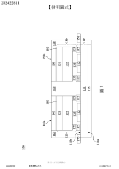
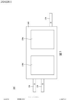
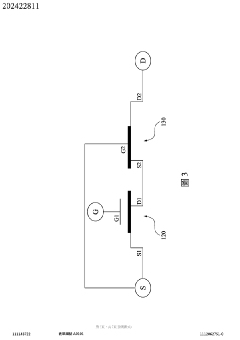
Gallium nitride power device
PatentActiveTW202422811A
Innovation
- A gallium nitride power component design featuring a ceramic metal composite circuit substrate with thermally conductive metal pads and layers, separating electrical and thermal pathways, and utilizing double-sided heat dissipation through metal thermal conductive layers to manage heat effectively.

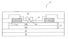
Gallium Nitride Material Devices and Thermal Designs Thereof
PatentActiveUS20100140665A1
Innovation
- The design involves arranging transistors in cells with optimized spacing and staggered configurations, along with thermally conductive packaging and selective substrate removal to enhance heat conduction, including the use of vias and thermally conductive material regions to improve thermal resistance.
Material Science Advancements for Thermal Interfaces
Recent advancements in material science have revolutionized thermal interface materials (TIMs) for GaN power devices in closed-frame chargers. Traditional TIMs such as thermal greases and pads are being supplemented or replaced by novel materials with significantly enhanced thermal conductivity properties. Graphene-based TIMs have emerged as particularly promising, offering thermal conductivity values exceeding 2000 W/m·K in-plane and up to 10 W/m·K through-plane, substantially outperforming conventional silicone-based materials that typically achieve only 1-5 W/m·K.
Carbon nanotube (CNT) arrays represent another breakthrough, with vertically aligned structures providing thermal conductivity of 15-20 W/m·K while maintaining compliance necessary for interface applications. These materials effectively bridge microscopic air gaps between contact surfaces, dramatically reducing thermal contact resistance in the confined spaces of closed-frame chargers.
Phase change materials (PCMs) have evolved to incorporate nanoparticle enhancements, creating composite materials that melt at specific operating temperatures (typically 45-70°C) to fill surface irregularities while maintaining position stability. These advanced PCMs offer thermal conductivities of 3-8 W/m·K, significantly higher than their predecessors.
Metal-based TIMs utilizing liquid metal alloys (primarily gallium-based) provide exceptional thermal conductivity of 20-80 W/m·K. Recent innovations have addressed historical challenges of electrical conductivity and potential corrosion through encapsulation techniques and surface treatments, making these materials increasingly viable for GaN applications.
Ceramic-filled polymers represent a balance between performance and practicality, with boron nitride and aluminum oxide fillers increasing thermal conductivity to 8-12 W/m·K while maintaining electrical insulation properties critical for power electronics. Advanced dispersion techniques have improved filler loading beyond 80% by volume without compromising mechanical properties.
Aerogel-based TIMs offer promising solutions for extreme miniaturization scenarios, with their ultralow density (0.003-0.15 g/cm³) and competitive thermal conductivity (0.5-2 W/m·K). Their superior thermal performance under compression makes them particularly suitable for the high-pressure contact points common in compact charger designs.
These material advancements collectively address the critical thermal bottleneck at interfaces between GaN devices and heat sinks in closed-frame chargers, enabling higher power densities while maintaining reliability. The selection of optimal TIM technology increasingly depends on specific application parameters including power profile, form factor constraints, and cost considerations.
Reliability and Safety Standards for High-Power Density Chargers
The reliability and safety standards for high-power density chargers have become increasingly stringent as GaN technology enables more compact designs with higher power capabilities. International standards bodies including IEC, UL, and IEEE have established comprehensive frameworks that manufacturers must adhere to when developing closed-frame chargers utilizing GaN power devices.
Temperature-related safety standards are particularly critical for GaN implementations, with most regulations requiring automatic thermal shutdown mechanisms that activate when internal temperatures exceed predetermined thresholds—typically between 125°C and 150°C depending on the specific standard. These protective measures must demonstrate reliability through accelerated life testing protocols that simulate years of operation under various thermal stress conditions.
Electrical safety standards have evolved specifically to address the unique characteristics of GaN devices, including their faster switching speeds and potential for electromagnetic interference. Standards such as IEC 62368-1 now include specific provisions for wide-bandgap semiconductor devices, mandating enhanced isolation barriers and more robust overvoltage protection systems for chargers operating at high power densities.
Certification processes for high-power density GaN chargers require comprehensive documentation of thermal management strategies, including detailed thermal simulations, infrared thermal imaging results, and physical testing data. Regulatory bodies increasingly demand evidence that thermal solutions remain effective throughout the product's expected lifetime, even after thousands of thermal cycles.
Material selection for thermal management components must comply with flammability ratings specified in standards like UL 94, with most high-power applications requiring V-0 rated materials at minimum. Additionally, the thermal interface materials must maintain their properties within specified temperature ranges while meeting environmental compliance regulations such as RoHS and REACH.
Failure mode and effects analysis (FMEA) specific to thermal management has become a mandatory element in safety certification, requiring manufacturers to identify potential thermal failure scenarios and implement appropriate mitigation strategies. This analysis must demonstrate that no single-point thermal failure can lead to unsafe conditions or fire hazards.
Recent updates to international standards have introduced more stringent requirements for thermal cycling endurance, reflecting the understanding that GaN-based chargers in consumer electronics experience frequent power cycling that can accelerate thermal fatigue. Current standards typically require devices to withstand 5,000-10,000 thermal cycles without significant degradation in thermal performance or safety features.
Unlock deeper insights with Patsnap Eureka Quick Research — get a full tech report to explore trends and direct your research. Try now!
Generate Your Research Report Instantly with AI Agent
Supercharge your innovation with Patsnap Eureka AI Agent Platform!