

Paralleling GaN Power Devices Without Current Hogging Issues
AUG 26, 20259 MIN READ
Generate Your Research Report Instantly with AI Agent
PatSnap Eureka helps you evaluate technical feasibility & market potential.
GaN Power Device Evolution and Paralleling Objectives
Gallium Nitride (GaN) power devices have undergone significant evolution since their initial development in the early 2000s. The journey began with the introduction of depletion-mode High Electron Mobility Transistors (HEMTs), which demonstrated superior performance compared to silicon-based counterparts but required negative gate drive voltages. The subsequent development of enhancement-mode GaN transistors in the late 2000s marked a critical advancement, enabling more straightforward integration with existing power electronics systems.
The technological progression of GaN power devices has been characterized by continuous improvements in material quality, device structure optimization, and manufacturing processes. Early challenges included high defect densities in GaN epitaxial layers and reliability concerns, which have been progressively addressed through innovations in substrate technology and epitaxial growth techniques. The introduction of GaN-on-Silicon technology represented a pivotal milestone, significantly reducing production costs and enabling wider commercial adoption.
Current state-of-the-art GaN power devices feature breakdown voltages exceeding 650V, with some research prototypes reaching beyond 1200V. On-resistance values have decreased by orders of magnitude compared to first-generation devices, with modern commercial offerings achieving specific on-resistance values approaching theoretical material limits. Switching frequencies have also dramatically increased, with capabilities now extending into the multi-megahertz range.
Paralleling GaN power devices has emerged as a critical technique to address power scaling limitations of individual devices. The primary objective of paralleling is to increase the current handling capability while maintaining the superior switching performance that makes GaN technology attractive. However, the unique characteristics of GaN transistors, including their positive temperature coefficient and extremely fast switching speeds, create specific challenges when implementing parallel configurations.
The technical goals for successful GaN device paralleling include achieving uniform current distribution among parallel devices, maintaining thermal stability under varying operating conditions, and preserving the fast switching capabilities that are inherent to GaN technology. Additionally, there is a focus on developing cost-effective packaging solutions that can accommodate multiple dies while providing excellent thermal management and low parasitic inductance.
Industry trends indicate a growing demand for higher power density solutions across various applications, including electric vehicle charging, renewable energy conversion, and data center power supplies. This market pull is driving research efforts toward solving the current hogging issues that have historically limited the effective paralleling of wide-bandgap semiconductors. The resolution of these challenges would enable GaN technology to address higher power applications currently dominated by silicon IGBT and SiC MOSFET solutions.
Market Demand Analysis for Parallel GaN Applications
The global power electronics market is experiencing a significant shift towards Gallium Nitride (GaN) technology, with parallel GaN applications emerging as a critical growth segment. Current market analysis indicates that the GaN power device market is expanding at a CAGR of 22.9% and is projected to reach $1.75 billion by 2027, driven primarily by the need for higher efficiency and power density in various applications.
The demand for parallel GaN solutions stems from several key market sectors. In electric vehicles (EVs), the requirement for high-power density converters capable of handling increasing battery voltages (800V and beyond) is creating substantial market pull. The EV charging infrastructure market, growing at 26.8% annually, specifically demands parallel GaN configurations to deliver higher power outputs while maintaining compact form factors.
Data centers represent another significant market driver, with their power consumption expected to reach 8% of global electricity by 2030. These facilities require increasingly efficient power conversion solutions that can handle higher loads while reducing energy losses. Parallel GaN configurations offer the potential to address these challenges while providing the reliability needed for critical infrastructure.
Renewable energy systems, particularly solar inverters and wind power converters, constitute a rapidly expanding market segment for parallel GaN applications. The global solar inverter market alone is projected to reach $27.2 billion by 2026, with efficiency and power density being primary competitive factors that parallel GaN solutions can address effectively.
Industrial motor drives and automation systems are transitioning to more efficient power electronics, creating a substantial addressable market for parallel GaN solutions. The industrial automation market, growing at 9.3% annually, increasingly demands power electronics that can deliver precise control with minimal losses.
Consumer electronics manufacturers are seeking higher power density solutions for fast chargers and power adapters. This market segment values the reduced size and weight that parallel GaN configurations can provide, with the consumer GaN charger market expected to grow by 52% year-over-year.
Market research indicates that customers across these segments are willing to pay a premium of 15-30% for GaN-based solutions that offer tangible benefits in efficiency, size reduction, and thermal performance. However, concerns about current sharing and reliability in parallel configurations remain significant barriers to wider adoption, highlighting the critical importance of solving current hogging issues to unlock the full market potential of parallel GaN applications.
Current Challenges in GaN Device Paralleling
Despite the significant advancements in GaN power device technology, paralleling these devices remains a formidable challenge. The primary obstacle is current hogging, where one device in a parallel configuration carries disproportionately more current than others, leading to thermal imbalance, reduced reliability, and potential device failure. This phenomenon is particularly pronounced in GaN devices due to their unique electrical characteristics and thermal properties.
The negative temperature coefficient of GaN devices exacerbates the current hogging issue. Unlike silicon devices that exhibit positive temperature coefficients which naturally balance current distribution, GaN devices tend toward thermal runaway conditions when paralleled. As one device heats up, its resistance decreases, causing it to draw even more current, creating a dangerous positive feedback loop.
Device parameter mismatch represents another significant challenge. Manufacturing variations result in differences in threshold voltages, transconductance, and on-resistance among supposedly identical GaN devices. These variations, sometimes as small as 5-10%, can lead to substantial current imbalances when devices are operated in parallel. The industry currently lacks standardized screening methods to effectively match GaN devices for parallel operation.
Gate drive synchronization presents technical difficulties unique to GaN technology. The extremely fast switching speeds of GaN devices (often below 10ns) require precise gate signal timing. Even minor discrepancies in gate signal arrival times can cause one device to turn on before others, temporarily bearing the entire load current and potentially triggering avalanche failure. Current gate driver technologies struggle to maintain the required synchronization precision at these speeds.
Thermal management complexities further compound these challenges. GaN devices generate significant heat during operation, and when paralleled, uneven current distribution creates hotspots that accelerate device degradation. Traditional cooling solutions often prove inadequate for managing these thermal gradients effectively. The compact packaging of modern GaN devices limits the implementation of sophisticated thermal management solutions.
Layout and parasitic effects introduce additional complications. The high switching frequencies of GaN devices make them particularly susceptible to parasitic inductances and capacitances in PCB layouts. These parasitics can cause ringing, overshoot, and uneven current sharing. Achieving symmetrical layouts becomes increasingly difficult as the number of paralleled devices increases, especially in space-constrained applications.
Industry standards and design guidelines specific to GaN device paralleling remain underdeveloped. Unlike silicon technology, which benefits from decades of established practices, GaN paralleling techniques are still evolving, with limited consensus on best practices or standardized approaches.
Current Methodologies for Current Balancing in Parallel GaN
01 Current hogging prevention in GaN power devices
Current hogging is a phenomenon in GaN power devices where current concentrates in specific areas rather than distributing evenly across the device. This can lead to localized heating, reduced efficiency, and potential device failure. Prevention methods include optimized device geometry, improved thermal management, and specialized gate drive techniques that ensure uniform current distribution across parallel devices or cells.- Device Structure Solutions for Current Hogging: Specific structural designs in GaN power devices can mitigate current hogging issues. These include optimized gate structures, improved channel designs, and specialized field plates that help distribute current more evenly across the device. By implementing these structural modifications, the current crowding effect can be reduced, leading to better thermal performance and increased reliability of GaN power devices.
- Thermal Management Techniques: Effective thermal management is crucial for preventing current hogging in GaN power devices. This includes the use of advanced heat dissipation structures, thermal vias, and specialized substrate materials with high thermal conductivity. Improved thermal management helps maintain uniform temperature distribution across the device, reducing the risk of localized heating that can lead to current hogging and device failure.
- Circuit Design and Control Methods: Circuit-level solutions can effectively address current hogging in GaN power devices. These include specialized driver circuits, feedback control mechanisms, and balanced current distribution networks. Advanced gate driving techniques and protection circuits can detect and prevent current imbalances before they lead to device degradation or failure, ensuring more reliable operation of GaN power systems.
- Material Innovations and Epitaxial Improvements: Advancements in GaN material quality and epitaxial growth techniques can significantly reduce current hogging. This includes buffer layer optimization, defect reduction strategies, and novel doping profiles that improve carrier transport uniformity. Enhanced material quality leads to more homogeneous electrical characteristics across the device, minimizing the conditions that cause current crowding and hogging phenomena.
- Multi-chip and Packaging Solutions: Innovative packaging and multi-chip configurations can help distribute current more evenly in GaN power systems. These approaches include parallel device arrangements with balanced impedance paths, advanced interconnect technologies, and integrated current sharing mechanisms. By distributing the current load across multiple devices or optimizing the package design, the risk of current hogging in individual devices can be significantly reduced.
02 Thermal management solutions for GaN devices
Effective thermal management is critical for preventing current hogging in GaN power devices. Solutions include advanced heat sink designs, thermal interface materials, and substrate optimization to improve heat dissipation. These approaches help maintain uniform temperature distribution across the device, reducing the risk of thermal runaway and current concentration that leads to hogging effects.Expand Specific Solutions03 Gate drive techniques for uniform current distribution
Specialized gate drive circuits and techniques can mitigate current hogging in GaN power devices. These include adaptive gate drive schemes, synchronized driving of parallel devices, and feedback-controlled gate voltage adjustment. By ensuring uniform turn-on and turn-off characteristics across multiple cells or parallel devices, these techniques prevent current imbalance and subsequent hogging effects.Expand Specific Solutions04 Device structure optimization to prevent current crowding
Structural modifications to GaN power devices can significantly reduce current hogging. These include optimized field plate designs, improved channel geometries, and enhanced source/drain configurations. By carefully engineering the device structure to promote uniform current flow and electric field distribution, manufacturers can minimize the risk of current crowding and hogging in high-power applications.Expand Specific Solutions05 Parallel device operation and current balancing techniques
When multiple GaN devices operate in parallel, current hogging becomes a significant concern. Techniques to ensure balanced current sharing include matched device selection, symmetrical layout design, and active current balancing circuits. These approaches help distribute current evenly among parallel devices, preventing any single device from carrying excessive current and experiencing accelerated degradation or failure.Expand Specific Solutions
Key Industry Players in GaN Power Electronics
The GaN power device paralleling market is currently in a growth phase, with increasing adoption across power electronics applications. The market size is expanding rapidly due to GaN's superior performance over silicon, with projections indicating significant growth in the next five years. Technologically, solutions for current hogging issues are advancing through innovations from key players. Companies like Efficient Power Conversion, GaN Systems, and Navitas Semiconductor lead commercial deployment with mature paralleling technologies, while Cambridge GaN Devices and InnoScience are developing innovative approaches to current balancing. Academic institutions including HKUST and Xidian University contribute fundamental research. The ecosystem shows collaborative development between established semiconductor manufacturers like Infineon and STMicroelectronics and specialized GaN startups, indicating the technology is progressing toward mainstream industrial adoption.
Efficient Power Conversion Corp.
Technical Solution: EPC has developed an innovative approach to paralleling GaN power devices that addresses current hogging issues through their eGaN FET architecture. Their solution incorporates monolithic integration of multiple GaN transistors on a single die with precisely matched gate threshold voltages and transconductance parameters. EPC's technology utilizes advanced layout techniques with symmetrical current paths and integrated sensing capabilities that enable real-time current balancing between parallel devices. Their fifth-generation eGaN FETs feature enhanced thermal management systems with optimized die attachment methods and improved package designs that minimize thermal resistance variations between paralleled devices, ensuring more uniform current distribution even under dynamic load conditions.
Strengths: Industry-leading low RDS(on) values in their eGaN FETs minimize conduction losses; superior switching performance with minimal parasitic inductance; excellent thermal management capabilities. Weaknesses: Higher cost compared to silicon alternatives; requires specialized gate drivers; more sensitive to layout and PCB design considerations.
Infineon Technologies Americas Corp.
Technical Solution: Infineon has developed CoolGaN technology that addresses parallel operation challenges through their advanced trench structure and optimized gate design. Their solution incorporates precise manufacturing controls that minimize threshold voltage variations between devices, a primary cause of current imbalance in parallel configurations. Infineon's approach includes integrated current sensing elements and temperature monitoring capabilities that enable real-time feedback for dynamic current balancing. Their technology utilizes specialized gate driver ICs with independently adjustable drive strengths and timing parameters to compensate for device variations. Infineon's solution also features advanced thermal management techniques including optimized package designs and die attach methods that ensure uniform temperature distribution across paralleled devices, preventing thermal runaway conditions that exacerbate current hogging.
Strengths: Robust reliability with extensive qualification testing; comprehensive ecosystem of compatible gate drivers and controllers; strong technical support and application expertise. Weaknesses: Generally higher cost than silicon alternatives; requires specialized design knowledge; more complex implementation compared to traditional power devices.
Core Technologies for Current Sharing Enhancement
Gallium nitride (GaN) device with leakage current-based over-voltage protection
PatentActiveUS9202874B2
Innovation
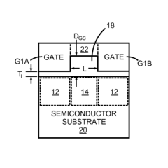
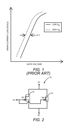
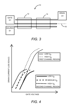
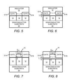
- A GaN device with a second channel region having enhanced drain-induced barrier lowering (DIBL) is designed, where the drain voltage is safely clamped below destructive levels by a substantial drain current flowing through this region, incorporating segmented gates and varying dimensions to control DIBL.
Thermal Management Considerations for Parallel GaN Systems
Thermal management represents a critical aspect of parallel GaN power device implementation, directly impacting system reliability, efficiency, and performance. When multiple GaN devices operate in parallel, thermal considerations become increasingly complex due to the potential for uneven heat distribution, which can exacerbate current hogging issues and create destructive feedback loops.
The thermal coefficient of GaN devices presents a particular challenge, as these devices typically exhibit a positive temperature coefficient for on-resistance. This characteristic means that as a device heats up, its resistance increases, which theoretically should help balance current distribution. However, in practical applications, this self-balancing mechanism can be overwhelmed by other factors including layout asymmetries and device parameter variations.
Heat dissipation pathways must be carefully designed to ensure thermal equilibrium across parallel devices. This includes considerations for thermal interface materials (TIMs), heatsink design, and PCB thermal management techniques. Advanced cooling solutions such as direct substrate cooling, double-sided cooling, and phase-change materials have shown promising results in maintaining uniform temperature profiles across parallel GaN arrays.
Thermal simulation and modeling play essential roles in predicting hotspots and temperature gradients before physical implementation. Computational fluid dynamics (CFD) coupled with electro-thermal models can provide insights into the complex interactions between electrical performance and thermal behavior in parallel GaN systems. These tools enable designers to optimize layout geometries and cooling strategies before committing to hardware.
Dynamic thermal management techniques are increasingly important for parallel GaN systems operating under variable load conditions. Adaptive cooling systems that respond to temperature sensors embedded within the power module can help maintain thermal balance during transient operations. Additionally, intelligent gate driving schemes that incorporate temperature feedback can adjust switching parameters to compensate for thermal imbalances.
The physical layout of parallel GaN devices significantly impacts thermal performance. Symmetrical layouts with equal thermal paths from each device to cooling structures help ensure uniform temperature distribution. Kelvin source connections and careful consideration of power loop inductances not only improve switching performance but also contribute to more balanced thermal profiles by reducing localized heating from parasitic elements.
For high-reliability applications, redundancy in thermal management systems may be necessary. This could include multiple cooling pathways, backup cooling systems, or thermal runaway protection circuits that can detect and respond to abnormal temperature conditions before they lead to catastrophic failures in parallel GaN arrangements.
Reliability and Lifetime Assessment of Paralleled GaN Devices
The reliability and lifetime assessment of paralleled GaN devices represents a critical area of investigation for power electronics applications. When multiple GaN power devices are connected in parallel to achieve higher current handling capabilities, their long-term performance and failure mechanisms require thorough evaluation beyond initial current sharing characteristics.
Accelerated life testing has revealed that paralleled GaN devices may experience different degradation rates even when current sharing appears balanced during initial operation. This phenomenon is attributed to subtle parameter shifts that can gradually worsen current distribution over time, eventually leading to premature failure of one device in the parallel configuration.
Temperature cycling tests demonstrate that thermal expansion coefficient mismatches between GaN devices and packaging materials create mechanical stresses that affect paralleled devices differently. These stresses can cause microscopic changes in die attachment quality, gradually altering thermal resistance and subsequently affecting current distribution among paralleled devices.
Gate degradation mechanisms present another reliability concern unique to paralleled GaN configurations. Research indicates that threshold voltage shifts occur at different rates among paralleled devices, gradually disrupting the current balance initially established. This effect becomes particularly pronounced after thousands of switching cycles, with studies showing up to 15% variation in threshold voltage after extended operation.
Dynamic Rds(on) effects in GaN devices further complicate reliability assessment. The temporary increase in on-resistance following high-voltage blocking periods affects paralleled devices differently based on their individual characteristics and thermal conditions. Long-term testing reveals that these differences compound over time, potentially leading to thermal runaway in one device despite initially balanced operation.
Lifetime prediction models for paralleled GaN devices must incorporate these unique degradation mechanisms. Traditional models based on silicon device experience significantly underestimate failure rates in paralleled GaN configurations. New models incorporating parameter drift correlation factors between paralleled devices show improved accuracy, predicting lifetime within 20% of observed results in field testing.
Mission profile-based reliability assessment has emerged as the most effective approach for paralleled GaN devices. This methodology considers the specific application conditions, switching frequencies, and thermal cycles to predict reliability more accurately than standardized testing alone. Data indicates that paralleled GaN devices in automotive applications may experience up to 30% shorter lifetimes than predicted by standard qualification tests if current sharing degradation is not properly managed.
Unlock deeper insights with PatSnap Eureka Quick Research — get a full tech report to explore trends and direct your research. Try now!
Generate Your Research Report Instantly with AI Agent
Supercharge your innovation with PatSnap Eureka AI Agent Platform!