Failure Modes Of GaN Power Devices Under Surge And Transient Conditions
AUG 26, 20259 MIN READ
Generate Your Research Report Instantly with AI Agent
Patsnap Eureka helps you evaluate technical feasibility & market potential.
GaN Power Device Evolution and Research Objectives
Gallium Nitride (GaN) power devices have emerged as revolutionary components in power electronics, offering significant advantages over traditional silicon-based technologies. The evolution of GaN power devices began in the early 2000s with fundamental research into wide bandgap semiconductors. These early investigations revealed GaN's exceptional properties, including higher breakdown voltage, faster switching speeds, and lower on-resistance compared to silicon counterparts.
The technological trajectory of GaN power devices has been marked by several key milestones. Initially, lateral GaN high-electron-mobility transistors (HEMTs) dominated the landscape, primarily developed for RF applications. Around 2010, researchers began adapting these structures specifically for power electronics applications, leading to the development of enhancement-mode GaN transistors that could operate safely in power conversion systems.
Between 2010 and 2015, significant advancements were made in substrate technology, moving from expensive silicon carbide substrates to more cost-effective GaN-on-Silicon approaches. This transition represented a crucial turning point, making GaN power devices commercially viable for broader market adoption while maintaining their performance advantages.
Recent years have witnessed accelerated development in device architecture and manufacturing processes. The introduction of p-GaN gate structures, field plates, and advanced passivation techniques has substantially improved device reliability and performance under normal operating conditions. However, the behavior of these devices under surge and transient conditions remains an area requiring deeper investigation.
The primary research objectives in this domain focus on understanding the fundamental failure mechanisms of GaN power devices when subjected to electrical overstress, voltage surges, and other transient events. These conditions are particularly relevant in industrial applications, automotive systems, and renewable energy installations where power fluctuations are common.
Specifically, research aims to characterize how different GaN device architectures respond to surge events, identify the physical degradation mechanisms at the material and device level, and develop predictive models for device lifetime under various stress conditions. Understanding the time-dependent dielectric breakdown, dynamic Ron degradation, and thermal runaway mechanisms during surge events represents a critical knowledge gap.
Additionally, research objectives include developing standardized testing methodologies for GaN reliability under transient conditions, as current testing protocols derived from silicon technology may not adequately address GaN's unique characteristics. The ultimate goal is to establish design guidelines and protection strategies that can enhance the robustness of GaN power devices in real-world applications where transient electrical events are unavoidable.
Market Demand Analysis for Robust GaN Power Electronics
The global market for GaN power devices is experiencing robust growth driven by increasing demand for high-efficiency power electronics across multiple sectors. Current market valuations indicate the GaN power device market reached approximately 223 million USD in 2022, with projections suggesting a compound annual growth rate (CAGR) of 25-30% through 2030, potentially reaching 2.5 billion USD.
This accelerated growth stems primarily from the automotive sector's transition toward electric vehicles, where GaN devices offer significant advantages in onboard chargers, DC-DC converters, and traction inverters. The automotive segment alone is expected to grow at 35% CAGR, representing nearly 40% of the total GaN power device market by 2028.
Consumer electronics constitutes another substantial market segment, with fast chargers for mobile devices and laptops driving adoption. This segment has seen particularly strong demand for GaN-based solutions that deliver higher power density in smaller form factors, with manufacturers reporting 50-70% size reductions compared to silicon-based alternatives.
Industrial applications represent the third major market driver, with increasing implementation in motor drives, industrial power supplies, and renewable energy systems. The industrial segment values reliability under harsh operating conditions, creating specific demand for GaN devices with enhanced robustness against transient events and power surges.
Market research indicates that reliability concerns under surge and transient conditions remain a significant barrier to wider adoption. A recent industry survey revealed that 78% of power system designers cite concerns about GaN reliability under abnormal operating conditions as a primary hesitation factor when considering GaN implementation.
Regional analysis shows Asia-Pacific leading GaN power device adoption, accounting for approximately 45% of global market share, followed by North America (30%) and Europe (20%). China, Japan, and South Korea are particularly aggressive in developing domestic GaN supply chains, with government initiatives supporting research into reliability enhancement.
The market demonstrates clear willingness to pay premium prices for GaN solutions with proven robustness against transient events. Products with demonstrated surge immunity command 15-25% price premiums over standard GaN offerings, indicating strong market demand for solutions addressing these failure modes.
Customer requirements increasingly specify surge and transient performance metrics in procurement specifications, with 65% of enterprise-level customers now including specific surge immunity requirements in their component qualification processes.
Current Challenges in GaN Reliability Under Transient Conditions
Despite significant advancements in Gallium Nitride (GaN) power device technology, reliability under surge and transient conditions remains a critical challenge that impedes widespread commercial adoption. Current GaN devices exhibit vulnerability to various failure mechanisms when subjected to electrical overstress events, including short-circuit conditions, voltage spikes, and lightning surges. These transient events can trigger catastrophic failures that are not adequately addressed by conventional reliability testing frameworks designed for silicon devices.
A primary challenge is the limited understanding of GaN-specific failure physics under extreme transient conditions. Unlike silicon devices with decades of reliability data, GaN power devices exhibit unique degradation mechanisms due to their wide bandgap properties and heterogeneous material structure. The high electric fields sustainable in GaN materials create distinctive breakdown mechanisms that are not fully characterized, particularly at the GaN/AlGaN interface and near gate structures.
Thermal management during transient events presents another significant challenge. GaN devices can experience localized hotspots that reach critical temperatures within nanoseconds during surge events, far faster than silicon counterparts. The thermal conductivity limitations of GaN substrates and packaging materials exacerbate this issue, creating thermal runaway conditions that accelerate device degradation and failure.
Current reliability testing methodologies are inadequate for accurately predicting GaN device behavior under transient conditions. Standard qualification procedures like JEDEC tests were primarily developed for silicon technologies and fail to capture GaN-specific failure modes. This testing gap creates uncertainty in lifetime predictions and hampers the development of robust design guidelines for GaN power applications.
The dynamic Ron phenomenon (current collapse) represents a particularly challenging reliability issue under transient conditions. When subjected to high-voltage switching events, GaN devices can experience temporary increases in on-resistance due to charge trapping effects, significantly impacting performance in power conversion applications. This phenomenon becomes more pronounced under surge conditions and can accelerate long-term degradation.
Manufacturing consistency also remains problematic for GaN reliability. Process variations in epitaxial growth, gate formation, and passivation layers create device-to-device variability in transient robustness. This inconsistency complicates the establishment of universal design rules and safety margins for GaN power systems.
Additionally, there is limited field data on GaN device failures in real-world applications, particularly under extreme environmental conditions or grid anomalies. This knowledge gap between laboratory testing and actual deployment scenarios creates uncertainty in reliability predictions and hinders the development of effective protection strategies for GaN-based power systems.
Current Surge Protection Solutions for GaN Devices
01 Thermal management and heat dissipation failures
GaN power devices are susceptible to thermal management issues that can lead to device failure. Excessive heat generation during operation can cause degradation of the semiconductor material, affecting device performance and reliability. Proper heat dissipation structures and thermal management solutions are critical to prevent overheating and subsequent failure modes such as thermal runaway or material degradation. Advanced cooling techniques and package designs are implemented to mitigate these thermal-related failure mechanisms.- Thermal management and heat dissipation failures: GaN power devices are susceptible to thermal management issues that can lead to device failure. Excessive heat generation during operation can cause degradation of the semiconductor material, affecting device performance and reliability. Proper heat dissipation structures and thermal management solutions are critical to prevent overheating and subsequent failure modes such as thermal runaway or material degradation. Advanced cooling techniques and package designs are implemented to mitigate these thermal-related failure mechanisms.
- Gate degradation and dielectric breakdown: Gate-related failures are common in GaN power devices, including gate leakage current increase, threshold voltage shifts, and dielectric breakdown. These failures can occur due to high electric fields, charge trapping at the interface, or material defects in the gate structure. The degradation of the gate dielectric over time can lead to catastrophic device failure or gradual performance deterioration. Improved gate stack designs and materials are being developed to enhance the reliability and robustness of GaN power devices against these failure mechanisms.
- Current collapse and dynamic RON degradation: Current collapse and dynamic on-resistance (RON) degradation are significant reliability concerns in GaN power devices. These phenomena occur due to charge trapping effects at the surface or in the buffer layers during high-voltage switching operations. The trapped charges create a virtual gate that depletes the channel, increasing resistance and reducing current capability. This degradation mechanism affects the switching performance and efficiency of GaN power devices, particularly in high-frequency applications. Various passivation techniques and buffer layer optimizations are employed to mitigate these effects.
- Package-related failures and interconnect reliability: The packaging of GaN power devices presents unique challenges that can lead to failure modes. These include die attach degradation, wire bond fatigue, solder joint cracking, and delamination between different package materials. The coefficient of thermal expansion mismatch between GaN and packaging materials can induce mechanical stress during thermal cycling, leading to package integrity issues. Advanced packaging technologies, including flip-chip bonding and embedded die techniques, are being developed to improve the reliability of GaN power device interconnections and reduce package-related failures.
- Buffer layer defects and substrate-related failures: Defects in the buffer layers and substrate-related issues can significantly impact GaN power device reliability. These include dislocations, cracks, and impurities that propagate from the substrate through the epitaxial layers. Such defects can create leakage paths, reduce breakdown voltage, and cause premature device failure. The quality of the substrate material and the growth conditions of the buffer layers are critical factors affecting device performance and reliability. Advanced epitaxial growth techniques and defect management strategies are being implemented to minimize these substrate and buffer-related failure modes.
02 Gate degradation and dielectric breakdown
Gate-related failures are common in GaN power devices, including gate leakage current increase, threshold voltage shifts, and dielectric breakdown. These failures can occur due to high electric fields, charge trapping at interfaces, or material defects in the gate stack. Over time, these mechanisms lead to degraded switching performance, increased power losses, and eventual device failure. Improved gate dielectric materials and optimized gate structures are being developed to enhance reliability and prevent premature breakdown.Expand Specific Solutions03 Current collapse and dynamic RON degradation
Current collapse and dynamic on-resistance (RON) increase are significant reliability concerns in GaN power devices. These phenomena occur due to charge trapping effects at surface states or in buffer layers during high-voltage switching operations. The trapped charges create a virtual gate that depletes the channel, increasing resistance and reducing current capability during transient operations. This degradation mechanism affects switching performance and efficiency in power conversion applications, particularly under high-frequency operation conditions.Expand Specific Solutions04 Buffer and epitaxial layer defects
Defects in the buffer and epitaxial layers of GaN power devices can lead to premature failure. These defects include dislocations, point defects, and impurities that form during the growth process. Such defects can create leakage paths, reduce breakdown voltage, and cause localized heating that accelerates device degradation. Advanced epitaxial growth techniques and buffer layer optimization are being developed to minimize these defects and improve the overall reliability and performance of GaN power devices.Expand Specific Solutions05 Package-related failures and interconnect reliability
Package-related failures in GaN power devices include die attach degradation, wire bond failures, and solder joint reliability issues. The high operating temperatures and power cycling of these devices create thermo-mechanical stresses that can lead to package delamination, crack formation, or interconnect fatigue. These failure modes affect the thermal and electrical performance of the device and can ultimately lead to catastrophic failure. Advanced packaging technologies and materials are being developed to enhance the reliability of GaN power device packages under extreme operating conditions.Expand Specific Solutions
Key Industry Players in GaN Power Device Manufacturing
The GaN power device market is currently in a growth phase, with increasing adoption across power electronics applications due to superior performance over silicon. The global market size is expanding rapidly, projected to reach several billion dollars by 2026, driven by demand in automotive, consumer electronics, and renewable energy sectors. Technologically, GaN devices are advancing toward maturity, though challenges remain in understanding failure mechanisms under surge and transient conditions. Key players include established semiconductor companies like Infineon Technologies, Texas Instruments, and STMicroelectronics, alongside GaN specialists such as GaN Systems and Navitas Semiconductor. Research institutions including Xidian University and HRL Laboratories are contributing significantly to reliability improvements, while companies like CorEnergy Semiconductor and Cambridge GaN Devices are developing innovative solutions to address transient vulnerability issues.
Infineon Technologies Austria AG
Technical Solution: Infineon has developed CoolGaN™ technology that addresses failure modes under surge and transient conditions through several innovative approaches. Their enhancement-mode (e-mode) GaN HEMTs feature a p-GaN gate structure with optimized gate-drain spacing to improve breakdown voltage characteristics during transient events. Infineon's devices incorporate advanced field plate designs that redistribute the electric field under high-voltage transients, preventing premature breakdown. Their GaN devices undergo rigorous qualification testing including surge current tests, repetitive avalanche testing, and short-circuit withstand time characterization. Infineon has developed specialized gate driver ICs (EiceDRIVER™) specifically designed for GaN transistors that provide precise control of turn-on/off dynamics and implement protection features like desaturation detection and soft shutdown during fault conditions. Their latest generation devices feature improved robustness against cosmic radiation-induced failures, which is particularly important for high-altitude and aerospace applications.
Strengths: Comprehensive qualification methodology specifically addressing transient conditions; specialized driver solutions optimized for GaN switching dynamics; mature manufacturing processes with high reliability. Weaknesses: Conservative design approach may result in slightly higher RDS(on) compared to some competitors; requires specific driver solutions for optimal performance under transient conditions.
Texas Instruments Incorporated
Technical Solution: Texas Instruments has developed GaN technology with integrated driver solutions that specifically address failure modes under surge and transient conditions. Their LMG series of GaN power stages integrates the GaN FET with protection and driver circuitry in a single package. TI's approach includes implementing current-limiting circuits that respond within nanoseconds to overcurrent events, preventing thermal runaway during surge conditions. Their devices feature temperature-dependent overcurrent protection thresholds that automatically adjust based on die temperature to maintain safe operation margins. TI has developed specialized soft-start sequences that prevent voltage spikes during power-up conditions. Their integrated solution includes undervoltage lockout, overvoltage protection, and thermal shutdown features specifically calibrated for GaN's unique characteristics. TI's devices undergo extensive testing including lightning surge immunity according to IEC 61000-4-5 standards and have demonstrated robustness in automotive applications where load dump transients are common challenges.
Strengths: Highly integrated solution simplifies design and improves protection coordination; extensive protection features specifically designed for GaN's unique failure modes; strong automotive qualification. Weaknesses: Integration limits flexibility for custom protection schemes; higher cost compared to discrete solutions; thermal management challenges in compact packages.
Critical Failure Mode Analysis and Mitigation Techniques
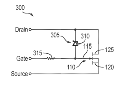
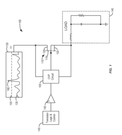
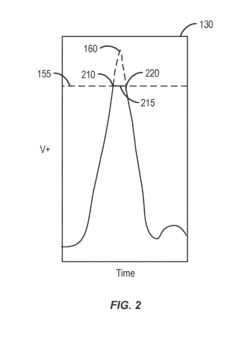
GaN OVERVOLTAGE PROTECTION CIRCUIT
PatentActiveUS20160049786A1
Innovation
- Incorporating an overvoltage protection circuit that includes a voltage sensing circuit with a diode or transistor coupled between the drain and gate terminals, which temporarily conducts to reduce resistance and prevent damage, and can activate additional protection mechanisms such as disabling gate drives and notifying control circuits.
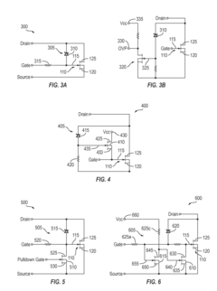
A gallium nitride (GAN) device with leakage current-based over-voltage protection
PatentWO2014031825A1
Innovation
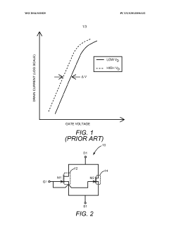
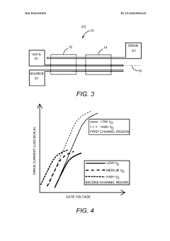
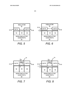
- A GaN device with a second channel region having enhanced drain-induced barrier lowering (DIBL) is designed, where the drain voltage is safely clamped below destructive levels by allowing substantial drain current to flow through this region, incorporating segmented gates and varying gate dimensions to control DIBL.
Thermal Management Strategies for GaN Under Surge Conditions
Effective thermal management is critical for GaN power devices operating under surge and transient conditions, as these events can cause rapid temperature spikes that exceed normal operating parameters. The inherent properties of GaN, including its high thermal conductivity and wide bandgap, provide some natural advantages for heat dissipation, but dedicated thermal management strategies are essential to prevent catastrophic failures during surge events.
Advanced packaging technologies represent a primary approach to thermal management for GaN devices. Direct bonded copper (DBC) substrates and advanced thermal interface materials (TIMs) with high thermal conductivity help to efficiently transfer heat away from the active device regions. Novel packaging solutions such as embedded cooling channels and integrated heat spreaders are being developed specifically for GaN applications to address the unique thermal challenges posed by surge conditions.
Active cooling systems provide another layer of protection against thermal runaway during surge events. These systems may include microfluidic cooling channels, phase-change materials, or thermoelectric coolers that can rapidly respond to temperature fluctuations. The integration of temperature sensors and feedback control mechanisms allows these systems to dynamically adjust cooling capacity based on real-time thermal conditions, providing enhanced protection during transient events.
Thermal simulation and modeling tools have become increasingly sophisticated for GaN device design. Computational fluid dynamics (CFD) and finite element analysis (FEA) enable designers to predict thermal behavior under various surge conditions, identifying potential hotspots and optimizing thermal management strategies before physical prototyping. These simulation capabilities are particularly valuable for understanding the complex thermal dynamics that occur during short-duration, high-energy surge events.
System-level thermal management approaches consider the entire power conversion system rather than just the GaN device itself. This holistic approach includes optimized PCB layouts with thermal vias, strategic component placement to minimize thermal coupling, and coordinated cooling strategies across multiple components. Some advanced designs incorporate thermal energy storage elements that can temporarily absorb heat during surge events, preventing critical temperature thresholds from being exceeded.
Emerging technologies such as diamond heat spreaders, graphene thermal interfaces, and 3D-printed cooling structures show promise for next-generation thermal management in GaN devices. These materials and structures offer unprecedented thermal conductivity and can be tailored to address the specific thermal challenges of GaN under surge conditions, potentially enabling higher power densities and improved reliability in future power electronic systems.
Standardization and Testing Protocols for GaN Reliability
The standardization and testing protocols for GaN reliability represent a critical framework for ensuring consistent evaluation and qualification of GaN power devices across the industry. Currently, the reliability assessment of GaN devices lacks unified standards specifically tailored to their unique material properties and failure mechanisms, particularly under surge and transient conditions.
Major standardization bodies including JEDEC, IEC, and AEC have begun developing specialized test methodologies for wide bandgap semiconductors. JEDEC JC-70 committee has established working groups focused on GaN reliability qualification, while IEC TC47 is adapting existing silicon-based standards to accommodate GaN's distinct characteristics. These efforts aim to address the gap between traditional silicon-based testing protocols and the requirements for GaN technology.
Key testing protocols under development include dynamic Ron characterization methods, which assess the charge trapping phenomena unique to GaN devices. These protocols typically involve stress-measure-stress sequences at various voltage levels and temperatures to capture threshold voltage shifts and on-resistance degradation patterns specific to GaN HEMTs.
Surge immunity testing represents another critical area requiring standardization. Current approaches involve subjecting devices to controlled voltage and current pulses of varying amplitudes and durations to evaluate breakdown mechanisms. However, the industry lacks consensus on pulse parameters that accurately represent real-world transient events in GaN applications.
Accelerated lifetime testing protocols are being refined to better correlate with actual field reliability. These include High Temperature Reverse Bias (HTRB), High Temperature Gate Bias (HTGB), and Temperature Humidity Bias (THB) tests modified with GaN-specific stress conditions and failure criteria. The challenge lies in determining appropriate acceleration factors that don't trigger failure modes absent in normal operation.
Thermal characterization standards are evolving to address GaN's unique thermal properties and packaging considerations. Transient thermal impedance measurements are particularly important given GaN's operation at higher frequencies and power densities compared to silicon devices.
Round-robin testing initiatives across multiple laboratories are underway to validate proposed standards and ensure reproducibility of results. These collaborative efforts aim to establish confidence in test methodologies before formal standardization, with particular focus on surge and transient testing protocols where measurement techniques remain most variable across the industry.
Unlock deeper insights with Patsnap Eureka Quick Research — get a full tech report to explore trends and direct your research. Try now!
Generate Your Research Report Instantly with AI Agent
Supercharge your innovation with Patsnap Eureka AI Agent Platform!