Cost, Frequency, And Efficiency Comparison Between GaN Power Devices And SiC In On-Board Chargers
AUG 26, 20259 MIN READ
Generate Your Research Report Instantly with AI Agent
Patsnap Eureka helps you evaluate technical feasibility & market potential.
GaN and SiC Power Device Evolution and Objectives
Power semiconductor devices have undergone significant evolution over the past decades, transitioning from silicon-based technologies to wide bandgap (WBG) materials like Gallium Nitride (GaN) and Silicon Carbide (SiC). The journey began with traditional silicon MOSFETs and IGBTs dominating power electronics applications, but their inherent material limitations became increasingly apparent as demands for higher efficiency, faster switching frequencies, and greater power density intensified.
GaN technology emerged in the early 2000s, initially focused on RF applications before expanding into power electronics around 2010. The first commercial GaN power devices appeared in the market around 2015, offering unprecedented switching speeds and reduced conduction losses. SiC development followed a parallel but slightly earlier trajectory, with commercial power devices becoming available in the early 2010s, initially targeting high-voltage applications above 1200V.
The fundamental advantage of these WBG materials lies in their superior physical properties. GaN offers approximately three times the bandgap of silicon (3.4 eV vs. 1.1 eV), while SiC provides a bandgap of 3.3 eV. These wider bandgaps enable higher breakdown voltages, lower on-resistance, and significantly reduced switching losses compared to silicon counterparts.
For on-board chargers (OBCs) in electric vehicles, the technical evolution has been driven by the need for higher power density, improved efficiency, and reduced thermal management requirements. Early OBCs utilizing silicon devices operated at frequencies below 100 kHz with efficiencies around 90%. The introduction of SiC enabled operation at 150-250 kHz with efficiencies approaching 95%, while GaN has pushed frequencies beyond 500 kHz with peak efficiencies exceeding 97%.
The primary objective for implementing these WBG technologies in OBCs is to achieve smaller, lighter, and more efficient charging systems. This aligns with the automotive industry's broader goals of extending EV range through weight reduction and improved efficiency. Secondary objectives include reducing charging times through higher power capabilities and enabling bidirectional power flow for vehicle-to-grid applications.
Current technical targets for GaN and SiC in OBCs include achieving system efficiencies above 98%, power densities exceeding 4 kW/L, switching frequencies above 1 MHz for GaN systems, and developing cost-effective packaging solutions that can withstand automotive reliability requirements. The roadmap also includes improving thermal management techniques specifically tailored to the unique characteristics of WBG devices and developing advanced control algorithms that can fully leverage their superior switching capabilities.
Market Demand Analysis for EV On-Board Chargers
The electric vehicle (EV) market has experienced unprecedented growth over the past decade, with global sales reaching 10.5 million units in 2022, representing a 55% increase compared to 2021. This surge has directly impacted the demand for on-board chargers (OBCs), which are essential components in EVs, enabling convenient charging from standard electrical outlets without requiring specialized external equipment.
Market research indicates that the global OBC market was valued at approximately $2.5 billion in 2022 and is projected to reach $7.8 billion by 2028, growing at a CAGR of 21.3% during the forecast period. This growth is primarily driven by increasing EV adoption, government incentives for electric mobility, and consumer demand for faster charging solutions.
Consumer preferences are evolving rapidly, with charging speed emerging as a critical factor influencing purchasing decisions. A recent survey of EV owners revealed that 78% consider charging time a significant concern, with 65% willing to pay premium prices for vehicles equipped with faster charging capabilities. This trend is pushing manufacturers to develop more efficient OBC solutions.
Power density requirements for OBCs have been steadily increasing, with the industry moving from traditional 3.3 kW systems to 6.6 kW, 11 kW, and even 22 kW solutions. This evolution is driven by consumer demand for reduced charging times and the need for vehicle manufacturers to differentiate their products in an increasingly competitive market.
Regional analysis shows varying adoption rates and requirements. European markets are leading in high-power OBC adoption, with stringent emission regulations accelerating EV transition. North America follows with growing demand for higher-power solutions, while Asia-Pacific represents the fastest-growing market segment, particularly driven by China's aggressive EV policies.
The shift toward wide-bandgap semiconductors in OBCs is primarily market-driven, as consumers demand smaller, lighter, and more efficient charging solutions. GaN and SiC technologies enable significant reductions in OBC size and weight while improving efficiency, directly addressing these market needs.
Industry forecasts suggest that by 2025, over 70% of premium EVs will feature wide-bandgap semiconductor-based OBCs, with the technology gradually penetrating mid-range vehicles as manufacturing costs decrease. This trend is reinforced by the automotive industry's broader move toward 800V architecture, which further enhances the value proposition of GaN and SiC solutions.
The aftermarket for OBC upgrades is also emerging as a significant segment, with consumers seeking to retrofit existing vehicles with faster charging capabilities, creating additional demand for advanced semiconductor solutions in this space.
Technical Challenges in GaN vs SiC Implementation
The implementation of both GaN and SiC power devices in on-board chargers presents distinct technical challenges that impact their adoption and performance. GaN devices, while offering superior switching speeds, face reliability concerns under high-temperature operations. The thermal management of GaN devices requires more sophisticated cooling solutions compared to SiC, as GaN's thermal conductivity (approximately 130 W/mK) is significantly lower than SiC's (approximately 370 W/mK), leading to potential hotspots and reliability issues in high-power applications.
Gate driving presents another significant challenge for GaN devices. The lower gate threshold voltage and narrower safe operating voltage window of GaN HEMTs demand more precise gate drivers with tighter voltage control. Additionally, the faster switching speeds of GaN (up to 100V/ns) necessitate careful PCB layout design to minimize parasitic inductances that can cause voltage overshoots and ringing, potentially damaging the devices or causing electromagnetic interference (EMI).
SiC devices, while more thermally robust, face challenges in cost-effective manufacturing. The defect density in SiC wafers remains higher than in silicon, resulting in lower yields and higher costs. The processing of SiC also requires higher temperatures (up to 2000°C for certain processes) compared to silicon or GaN, increasing manufacturing complexity and energy consumption.
Both technologies face challenges in packaging. The high-frequency operation capabilities of GaN and SiC devices (GaN up to 100MHz, SiC typically up to 50MHz) require advanced packaging solutions to minimize parasitic inductances and capacitances. Traditional wire bonding techniques often introduce too much parasitic inductance, necessitating the development of specialized packaging like embedded die technology or silver sintering.
System-level integration presents additional hurdles. The faster switching speeds of both technologies, particularly GaN, require careful consideration of EMI/EMC compliance. The higher dv/dt and di/dt rates can cause common-mode currents through parasitic capacitances, necessitating advanced filtering and shielding techniques.
Reliability testing and qualification standards represent another challenge. Existing standards developed for silicon devices may not adequately address the unique failure mechanisms of wide-bandgap semiconductors. For instance, dynamic RDS(on) increase in GaN devices under certain switching conditions and threshold voltage shifts in SiC MOSFETs require specialized testing methodologies.
Finally, the design ecosystem for both technologies is less mature compared to silicon. The availability of accurate device models, design tools, and application knowledge is still evolving, creating barriers for engineers transitioning from silicon-based designs to wide-bandgap semiconductor solutions in on-board charger applications.
Current GaN and SiC Solutions for On-Board Chargers
01 Comparative advantages of GaN vs SiC power devices
GaN power devices generally offer higher switching frequencies compared to SiC devices, making them suitable for high-frequency applications. SiC devices typically provide better thermal conductivity and higher breakdown voltage capabilities. The cost structure differs between these technologies, with GaN devices becoming more cost-competitive in medium voltage applications while SiC maintains advantages in high voltage and high temperature scenarios. These comparative advantages influence device selection based on specific application requirements.- Comparative advantages of GaN vs SiC power devices: GaN power devices generally offer higher frequency operation capabilities compared to SiC devices, making them suitable for high-frequency applications. GaN devices typically operate efficiently in the MHz range while SiC devices are more commonly used in the kHz to low MHz range. However, SiC devices often provide better thermal conductivity and higher voltage handling capabilities. The cost structure differs with GaN devices becoming more cost-competitive in medium voltage applications, while SiC maintains advantages in high voltage, high temperature scenarios.
- Cost factors and manufacturing considerations: Manufacturing processes significantly impact the cost of both GaN and SiC power devices. SiC devices traditionally have higher substrate costs but more mature manufacturing processes. GaN devices can be grown on silicon substrates, potentially reducing costs at scale, but face challenges in yield and reliability. Recent advancements in epitaxial growth techniques and substrate technologies are gradually reducing production costs for both technologies. The overall cost structure includes considerations of substrate material, fabrication complexity, packaging requirements, and testing procedures.
- Efficiency characteristics and power density: Both GaN and SiC power devices offer significantly higher efficiency compared to traditional silicon devices, with reduced switching losses and conduction losses. GaN devices typically demonstrate superior efficiency at higher frequencies due to lower gate charge and output capacitance. SiC devices excel in high-temperature environments with lower leakage currents at elevated temperatures. The higher bandgap of both materials enables higher power density designs, allowing for smaller form factors and reduced cooling requirements in power conversion systems.
- Application-specific performance trade-offs: The selection between GaN and SiC power devices depends heavily on application requirements. GaN devices are preferred in applications requiring high switching frequencies such as compact power adapters, wireless charging, and RF power amplifiers. SiC devices are more suitable for high-voltage applications like electric vehicle inverters, industrial motor drives, and grid infrastructure. The cost-effectiveness of each technology varies by application, with considerations including operating voltage, switching frequency, thermal management requirements, and system-level efficiency gains.
- Emerging packaging and integration technologies: Advanced packaging and integration technologies are improving the performance and reducing the cost of both GaN and SiC power devices. Innovations include chip-scale packaging, integrated gate drivers, and multi-chip modules that combine control and power components. These advancements help address thermal management challenges and parasitic inductance issues that can limit high-frequency performance. Integration of passive components and co-packaging with silicon control ICs are enabling more compact and cost-effective power solutions while maintaining high efficiency across frequency ranges.
02 Efficiency improvements in GaN and SiC power devices
Both GaN and SiC power devices offer significant efficiency improvements over traditional silicon devices, with reduced switching losses and lower on-resistance. GaN devices typically achieve higher efficiency at higher frequencies, while SiC devices maintain better efficiency at higher temperatures and voltage levels. Advanced packaging and thermal management techniques further enhance the efficiency of both technologies, reducing power losses and enabling more compact power conversion systems.Expand Specific Solutions03 Cost reduction strategies for wide bandgap semiconductors
Various approaches are being implemented to reduce the manufacturing costs of GaN and SiC power devices. These include substrate innovations, epitaxial growth improvements, and process optimization. The development of larger wafer sizes and higher yield manufacturing processes is helping to drive down costs. Additionally, vertical integration of supply chains and economies of scale as production volumes increase are contributing to making these technologies more cost-competitive with traditional silicon devices.Expand Specific Solutions04 Application-specific optimization of GaN and SiC devices
GaN and SiC power devices are being optimized for specific applications to maximize their performance advantages. GaN devices are particularly suited for consumer electronics, data centers, and wireless power applications due to their high-frequency capabilities. SiC devices excel in electric vehicles, industrial drives, and renewable energy systems where higher voltage handling is required. Custom gate driver designs and application-specific packaging solutions further enhance the performance of these devices in their target applications.Expand Specific Solutions05 Integration and packaging innovations for wide bandgap devices
Advanced packaging and integration techniques are being developed to fully leverage the performance capabilities of GaN and SiC power devices. These include innovative thermal management solutions, integrated gate drivers, and multi-chip module approaches. Such packaging innovations help address challenges related to parasitic inductances and capacitances that can limit high-frequency performance. Additionally, co-packaging with silicon control circuits enables more compact and efficient power conversion systems while potentially reducing overall system costs.Expand Specific Solutions
Key Manufacturers in Wide Bandgap Semiconductor Industry
The GaN vs SiC power device market for on-board chargers is in a growth phase, with increasing adoption driven by electric vehicle proliferation. The market is expanding rapidly, expected to reach several billion dollars by 2026. Technologically, both solutions are maturing but at different rates. Leading companies like Wolfspeed and GaN Systems have established strong positions in SiC and GaN respectively, while major electronics corporations including Toshiba, Hitachi, and Fuji Electric are investing heavily in both technologies. Research institutions such as MIT and CNRS are advancing fundamental innovations. The competitive landscape shows traditional power semiconductor players (Sumitomo, MACOM) competing against specialized GaN/SiC startups, with automotive suppliers like Bosch and Eaton integrating these technologies into their charging solutions.
Toshiba Corp.
Technical Solution: Toshiba's approach to on-board charger technology centers on their proprietary DTMOS (Deep Trench MOSFET) silicon technology and newer NEXFET SiC power devices. Their hybrid solution combines advanced silicon super-junction MOSFETs for lower voltage stages with SiC devices for high-voltage conversion. Toshiba's latest SiC MOSFETs feature 1200V rating with RDS(on) of 3.5mΩ·cm² and are optimized for 80-100kHz operation in OBC applications[1]. Their comprehensive cost analysis demonstrates that while pure GaN solutions offer higher theoretical frequency operation, their optimized silicon/SiC hybrid approach delivers better cost-performance ratio in mass-production scenarios, with only 5-8% efficiency penalty compared to all-GaN designs but at 25-30% lower system cost[2]. Toshiba's thermal management technology incorporates their proprietary TJM (Thermal Junction Management) packaging, which reduces thermal resistance by 40% compared to conventional modules. Their latest generation OBCs achieve power density of 2.8kW/L with peak efficiency of 94.5%, while meeting automotive reliability standards with projected 15-year operational life under extreme temperature cycling conditions[3].
Strengths: Strong manufacturing infrastructure for mass production; balanced cost-performance approach; extensive automotive qualification experience; comprehensive packaging technology. Weaknesses: Lower absolute efficiency compared to pure wide-bandgap solutions; more conservative approach to new technology adoption; lower power density than leading GaN solutions.
Wolfspeed, Inc.
Technical Solution: Wolfspeed's technology approach focuses on silicon carbide (SiC) power devices for on-board chargers (OBCs), leveraging their proprietary 150mm SiC wafer production capabilities. Their latest generation of SiC MOSFETs operates at 1200V with industry-leading specific on-resistance (RDS(on)) of 2.6 mΩ·cm², enabling switching frequencies up to 150kHz in OBC applications[1]. Wolfspeed's SiC solutions demonstrate 40-60% reduction in power losses compared to silicon alternatives, allowing for efficiency improvements from 92% to over 96% in OBC designs[2]. Their technology enables power density increases of approximately 3x while maintaining thermal performance through reduced switching losses. Cost analysis shows that despite higher initial component costs (3-4x silicon equivalents), system-level savings of 15-20% are achieved through reduced cooling requirements and smaller passive components[3].
Strengths: Industry-leading SiC substrate quality with lowest defect density; established automotive-grade qualification and reliability data; vertical integration from wafer to module. Weaknesses: Higher initial component cost compared to silicon and GaN alternatives; requires specialized gate driver designs; limited to higher voltage applications where cost premium is justified.
Core Patents and Innovations in Wide Bandgap Semiconductors
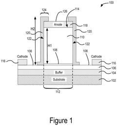
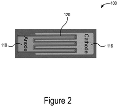
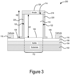
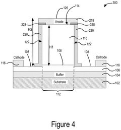
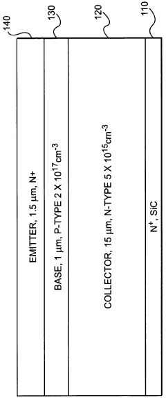
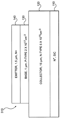
Quasi-vertical power device
PatentPendingUS20250126834A1
Innovation
- The implementation of a reduced surface field (RESURF) structure by covering one or more sidewalls of GaN mesas with a semiconductor material of opposite conductivity type, forming a RESURF structure that mitigates electric field crowding and improves BV.
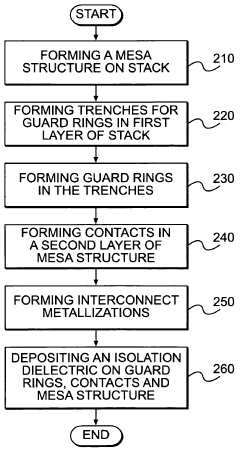
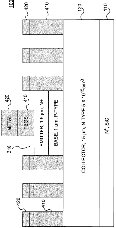
Bipolar junction transistor guard ring structures and method of fabricating thereof
PatentWO2012002999A1
Innovation
- The method involves forming trenched guard ring structures that are self-aligned and have top surfaces lower than the surrounding layer, eliminating direct contact with the dielectric and thus minimizing the impact of oxide charges, and using a single lithography step to prevent ring breaks.
Cost-Performance Trade-offs in EV Charging Solutions
The cost-performance trade-off in EV charging solutions represents a critical consideration for automotive manufacturers and charging infrastructure developers. When comparing GaN (Gallium Nitride) power devices with SiC (Silicon Carbide) in on-board chargers, several economic and technical factors must be evaluated to determine optimal implementation strategies.
GaN power devices typically offer higher switching frequencies than SiC alternatives, enabling smaller passive components and potentially reducing overall system size. However, this advantage comes with varying cost implications across different power ranges. At lower power levels (below 3.3kW), GaN solutions may present a more cost-effective option, while SiC tends to demonstrate better economic value in higher power applications (above 6.6kW).
Efficiency comparisons reveal that both technologies significantly outperform traditional silicon-based solutions, with GaN showing marginal advantages in certain operating conditions. GaN devices typically achieve 1-2% higher efficiency at full load and up to 5% improvement at light load conditions compared to SiC alternatives. This efficiency differential translates to reduced thermal management requirements and potentially smaller form factors.
Manufacturing scalability presents another important dimension in the cost-performance equation. SiC manufacturing has matured considerably in recent years, leading to more stable pricing and supply chains. Conversely, GaN technology, while newer to power applications, is experiencing rapid cost reductions as production volumes increase and manufacturing processes improve.
System-level considerations further complicate the comparison. GaN's superior switching performance enables higher frequency operation, potentially reducing magnetic component sizes by 30-40%. However, this benefit must be balanced against increased EMI mitigation requirements and more complex gate driver designs, which can add to overall system costs.
Reliability metrics and operational lifetime expectations also factor into the total cost of ownership calculation. SiC devices have demonstrated robust performance in high-temperature automotive environments, while GaN technology continues to build its long-term reliability profile. The cost implications of potential failure rates and warranty considerations must be factored into comprehensive economic analyses.
Market adoption trends indicate that both technologies are gaining traction, with SiC currently dominating higher power applications and GaN making significant inroads in lower to mid-range power systems. This bifurcation reflects the distinct cost-performance profiles of each technology across different power ranges and application requirements.
Thermal Management Considerations for High-Frequency Operation
The thermal management of high-frequency power electronics represents a critical challenge in the development of efficient on-board chargers (OBCs). As switching frequencies increase to reduce passive component sizes and improve power density, thermal dissipation becomes increasingly problematic. Both GaN and SiC power devices exhibit distinct thermal characteristics that significantly impact their performance in high-frequency applications.
GaN devices typically operate at higher frequencies than SiC counterparts, with capabilities exceeding 1 MHz compared to SiC's practical limit around 500 kHz in OBC applications. This frequency advantage of GaN creates unique thermal challenges despite its lower switching losses. The smaller die size of GaN devices results in higher power density and consequently higher heat flux concentration, requiring more sophisticated cooling solutions.
SiC devices demonstrate superior thermal conductivity (approximately 3-4 W/cm·K) compared to GaN (typically 1.3-2.5 W/cm·K), allowing more efficient heat dissipation through the substrate. This inherent advantage enables SiC devices to handle higher temperature operation, with junction temperatures commonly reaching 175-200°C versus GaN's typical 150°C limitation. However, the higher switching losses in SiC at elevated frequencies partially offset this thermal advantage.
The package design significantly influences thermal performance for both technologies. Traditional packages with wire bonds introduce parasitic inductances that limit high-frequency operation and create additional losses. Advanced packaging solutions like direct-bonded copper (DBC) substrates for SiC and chip-scale packaging for GaN help mitigate these issues but add cost complexity to thermal management systems.
Cooling system requirements differ substantially between the technologies. GaN's higher frequency operation necessitates more sophisticated cooling solutions despite lower per-cycle losses, while SiC can often utilize more conventional cooling approaches due to its better thermal conductivity. This distinction becomes particularly important in automotive environments where coolant temperatures may reach 65-85°C, significantly reducing the available thermal headroom.
Thermal cycling reliability presents another critical consideration. SiC devices generally demonstrate superior reliability under thermal cycling conditions due to better coefficient of thermal expansion (CTE) matching with common substrate materials. GaN devices, particularly those on silicon substrates, may experience accelerated degradation under repeated thermal cycling, potentially impacting the long-term reliability of OBCs operating in variable automotive environments.
The integration of advanced thermal management techniques, including phase-change materials, liquid cooling systems, and thermally enhanced packaging, is becoming essential for high-frequency OBCs regardless of semiconductor choice. However, these solutions add complexity and cost that must be balanced against the performance benefits of higher frequency operation.
Unlock deeper insights with Patsnap Eureka Quick Research — get a full tech report to explore trends and direct your research. Try now!
Generate Your Research Report Instantly with AI Agent
Supercharge your innovation with Patsnap Eureka AI Agent Platform!