

PCB Layout Blueprint For GaN Power Devices: Loop Inductance And Return Paths
AUG 26, 202510 MIN READ
Generate Your Research Report Instantly with AI Agent
PatSnap Eureka helps you evaluate technical feasibility & market potential.
GaN Power Device PCB Layout Evolution and Objectives
Gallium Nitride (GaN) power devices have revolutionized power electronics since their commercial introduction in the early 2010s. The evolution of PCB layout techniques for these devices has been driven by their unique characteristics: faster switching speeds, higher power density, and lower on-resistance compared to traditional silicon-based MOSFETs. This technological progression has necessitated fundamental changes in PCB design philosophy to fully leverage GaN's capabilities while mitigating its inherent challenges.
The historical development of GaN power device PCB layouts can be traced through three distinct phases. Initially (2010-2015), designs primarily focused on adapting existing silicon-based layouts with minimal modifications, resulting in suboptimal performance as the unique properties of GaN were not fully accommodated. The second phase (2015-2020) saw the emergence of GaN-specific design principles, particularly emphasizing loop inductance reduction and proper thermal management. The current phase (2020-present) represents a mature understanding of GaN requirements, with sophisticated multi-layer designs that optimize both electrical and thermal performance.
Loop inductance has emerged as a critical factor in GaN PCB layouts due to the extremely fast switching speeds (up to 200V/ns) these devices can achieve. Even small parasitic inductances can generate significant voltage spikes during switching transitions, potentially damaging components and increasing electromagnetic interference (EMI). This has driven the evolution from traditional loop layouts to advanced techniques like vertical power loops and embedded power planes.
Return path optimization has similarly evolved from an afterthought to a primary design consideration. Early GaN implementations often suffered from ground bounce and common-mode noise issues due to improper return path planning. Modern designs now incorporate dedicated return path layers and strategic via placement to minimize impedance discontinuities.
The primary objectives of contemporary GaN PCB layout techniques center around four key areas: minimizing loop inductance to enable faster switching without voltage overshoots; optimizing thermal management to handle GaN's high power density; reducing EMI through controlled impedance and proper shielding; and ensuring long-term reliability under high-frequency, high-power operation.
Looking forward, the industry aims to standardize GaN-specific PCB design methodologies while pushing the boundaries of integration density. Emerging objectives include the development of automated design tools specifically calibrated for GaN characteristics, implementation of embedded cooling solutions directly within PCB structures, and creation of modular design approaches that can accelerate time-to-market for GaN-based power systems.
Market Demand Analysis for High-Frequency GaN Applications
The global market for GaN power devices is experiencing unprecedented growth, driven primarily by the increasing demand for high-frequency applications across multiple industries. Current market research indicates that the GaN power device market is projected to grow at a CAGR of 22.9% from 2021 to 2026, reaching a value of $1.8 billion by the end of the forecast period. This remarkable growth trajectory is underpinned by the superior performance characteristics of GaN technology compared to traditional silicon-based solutions.
The automotive sector represents one of the most significant market opportunities for high-frequency GaN applications. With electric vehicles (EVs) gaining mainstream adoption, the demand for efficient power conversion systems has intensified. GaN-based onboard chargers and DC-DC converters offer substantial advantages in terms of size reduction and efficiency improvement, which directly translates to extended driving range and faster charging capabilities for EVs.
Telecommunications infrastructure, particularly with the global rollout of 5G networks, constitutes another major market driver. The higher frequency capabilities of GaN RF devices make them ideal for 5G base stations, where they deliver improved power efficiency and bandwidth compared to legacy technologies. Industry analysts estimate that GaN penetration in telecom infrastructure could reach 35% by 2025, representing a substantial market opportunity.
Consumer electronics manufacturers are increasingly adopting GaN technology for fast-charging solutions. The compact size and thermal efficiency of GaN-based chargers have created a rapidly expanding market segment, with major smartphone manufacturers now shipping GaN chargers with premium devices. This consumer-facing application has significantly raised awareness of GaN technology benefits among end-users.
Data center power infrastructure represents an emerging high-value market for GaN technology. With data centers consuming approximately 1% of global electricity and facing increasing pressure to improve efficiency, GaN-based power supplies offer compelling advantages. The reduced switching losses and higher operating frequencies enable more compact and efficient power delivery architectures, addressing critical challenges in modern data center design.
Industrial power conversion systems are gradually transitioning to GaN technology, driven by efficiency regulations and operational cost considerations. Applications include motor drives, renewable energy inverters, and industrial power supplies, where the benefits of reduced switching losses and higher power density deliver tangible economic advantages.
The market demand for optimized PCB layouts specifically designed for GaN power devices is growing in parallel with device adoption. Engineering teams increasingly recognize that realizing the full performance potential of GaN technology requires specialized layout techniques that minimize loop inductance and optimize return paths. This has created a secondary market for design expertise, specialized CAD tools, and reference designs focused on high-frequency GaN applications.
Current Challenges in GaN PCB Layout Design
Despite the significant advantages of Gallium Nitride (GaN) power devices, including higher switching speeds and improved efficiency, PCB layout design for these components presents several formidable challenges. The primary obstacle stems from GaN's inherent high-speed switching capability (typically 100-200 V/ns), which makes parasitic inductances in PCB layouts particularly problematic. Even minimal loop inductances of 1-2 nH can generate substantial voltage spikes exceeding 200V during switching transitions, potentially damaging devices and creating electromagnetic interference (EMI).
Traditional PCB layout methodologies developed for silicon-based devices prove inadequate for GaN applications. The conventional two-layer board designs with separated power and ground planes introduce excessive loop areas, creating unacceptable parasitic inductances. Additionally, standard FR-4 PCB materials exhibit dielectric losses that become significant at the high frequencies where GaN devices operate most efficiently.
Thermal management presents another critical challenge. GaN devices generate concentrated heat during operation, requiring sophisticated thermal dissipation strategies within the PCB design. The compact packaging of GaN components further complicates this issue, as designers must balance electrical performance with thermal considerations in increasingly dense layouts.
Signal integrity issues are magnified in GaN applications due to the extremely fast rise and fall times. Gate drive circuits are particularly susceptible to noise coupling and ground bounce effects, which can lead to false triggering or shoot-through conditions. The gate drive loop must be carefully designed with minimal inductance while maintaining isolation from power switching noise.
Return path discontinuities represent a significant design challenge specific to GaN implementations. When high-frequency current encounters a discontinuity in its return path, it creates electromagnetic fields that couple to adjacent circuits, generating noise and potential instability. Designers must ensure continuous, low-impedance return paths directly beneath signal traces to minimize this effect.
Component placement constraints further complicate GaN PCB layouts. Critical components like decoupling capacitors must be positioned extremely close to power devices to minimize loop inductance, often requiring specialized mounting techniques or custom footprints. The physical limitations of component sizes and clearance requirements create significant design trade-offs.
Measurement and validation of GaN-based designs present additional challenges. Traditional oscilloscope probes and measurement techniques can introduce loading effects that distort the very parameters being measured. Specialized high-bandwidth probes with minimal ground leads are required, along with careful measurement methodologies that account for probe-induced effects.
These challenges collectively necessitate a fundamental rethinking of PCB layout approaches for GaN power applications, with particular emphasis on minimizing loop inductances and optimizing return paths through advanced multi-layer designs, embedded components, and specialized materials.
Current PCB Layout Methodologies for Loop Inductance Minimization
01 PCB layout techniques to minimize loop inductance
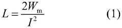
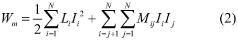
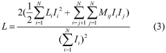
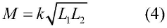
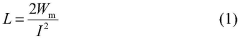
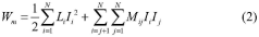
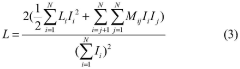
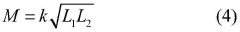
Specific PCB layout techniques can significantly reduce loop inductance in GaN power device circuits. These include optimizing trace routing, minimizing the distance between components, using ground planes effectively, and implementing symmetrical layouts. Proper component placement and orientation are crucial for reducing parasitic inductance in high-frequency switching applications, which helps improve switching performance and reduce electromagnetic interference.- PCB layout techniques to minimize loop inductance: Specific PCB layout techniques can significantly reduce loop inductance in GaN power device circuits. These include optimizing trace routing with shorter, wider paths, using ground planes directly beneath signal traces, and implementing symmetrical layouts. Minimizing the physical loop area between gate drivers and GaN devices is critical, as is careful placement of decoupling capacitors as close as possible to the power devices to reduce parasitic inductance in the power loop.
- Multi-layer PCB designs for GaN power applications: Multi-layer PCB designs offer significant advantages for reducing loop inductance in GaN power circuits. By utilizing multiple layers with strategic via placement, designers can create three-dimensional current paths that minimize loop areas. Power and ground planes on adjacent layers create low-inductance paths, while dedicated layers for gate drive circuits help isolate sensitive control signals from power switching noise. These designs often incorporate embedded capacitance between layers to further reduce high-frequency impedance.
- Advanced packaging and interconnect solutions: Advanced packaging technologies help minimize loop inductance in GaN power circuits. These include flip-chip mounting, embedded die technology, and specialized interconnect structures that reduce connection lengths. Some designs incorporate co-packaged gate drivers with GaN devices to minimize critical loop areas. Innovative substrate materials with optimized thermal and electrical properties support higher power density while maintaining low inductance paths. These packaging solutions often integrate multiple components into a single module to minimize interconnection distances.
- Simulation and modeling techniques for loop inductance optimization: Electromagnetic simulation and modeling tools are essential for optimizing GaN power circuit layouts to minimize loop inductance. These tools enable accurate prediction of parasitic inductances before physical implementation, allowing designers to evaluate multiple layout options. Advanced 3D field solvers can identify hotspots of high inductance, while specialized extraction tools quantify parasitic elements in complex layouts. Time-domain simulations help assess switching behavior under realistic conditions, enabling designers to balance trade-offs between inductance, thermal performance, and EMI considerations.
- Novel power loop structures and topologies: Innovative power loop structures and circuit topologies can fundamentally reduce loop inductance in GaN power applications. These include vertical power loop designs that minimize the physical loop area in three dimensions, interleaved power stage arrangements that reduce effective loop inductance through parallel paths, and integrated current sensing methods that don't add inductance to critical paths. Some designs incorporate resonant switching techniques that are less sensitive to loop inductance, while others use specialized magnetic components to counteract the effects of unavoidable parasitic inductance.
02 Multi-layer PCB designs for GaN power devices
Multi-layer PCB designs offer significant advantages for reducing loop inductance in GaN power circuits. By utilizing multiple layers with strategic via placement, power and ground planes can be positioned closer together, creating lower impedance paths. These designs enable shorter current return paths and allow for better thermal management, which is critical for high-power GaN applications where switching speeds and power density are high.Expand Specific Solutions03 Integrated packaging solutions for GaN devices
Advanced packaging technologies integrate GaN devices with optimized interconnects to minimize loop inductance. These solutions include embedding passive components within the package, using flip-chip mounting techniques, and implementing advanced substrate materials. Such integrated approaches reduce the physical distance between components and provide better control over parasitic elements, resulting in improved switching performance and higher power efficiency.Expand Specific Solutions04 Gate driver placement and routing optimization
The placement and routing of gate drivers relative to GaN power devices significantly impacts loop inductance. Optimal positioning involves placing gate drivers as close as possible to the GaN devices, using dedicated power and ground planes for gate drive circuits, and implementing Kelvin connections. These techniques minimize gate loop inductance, which is critical for controlling switching speeds and preventing parasitic oscillations in high-frequency GaN applications.Expand Specific Solutions05 Thermal management integrated with inductance reduction
Advanced PCB designs for GaN power devices simultaneously address thermal management and loop inductance reduction. These approaches include using thermal vias, copper coins, and specialized substrate materials that provide both electrical and thermal benefits. By integrating cooling solutions directly into the PCB design while maintaining low-inductance layouts, these techniques enable GaN devices to operate at higher power densities without compromising switching performance or reliability.Expand Specific Solutions
Leading Manufacturers and Design Houses in GaN Technology
The GaN power device PCB layout market is currently in a growth phase, characterized by increasing adoption across automotive, consumer electronics, and renewable energy sectors. The market is expanding rapidly with a projected CAGR of 15-20% over the next five years, driven by demand for higher efficiency power conversion solutions. Leading companies like GaN Systems and Efficient Power Conversion Corp. have established strong technical foundations in loop inductance optimization and return path design, while newer entrants such as Cambridge GaN Devices and InnoScience are gaining momentum through innovative approaches. Academic institutions including Xidian University and University of Electronic Science & Technology of China are contributing significant research advancements. The technology is approaching maturity in certain applications, though challenges in thermal management and high-frequency layout techniques remain areas for competitive differentiation among market players.
GaN Systems, Inc.
Technical Solution: GaN Systems has developed a comprehensive PCB layout blueprint specifically for GaN power devices that focuses on minimizing loop inductance and optimizing return paths. Their approach includes a patented island technology that places the GaN transistor on an electrically isolated copper pad, creating shorter current loops and reducing parasitic inductance. The company's design methodology emphasizes symmetrical layouts with power loops kept as small as possible, typically under 10mm in length, which has been shown to reduce loop inductance by up to 60% compared to conventional designs. GaN Systems also implements advanced thermal management techniques integrated with their loop inductance reduction strategies, using copper coins and multiple vias to simultaneously address thermal concerns while maintaining optimal electrical performance. Their PCB layout guidelines specifically recommend keeping high-frequency current paths on a single layer whenever possible and using ground planes strategically to provide low-impedance return paths.
Strengths: Industry-leading expertise specifically in GaN power applications with proven designs that achieve significantly lower switching losses and EMI. Their island technology provides a unique advantage in minimizing loop inductance while maintaining thermal performance. Weaknesses: Their solutions may require more complex manufacturing processes and potentially higher production costs compared to traditional silicon-based designs.
Cambridge GaN Devices Ltd.
Technical Solution: Cambridge GaN Devices (CGD) has pioneered an innovative PCB layout approach for GaN power devices that addresses loop inductance and return path challenges through their proprietary ICeGaN™ technology. Their solution integrates gate drive and protection circuitry directly within the GaN IC, which significantly reduces the gate loop inductance - a critical factor in high-frequency switching applications. CGD's layout methodology employs a multi-layer PCB design with dedicated power and ground planes that create controlled impedance paths and minimize common-mode noise. Their designs feature strategically placed decoupling capacitors as close as possible to the GaN devices, typically within 2-3mm, which has been demonstrated to reduce switching losses by up to 30% compared to conventional placement techniques. The company has developed specific guidelines for Kelvin source connections that separate power and signal grounds to prevent noise coupling, while their return path optimization includes interdigitated power and ground traces to minimize loop areas.
Strengths: Their integrated ICeGaN™ technology provides built-in protection features while simultaneously addressing loop inductance issues, making their solutions more robust and easier to implement. Weaknesses: Their highly integrated approach may limit design flexibility for specialized applications and could potentially increase per-unit costs for lower power applications.
Critical Patents and Research on GaN Return Path Optimization
Vertical embedded capacitor PCB layout structure for reducing parasitic inductance of GaN device
PatentPendingCN117119683A
Innovation
- Using a vertically embedded capacitor PCB layout structure, GaN devices are placed on both sides of the printed circuit board and the decoupling capacitors are vertically embedded to form a high efficiency loop, reduce the power loop area, and thereby reduce parasitic inductance.
Horizontal embedded capacitor PCB layout structure for reducing parasitic inductance of GaN device
PatentActiveCN117202500A
Innovation
- Using a horizontally embedded capacitor PCB layout structure, GaN devices are arranged side by side on the printed circuit board, and decoupling capacitors are embedded horizontally to form a power loop, reducing the power loop area to reduce parasitic inductance.
Thermal Management Considerations for GaN PCB Designs
Thermal management is a critical aspect of GaN power device PCB design due to the high power density and switching speeds these devices operate at. The superior thermal conductivity of GaN compared to silicon allows for higher operating temperatures, but this advantage must be properly leveraged through effective PCB thermal design strategies.
The primary thermal challenge in GaN PCB layouts stems from the concentrated heat generation in small die areas. Unlike traditional silicon devices, GaN components can generate significant heat in extremely localized regions, creating thermal hotspots that require specialized cooling solutions. This is particularly relevant when considering the relationship between thermal management and loop inductance optimization.
Effective thermal management begins with proper component placement. Heat-generating GaN devices should be positioned to allow optimal heat dissipation while maintaining the short current loops essential for minimizing inductance. This often requires a balance between thermal and electrical performance considerations, as the ideal placement for thermal management may conflict with optimal return path design.
Thermal vias play a crucial role in GaN PCB designs, serving as conduits for heat transfer from the device layer to inner copper planes or the bottom layer. These vias should be strategically placed directly beneath GaN devices and in surrounding areas to create efficient thermal pathways. The quantity, diameter, and arrangement of thermal vias significantly impact the overall thermal resistance of the PCB structure.
Copper pour techniques must be carefully implemented to enhance thermal dissipation while maintaining proper return paths. Solid copper planes not only serve as excellent thermal conductors but also provide low-impedance return paths that reduce loop inductance. Multi-layer designs with dedicated thermal planes can effectively separate thermal management functions from signal integrity concerns.
Advanced cooling solutions such as integrated heat sinks, thermal interface materials, and active cooling mechanisms may be necessary for high-power GaN applications. These solutions must be considered early in the PCB layout process to ensure compatibility with the electrical design requirements, particularly the critical loop inductance parameters.
Thermal simulation tools have become essential for predicting hotspots and optimizing thermal management strategies in GaN PCB designs. These tools allow designers to evaluate various layout options and cooling solutions before physical prototyping, ensuring that thermal considerations do not compromise the electrical performance advantages of GaN technology.
The interdependence between thermal management and return path design creates a complex optimization challenge that requires holistic design approaches. Techniques that address both concerns simultaneously, such as segmented power planes with thermal relief connections, represent the cutting edge of GaN PCB design methodology.
EMI/EMC Compliance Strategies for GaN Power Circuits
Electromagnetic Interference (EMI) and Electromagnetic Compatibility (EMC) compliance represent critical challenges in GaN power circuit design due to the high switching speeds and steep voltage transitions inherent to GaN technology. These characteristics, while beneficial for efficiency, create significant EMI concerns that must be addressed through comprehensive design strategies.
The primary EMI/EMC compliance approach begins with proper PCB layout techniques that minimize loop inductance. By implementing optimal return path designs with minimal impedance, designers can significantly reduce radiated emissions. Strategic placement of decoupling capacitors as close as possible to GaN devices helps manage high-frequency noise components, while ground planes should be continuous and uninterrupted to provide low-impedance return paths.
Shielding techniques represent another essential compliance strategy. Proper shield design must account for the higher frequencies associated with GaN switching transitions. Effective shields require careful consideration of aperture sizes and locations to prevent unintended radiation through shield openings. In many applications, compartmentalization of circuit sections with dedicated shields provides superior EMI containment.
Filter design for GaN applications demands special attention to high-frequency performance. Common mode chokes must maintain effectiveness at the higher harmonic frequencies generated by GaN devices. Differential mode filters require careful placement to minimize parasitic effects that could compromise their performance. The integration of these filtering elements must be considered early in the design process rather than as an afterthought.
Spread spectrum techniques offer additional compliance advantages by distributing energy across frequency bands rather than concentrating it at specific frequencies. This approach can be particularly effective for meeting regulatory requirements without sacrificing system performance. Implementation typically involves modulating the switching frequency with a controlled profile to spread harmonic content.
Thermal management strategies also impact EMI/EMC compliance, as temperature variations can affect GaN device switching characteristics. Maintaining consistent thermal conditions helps ensure predictable EMI profiles throughout operation. Advanced cooling solutions that minimize thermal gradients across the PCB contribute to more stable EMI performance.
Testing methodologies for GaN-based systems require updates to traditional approaches. Near-field scanning at higher frequencies becomes essential for identifying EMI hotspots. Pre-compliance testing should incorporate higher frequency ranges than typically used for silicon-based designs. Automated test procedures that capture transient EMI events provide more comprehensive compliance verification.
Regulatory considerations continue to evolve as GaN technology becomes more prevalent. Designers must stay informed about emerging standards that may impose stricter limits on higher frequency emissions where GaN devices generate significant energy. Proactive engagement with regulatory bodies can help shape realistic compliance frameworks for this advancing technology.
Unlock deeper insights with PatSnap Eureka Quick Research — get a full tech report to explore trends and direct your research. Try now!
Generate Your Research Report Instantly with AI Agent
Supercharge your innovation with PatSnap Eureka AI Agent Platform!