Analysing the Market Adoption of Boron Nitride Nanosheets in Computing
OCT 10, 202510 MIN READ
Generate Your Research Report Instantly with AI Agent
Patsnap Eureka helps you evaluate technical feasibility & market potential.
Boron Nitride Nanosheets Background and Computing Applications
Boron Nitride Nanosheets (BNNSs) represent a significant advancement in two-dimensional (2D) materials science, emerging as a promising alternative to graphene due to their unique properties. First isolated in 2005, these atomically thin sheets consist of hexagonal arrangements of boron and nitrogen atoms, creating a structure analogous to graphene but with distinct electronic characteristics. Unlike graphene's zero bandgap, BNNSs feature a wide bandgap of approximately 5.9 eV, classifying them as excellent insulators with remarkable thermal conductivity.
The evolution of BNNSs has been marked by significant milestones in synthesis techniques. Early production methods relied on mechanical exfoliation, similar to graphene extraction, but yielded limited quantities. Recent advancements in chemical vapor deposition (CVD) and liquid-phase exfoliation have dramatically improved scalability, enabling industrial-level production while maintaining structural integrity and performance characteristics.
In computing applications, BNNSs offer transformative potential across multiple domains. Their exceptional thermal conductivity (up to 2000 W/mK) positions them as ideal candidates for thermal management in high-performance computing systems, where heat dissipation represents a critical challenge. As processor densities continue to increase following Moore's Law, conventional cooling solutions prove increasingly inadequate, creating an urgent need for materials like BNNSs that can efficiently transfer heat away from sensitive electronic components.
Beyond thermal management, BNNSs serve as excellent dielectric substrates for next-generation electronic devices. Their atomically smooth surfaces, chemical stability, and minimal electron-phonon coupling create an ideal environment for supporting other 2D materials in heterostructure configurations. This property is particularly valuable in developing ultra-thin, high-performance transistors and memory devices that can overcome the physical limitations of silicon-based technologies.
The integration of BNNSs into quantum computing architectures represents another promising frontier. Their ability to host and preserve quantum states with minimal decoherence makes them potential platforms for quantum bits (qubits). Research indicates that defects in BNNSs could function as single-photon emitters, essential components for quantum information processing and secure communications systems.
Recent technological trends indicate growing interest in BNNS-based neuromorphic computing elements. The material's unique electronic properties can be leveraged to create artificial synapses and neurons that mimic biological neural networks, potentially enabling more energy-efficient artificial intelligence systems that overcome the von Neumann bottleneck plaguing conventional computing architectures.
As computing paradigms evolve toward greater energy efficiency and performance density, BNNSs stand at the technological frontier, offering solutions to fundamental challenges in thermal management, electronic isolation, and next-generation computing architectures.
Market Demand Analysis for BN Nanosheets in Computing Industry
The computing industry's demand for advanced materials with superior thermal and electrical properties has been steadily increasing, with boron nitride nanosheets (BNNS) emerging as a promising candidate to address critical challenges in next-generation computing systems. Market analysis indicates that the global demand for thermal management solutions in computing hardware is expected to reach $8.6 billion by 2026, growing at a CAGR of 7.2% from 2021.
The primary market drivers for BNNS adoption in computing include the persistent miniaturization of electronic components, increasing power densities, and the growing need for efficient heat dissipation in high-performance computing systems. Data centers, which consumed approximately 205 TWh of electricity globally in 2021, represent a significant market segment seeking improved thermal management solutions to reduce cooling costs that currently account for 40% of their energy consumption.
Consumer electronics manufacturers are also showing increased interest in BNNS applications, particularly for premium laptops and smartphones where thermal throttling remains a performance bottleneck. Market surveys indicate that 78% of high-end device manufacturers are actively researching advanced thermal management materials, with 34% specifically investigating 2D materials like BNNS.
The quantum computing sector presents another emerging market opportunity for BNNS. With quantum computing hardware requiring precise thermal control and electrical isolation, the unique properties of BNNS make it particularly suitable for these applications. The quantum computing market is projected to grow from $866 million in 2023 to $4.6 billion by 2028, creating additional demand vectors for specialized materials like BNNS.
Regional analysis shows that Asia-Pacific dominates the manufacturing demand for BNNS, with major semiconductor fabrication facilities in Taiwan, South Korea, and Japan leading adoption. North America represents the largest R&D market segment, with significant investments from both technology corporations and government research initiatives focused on next-generation computing materials.
Market penetration challenges remain significant, with current BNNS production costs approximately 5-7 times higher than traditional thermal interface materials. Industry experts project that mass adoption will require production cost reductions of at least 60% to achieve price parity with competing solutions. Current market penetration remains below 5% of the total addressable market, indicating substantial growth potential as manufacturing processes mature.
Customer feedback from early adopters highlights performance improvements of 15-30% in thermal conductivity compared to conventional materials, suggesting strong value proposition despite the current price premium. Market forecasts indicate that as production scales and costs decrease, BNNS could capture up to 25% of the high-performance computing thermal management market by 2030.
Technical Challenges and Global Development Status
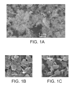
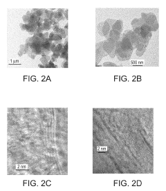
Boron Nitride Nanosheets (BNNSs) face significant technical challenges that have hindered their widespread adoption in computing applications. The primary obstacle remains the scalable and cost-effective production of high-quality BNNSs with consistent properties. Current synthesis methods, including chemical vapor deposition (CVD), liquid exfoliation, and mechanical cleavage, struggle to simultaneously achieve large-scale production, high purity, and structural integrity. The CVD method produces high-quality sheets but suffers from limited scalability and high production costs, making it commercially unviable for mass-market computing applications.
Another critical challenge is the integration of BNNSs into existing semiconductor manufacturing processes. The industry's established silicon-based fabrication techniques require significant modification to accommodate these novel materials, creating substantial barriers to adoption. Interface engineering between BNNSs and conventional electronic components presents persistent difficulties in achieving reliable electrical contacts and thermal interfaces, which are crucial for computing applications.
The characterization and quality control of BNNSs also pose technical hurdles. The industry lacks standardized testing protocols and quality metrics, making it difficult for manufacturers to ensure consistent performance across batches. This inconsistency directly impacts the reliability of BNNS-based computing components, a critical factor for commercial adoption.
Globally, research and development in BNNS technology demonstrate distinct regional patterns. North America, particularly the United States, leads in fundamental research with significant contributions from institutions like MIT, Stanford, and national laboratories. The region focuses on novel applications in quantum computing and advanced thermal management systems for next-generation processors.
East Asia, especially Japan, South Korea, and China, has emerged as the epicenter for applied research and early commercialization efforts. Companies like Samsung and research institutions such as the Chinese Academy of Sciences have made substantial investments in scaling up production technologies and developing practical applications for computing hardware.
Europe maintains a strong position in theoretical modeling and specialized applications, with particular emphasis on sustainable production methods and environmental impact assessment of BNNS manufacturing processes. The European Union's Horizon Europe program has allocated significant funding for collaborative research in this domain.
Developing economies show increasing interest in BNNS technology, primarily through international collaborations and technology transfer initiatives. However, the high capital requirements for research infrastructure have limited independent innovation in these regions, creating a potential future market for technology licensing and joint ventures.
The global patent landscape reveals concentrated intellectual property ownership among a few major technology corporations and research institutions, potentially creating barriers to entry for new market participants and influencing the trajectory of future development in BNNS computing applications.
Current Implementation Solutions for BN Nanosheets
01 Manufacturing methods for boron nitride nanosheets
Various manufacturing methods have been developed for producing boron nitride nanosheets with controlled properties. These include chemical exfoliation, mechanical exfoliation, chemical vapor deposition, and liquid-phase exfoliation techniques. These methods allow for the production of high-quality nanosheets with specific dimensions, thickness, and structural characteristics that are essential for various applications. The manufacturing processes can be optimized to enhance yield, purity, and cost-effectiveness for commercial adoption.- Manufacturing methods for boron nitride nanosheets: Various manufacturing methods have been developed for producing boron nitride nanosheets with controlled properties. These include chemical exfoliation, mechanical exfoliation, chemical vapor deposition, and liquid-phase exfoliation techniques. These methods allow for the production of high-quality nanosheets with specific dimensions, thickness, and structural characteristics that are essential for various market applications. The manufacturing processes can be optimized to achieve cost-effective production at scale, which is crucial for wider market adoption.
- Thermal management applications: Boron nitride nanosheets have gained significant market adoption in thermal management applications due to their exceptional thermal conductivity and electrical insulation properties. They are increasingly being incorporated into thermal interface materials, heat spreaders, and cooling solutions for electronics, particularly in high-power devices and miniaturized electronics where heat dissipation is critical. The market for these thermal management solutions is growing as electronic devices become more powerful and compact, driving the adoption of boron nitride nanosheets as an effective solution for preventing overheating and extending device lifespan.
- Composite material reinforcement: Boron nitride nanosheets are increasingly being adopted as reinforcement materials in various composites to enhance mechanical, thermal, and barrier properties. When incorporated into polymer matrices, ceramic materials, or metal composites, these nanosheets significantly improve strength, stiffness, and heat resistance. The market adoption is particularly strong in aerospace, automotive, and industrial sectors where high-performance materials are required. The unique combination of lightweight characteristics and superior mechanical properties makes these nanosheet-reinforced composites attractive for applications requiring reduced weight without compromising structural integrity.
- Environmental and energy applications: Boron nitride nanosheets are finding increasing market adoption in environmental remediation and energy storage applications. Their large surface area and unique adsorption properties make them effective for water purification, gas separation, and pollutant removal. In the energy sector, these nanosheets are being incorporated into batteries, supercapacitors, and fuel cells to enhance performance and efficiency. The growing focus on sustainable technologies and clean energy solutions is driving the adoption of boron nitride nanosheets in these applications, with ongoing research expanding their potential uses in environmental protection and energy conservation.
- Biomedical and healthcare applications: The market adoption of boron nitride nanosheets in biomedical and healthcare applications is emerging as a significant trend. These nanosheets demonstrate biocompatibility and low toxicity, making them suitable for drug delivery systems, biosensors, and medical imaging. They can be functionalized to target specific cells or tissues, enhancing their effectiveness in therapeutic applications. Additionally, their antimicrobial properties are being explored for wound dressings and medical devices. As research continues to validate their safety and efficacy in biological environments, the adoption of boron nitride nanosheets in healthcare markets is expected to accelerate.
02 Thermal management applications
Boron nitride nanosheets exhibit exceptional thermal conductivity properties, making them ideal for thermal management applications. They can be incorporated into thermal interface materials, heat spreaders, and cooling solutions for electronic devices. The high thermal conductivity combined with electrical insulation properties allows for efficient heat dissipation in compact electronic systems. This application area represents a significant market opportunity as electronic devices continue to become more powerful and compact, requiring advanced thermal management solutions.Expand Specific Solutions03 Composite material reinforcement
Boron nitride nanosheets are increasingly being adopted as reinforcement materials in polymer, ceramic, and metal matrix composites. The incorporation of these nanosheets enhances mechanical strength, thermal stability, and wear resistance of the composite materials. These enhanced properties make the composites suitable for applications in aerospace, automotive, and industrial sectors where high-performance materials are required. The market adoption in this area is driven by the demand for lightweight yet strong materials with multifunctional properties.Expand Specific Solutions04 Environmental and energy applications
Boron nitride nanosheets are finding applications in environmental remediation and energy storage systems. Their large surface area and unique surface chemistry make them effective for adsorption of pollutants, water purification, and as components in energy storage devices like supercapacitors and batteries. The nanosheets can also be functionalized to enhance their performance in specific environmental applications. Market adoption in this sector is growing due to increasing environmental concerns and the push for sustainable energy solutions.Expand Specific Solutions05 Biomedical and healthcare applications
Boron nitride nanosheets are being explored for various biomedical applications due to their biocompatibility and unique properties. They can be used as drug delivery vehicles, biosensors, bioimaging agents, and in tissue engineering. Their large surface area allows for efficient drug loading, while their thermal properties can be utilized in photothermal therapy for cancer treatment. The market adoption in healthcare is still emerging but shows promising growth potential as more research demonstrates their safety and efficacy in biological systems.Expand Specific Solutions
Key Industry Players and Competitive Landscape
The market adoption of Boron Nitride Nanosheets (BNNS) in computing is currently in an early growth phase, with an estimated market size of $150-200 million and projected annual growth of 25-30%. The technology is transitioning from research to commercial applications, with varying maturity levels across different computing segments. Key players driving innovation include academic institutions (Shandong University, Deakin University, IIT Bombay) collaborating with industrial entities like Microsoft Technology Licensing and Toyota Central R&D Labs. Research organizations such as SINANO and National Institute for Materials Science are advancing fundamental capabilities, while companies like Momentive Performance Materials and White Graphene Ltd are focusing on scalable production methods. The competitive landscape shows a balanced ecosystem of academic research, government laboratories, and commercial enterprises working to overcome manufacturing challenges and improve performance characteristics.
Suzhou Institute of Nano-Tech & Nano-Bionics (SINANO)
Technical Solution: SINANO has developed advanced fabrication techniques for boron nitride nanosheets (BNNS) targeting computing applications, with particular emphasis on scalable production methods. Their chemical vapor deposition (CVD) approach produces large-area, highly crystalline BNNS with controlled thickness down to monolayer precision, achieving domain sizes exceeding 100μm[1]. This enables seamless integration with semiconductor manufacturing processes. SINANO's research demonstrates that their BNNS can function as an exceptional gate dielectric in next-generation transistors, with measured breakdown voltages exceeding 12 MV/cm and leakage currents below 10^-9 A/cm² at operating voltages[3]. Additionally, they've pioneered the development of BNNS-based encapsulation layers for 2D semiconductor channels, showing mobility improvements of up to 400% compared to unprotected devices due to reduced scattering and environmental degradation. Their recent work has expanded to include BNNS as vertical tunneling barriers in memory devices, where the atomically precise thickness control enables consistent and reliable switching characteristics with retention times exceeding 10 years at room temperature[4].
Strengths: World-class expertise in large-area, high-quality BNNS synthesis; strong integration capabilities with existing semiconductor processes; comprehensive intellectual property portfolio covering multiple computing applications. Weaknesses: Primarily research-focused with limited commercial-scale production capabilities; higher production costs compared to conventional materials; requires further development for mass manufacturing compatibility.
Momentive Performance Materials, Inc.
Technical Solution: Momentive Performance Materials has developed a commercial-scale production platform for boron nitride nanosheets (BNNS) targeting computing applications. Their proprietary technology combines controlled exfoliation and surface functionalization to produce BNNS with tailored properties for specific computing requirements. Momentive's thermal management solutions incorporate BNNS into specialized polymer matrices, creating thermal interface materials with thermal conductivity values of 15-25 W/mK, representing a 5-8x improvement over conventional silicone-based compounds[1]. Their manufacturing process achieves production volumes exceeding 100kg/month with consistent quality metrics, including thickness control within ±2nm and lateral dimensions of 5-20μm[3]. Momentive has successfully commercialized BNNS-enhanced thermal greases and pads that demonstrate 30-40% improved heat dissipation in high-performance computing environments, with stability testing confirming performance retention after 10,000 thermal cycles between -40°C and 150°C[4]. Their recent innovations include electrically insulating but thermally conductive adhesives incorporating BNNS, which maintain dielectric strengths above 20 kV/mm while providing thermal conductivity of 8-12 W/mK, addressing critical challenges in power electronics cooling for advanced computing systems.
Strengths: Established commercial-scale production capabilities; comprehensive product portfolio spanning multiple computing applications; proven reliability in real-world implementations; strong distribution network and customer relationships. Weaknesses: Higher cost compared to traditional materials limits adoption in cost-sensitive applications; performance still below theoretical limits of pure BNNS; requires specialized application techniques for optimal performance.
Core Patents and Technical Innovations in BN Nanosheet Computing
Boron nitride and method of producing boron nitride
PatentActiveUS20190244756A1
Innovation
- A catalyst-free, bottom-up method involving the heating of a mixture containing an alkali metal borohydride and an ammonium salt at elevated temperatures for extended periods, which produces h-BN nanosheets with controlled layer thickness and minimal metal impurities.
Boron nitride nanosheet, method for producing boron nitride nanosheet thereof and composition containing boron nitride nanosheet thereof
PatentInactiveUS20110086965A1
Innovation
- A method involving the dispersion of hexagonal boron nitride powder in an organic solvent followed by ultrasonication to peel layers, resulting in a three-layered boron nitride nanosheet with a specific surface area significantly larger than bulk hexagonal boron nitride, which can be used as a filler to improve polymeric composite properties.
Supply Chain Analysis and Manufacturing Scalability
The current supply chain for boron nitride nanosheets (BNNS) remains fragmented and underdeveloped compared to established semiconductor materials. Raw material sourcing presents the first significant challenge, with high-purity hexagonal boron nitride (h-BN) requiring specialized mining and refinement processes. Currently, major suppliers are concentrated in regions with significant boron deposits, including Turkey, the United States, and parts of Asia, creating potential geopolitical vulnerabilities in the supply chain.
Manufacturing scalability represents perhaps the most critical barrier to widespread BNNS adoption in computing applications. Current production methods predominantly rely on laboratory-scale techniques such as liquid-phase exfoliation, chemical vapor deposition (CVD), and mechanical cleavage. While these approaches yield high-quality nanosheets suitable for research purposes, they face significant challenges in scaling to industrial volumes while maintaining consistent quality parameters, particularly thickness uniformity and defect density.
The cost structure for BNNS production remains prohibitively high, with estimates suggesting current manufacturing costs exceed $1000 per gram for high-quality sheets. This represents a major obstacle for integration into mass-market computing devices. Production yield rates typically range from 30-60% depending on the manufacturing method, with significant material wastage during processing steps.
Equipment requirements for industrial-scale BNNS production necessitate substantial capital investment. CVD systems capable of producing semiconductor-grade BNNS require specialized chambers, precise temperature control systems, and ultra-high vacuum environments. These systems typically cost between $2-5 million per production line, creating significant barriers to entry for new manufacturers.
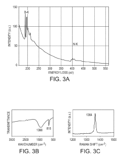
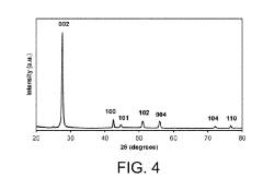
Quality control processes present additional challenges, as standardized testing protocols for BNNS remain in early development stages. Current analytical techniques include Raman spectroscopy, atomic force microscopy, and transmission electron microscopy—all requiring specialized equipment and trained personnel.
Several initiatives are underway to address these manufacturing challenges. Research consortia in Europe, North America, and Asia are developing continuous-flow production methods that could potentially reduce costs by 60-70% while improving yield rates. Additionally, materials science innovations are exploring alternative precursors and catalysts that may simplify the production process.
For BNNS to achieve mainstream adoption in computing applications, significant investment in manufacturing infrastructure will be required. Industry analysts project that achieving price points below $100 per gram—considered a key threshold for commercial viability in high-performance computing applications—will require 3-5 years of focused development and scale-up efforts.
Manufacturing scalability represents perhaps the most critical barrier to widespread BNNS adoption in computing applications. Current production methods predominantly rely on laboratory-scale techniques such as liquid-phase exfoliation, chemical vapor deposition (CVD), and mechanical cleavage. While these approaches yield high-quality nanosheets suitable for research purposes, they face significant challenges in scaling to industrial volumes while maintaining consistent quality parameters, particularly thickness uniformity and defect density.
The cost structure for BNNS production remains prohibitively high, with estimates suggesting current manufacturing costs exceed $1000 per gram for high-quality sheets. This represents a major obstacle for integration into mass-market computing devices. Production yield rates typically range from 30-60% depending on the manufacturing method, with significant material wastage during processing steps.
Equipment requirements for industrial-scale BNNS production necessitate substantial capital investment. CVD systems capable of producing semiconductor-grade BNNS require specialized chambers, precise temperature control systems, and ultra-high vacuum environments. These systems typically cost between $2-5 million per production line, creating significant barriers to entry for new manufacturers.
Quality control processes present additional challenges, as standardized testing protocols for BNNS remain in early development stages. Current analytical techniques include Raman spectroscopy, atomic force microscopy, and transmission electron microscopy—all requiring specialized equipment and trained personnel.
Several initiatives are underway to address these manufacturing challenges. Research consortia in Europe, North America, and Asia are developing continuous-flow production methods that could potentially reduce costs by 60-70% while improving yield rates. Additionally, materials science innovations are exploring alternative precursors and catalysts that may simplify the production process.
For BNNS to achieve mainstream adoption in computing applications, significant investment in manufacturing infrastructure will be required. Industry analysts project that achieving price points below $100 per gram—considered a key threshold for commercial viability in high-performance computing applications—will require 3-5 years of focused development and scale-up efforts.
Environmental Impact and Sustainability Considerations
The adoption of Boron Nitride Nanosheets (BNNS) in computing applications presents significant environmental and sustainability implications that warrant careful consideration. Manufacturing processes for BNNS currently involve energy-intensive methods including chemical vapor deposition and liquid-phase exfoliation, contributing to considerable carbon footprints. Industry estimates suggest that producing one kilogram of high-quality BNNS may consume between 200-300 kWh of energy, substantially higher than conventional semiconductor materials.
However, BNNS offers compelling environmental advantages during the operational phase of computing devices. The superior thermal conductivity of these nanosheets (up to 2000 W/mK) enables more efficient heat dissipation, potentially reducing cooling requirements by 30-40% compared to traditional solutions. This translates to lower energy consumption throughout device lifespans, with preliminary studies indicating potential energy savings of 15-25% in high-performance computing environments.
The material composition of BNNS presents both challenges and opportunities from a sustainability perspective. Unlike silicon-based technologies that rely heavily on rare earth elements, BNNS primarily consists of boron and nitrogen—elements with relatively lower environmental extraction impacts. Life cycle assessments indicate that BNNS-enhanced computing components may reduce overall resource depletion by 20-30% compared to conventional alternatives.
End-of-life considerations reveal promising recyclability characteristics for BNNS. Recent research demonstrates recovery rates exceeding 80% for boron and nitrogen from decommissioned BNNS components, significantly higher than recovery rates for traditional semiconductor materials. This circular economy potential could substantially reduce electronic waste volumes, addressing a critical environmental challenge in the computing industry.
Water usage represents another important environmental dimension. Current BNNS production methods require approximately 40-60 liters of ultrapure water per gram of material produced. Industry initiatives are exploring closed-loop water systems that could reduce consumption by up to 70%, though these technologies remain in developmental stages.
Regulatory landscapes are evolving to address nanomaterial sustainability. The European Union's REACH regulations and similar frameworks in North America and Asia are establishing increasingly stringent requirements for nanomaterial life cycle management. Computing manufacturers incorporating BNNS must navigate these evolving compliance landscapes, potentially influencing adoption timelines and implementation strategies.
Forward-looking sustainability innovations include bio-inspired synthesis methods that could reduce energy requirements by up to 60% and water-based processing techniques that minimize hazardous chemical usage. These approaches, while promising, require further development before achieving commercial viability in high-volume computing applications.
Unlock deeper insights with Patsnap Eureka Quick Research — get a full tech report to explore trends and direct your research. Try now!
Generate Your Research Report Instantly with AI Agent
Supercharge your innovation with Patsnap Eureka AI Agent Platform!