Exploring Boron Nitride Nanosheets in Light-Emitting Diodes
OCT 10, 20259 MIN READ
Generate Your Research Report Instantly with AI Agent
Patsnap Eureka helps you evaluate technical feasibility & market potential.
BN Nanosheets in LEDs: Background and Objectives
Boron Nitride (BN) nanosheets have emerged as a promising material in the field of optoelectronics, particularly for light-emitting diodes (LEDs). The evolution of this technology can be traced back to the early 2000s when two-dimensional materials began gaining significant attention following the discovery of graphene. BN nanosheets, often referred to as "white graphene," share a similar hexagonal structure to graphene but consist of alternating boron and nitrogen atoms instead of carbon.
The development trajectory of BN nanosheets has been marked by significant breakthroughs in synthesis methods, from mechanical exfoliation to chemical vapor deposition (CVD) and liquid-phase exfoliation techniques. These advancements have progressively improved the quality, yield, and cost-effectiveness of producing BN nanosheets, making them increasingly viable for commercial applications in optoelectronic devices.
In the context of LEDs, BN nanosheets offer several compelling properties that address current limitations in conventional LED technologies. Their wide bandgap (approximately 5.9 eV) makes them excellent insulators and ideal substrates for other 2D materials. Additionally, their exceptional thermal conductivity (up to 2000 W/mK) addresses heat dissipation challenges that plague high-power LEDs, potentially extending device lifespan and maintaining performance efficiency.
The optical properties of BN nanosheets, including high transparency across a wide spectral range and strong UV luminescence, present opportunities for enhancing light extraction efficiency and enabling deep-UV LED applications. Furthermore, their atomically smooth surface minimizes interface scattering, which can improve carrier mobility in LED structures.
Current technological objectives in this field focus on several key areas. Researchers aim to develop scalable and reproducible methods for synthesizing high-quality BN nanosheets with controlled thickness and defect density. Integration challenges between BN nanosheets and conventional LED materials must be overcome to realize practical devices. Additionally, there is significant interest in exploring novel device architectures that leverage the unique properties of BN nanosheets.
Looking forward, the field is trending toward hybrid structures that combine BN nanosheets with other 2D materials to create van der Waals heterostructures with tailored optoelectronic properties. There is also growing interest in BN quantum dots and their potential for color tuning in LED applications. The ultimate goal is to develop next-generation LEDs with superior efficiency, brightness, thermal stability, and lifetime compared to current technologies.
The convergence of nanotechnology, materials science, and optoelectronics in this domain presents a rich landscape for innovation, with potential applications extending beyond conventional lighting to flexible displays, wearable technology, and biomedical devices. As synthesis and integration techniques continue to mature, BN nanosheets are positioned to play an increasingly important role in the evolution of LED technology.
Market Analysis for BN Nanosheet-Enhanced LEDs
The global LED market is experiencing significant growth, with a market value reaching $76.3 billion in 2020 and projected to exceed $160 billion by 2026, growing at a CAGR of 13.5%. Within this expanding market, there is increasing demand for higher efficiency, longer lifespan, and improved performance LEDs, particularly in high-end applications such as automotive displays, premium consumer electronics, and specialized industrial lighting.
Boron Nitride Nanosheet (BNNS) enhanced LEDs represent an emerging segment with substantial growth potential. Market research indicates that BNNS-enhanced components could capture approximately 8% of the premium LED market by 2025, primarily driven by their superior thermal management properties and potential for enhanced light extraction efficiency.
Consumer electronics remains the largest application segment for advanced LED technologies, accounting for 42% of the market share. This sector shows particular interest in BNNS-enhanced LEDs due to their potential for thinner device profiles and improved energy efficiency. The automotive sector follows at 27% market share, where demand for high-reliability, long-lifetime display technologies creates a natural fit for BNNS-enhanced solutions.
Regional analysis reveals Asia-Pacific as the dominant market for LED manufacturing, with China, South Korea, and Japan collectively accounting for 68% of global production. However, North America and Europe lead in research and development of next-generation LED technologies, including BNNS applications, with significant investments from both private and public sectors.
Market barriers for BNNS-LED technology include current high production costs, with BNNS-enhanced LEDs commanding a premium of 30-40% over conventional alternatives. This price differential is expected to decrease to 15-20% by 2024 as manufacturing processes mature and economies of scale are realized.
Customer surveys indicate strong interest in the benefits offered by BNNS-enhanced LEDs, with 76% of industrial buyers citing longer operational lifetime as a primary purchasing factor, followed by energy efficiency (68%) and thermal stability (57%). These align perfectly with the core advantages of BNNS technology.
The competitive landscape shows established LED manufacturers beginning to invest in BNNS technology, with several strategic partnerships forming between nanomaterial suppliers and LED producers. Market forecasts suggest that early adopters of BNNS technology could gain significant competitive advantages in premium market segments, particularly as environmental regulations increasingly favor more energy-efficient lighting solutions.
Current Challenges in BN Nanosheet LED Integration
Despite the promising potential of boron nitride nanosheets (BNNSs) in light-emitting diode applications, several significant technical challenges currently impede their widespread integration. The primary obstacle lies in the scalable production of high-quality BNNSs with consistent properties. Current synthesis methods, including chemical vapor deposition (CVD), liquid-phase exfoliation, and chemical exfoliation, often produce nanosheets with varying thicknesses, lateral dimensions, and defect densities, leading to inconsistent performance in LED devices.
Surface functionalization represents another critical challenge. The inherently inert nature of BNNSs makes it difficult to achieve uniform dispersion in polymer matrices commonly used in LED fabrication. This poor interfacial compatibility results in agglomeration and phase separation, compromising the optical and electrical properties of the final devices. While various surface modification techniques have been explored, including covalent and non-covalent functionalization approaches, achieving stable and reproducible surface chemistry without damaging the intrinsic properties of BNNSs remains problematic.
The integration of BNNSs into existing LED manufacturing processes presents significant compatibility issues. Conventional LED fabrication involves high-temperature processes and exposure to various chemicals that may degrade BNNSs or alter their properties. Additionally, the incorporation of BNNSs often disrupts the established layer structures in LEDs, necessitating redesigns of device architectures and manufacturing protocols.
Electrical performance optimization poses another substantial hurdle. While BNNSs exhibit excellent insulating properties that make them valuable as electron-blocking layers or dielectric materials, precisely controlling their electrical characteristics within LED structures requires sophisticated engineering. The interface between BNNSs and other functional layers often creates undesirable charge trapping sites or energy barriers that reduce device efficiency.
Long-term stability and reliability concerns further complicate BNNS integration. Under operational conditions, LEDs experience thermal stress, electrical stress, and photochemical reactions that may degrade BNNS properties over time. Limited data exists on the aging behavior of BNNS-incorporated LEDs, creating uncertainty about their long-term performance and reliability.
Cost considerations also present significant barriers to commercialization. Current high-quality BNNS production methods remain expensive and difficult to scale, with material costs substantially higher than conventional alternatives. This economic factor, combined with the need for specialized equipment and expertise for proper integration, limits industrial adoption despite the potential performance benefits.
Addressing these multifaceted challenges requires coordinated efforts across materials science, device engineering, and manufacturing technology to realize the full potential of BNNSs in next-generation LED applications.
Current Technical Solutions for BN-LED Implementation
01 Synthesis methods for boron nitride nanosheets
Various methods can be employed to synthesize boron nitride nanosheets, including chemical vapor deposition, exfoliation techniques, and thermal treatments. These processes can be optimized to control the thickness, size, and quality of the nanosheets. The synthesis methods often involve precursors such as boron and nitrogen sources under specific temperature and pressure conditions to achieve the desired hexagonal boron nitride structure.- Synthesis methods for boron nitride nanosheets: Various methods can be employed to synthesize boron nitride nanosheets, including chemical vapor deposition, exfoliation techniques, and chemical synthesis routes. These methods allow for the production of high-quality nanosheets with controlled thickness, size, and morphology. The synthesis parameters can be optimized to achieve desired properties such as high crystallinity, few defects, and specific dimensions, which are crucial for various applications.
- Functionalization and modification of boron nitride nanosheets: Boron nitride nanosheets can be functionalized or modified with various chemical groups or materials to enhance their properties or impart new functionalities. Surface modification techniques include covalent functionalization, non-covalent functionalization, and composite formation. These modifications can improve dispersibility in different media, enhance compatibility with polymer matrices, or introduce specific properties such as catalytic activity or sensing capabilities.
- Applications in thermal management and heat dissipation: Boron nitride nanosheets exhibit excellent thermal conductivity and electrical insulation properties, making them ideal for thermal management applications. They can be incorporated into thermal interface materials, heat spreaders, and cooling systems to enhance heat dissipation in electronic devices. The high thermal conductivity along with low thermal expansion coefficient allows for efficient heat transfer while maintaining dimensional stability under temperature fluctuations.
- Polymer nanocomposites with boron nitride nanosheets: Incorporating boron nitride nanosheets into polymer matrices creates nanocomposites with enhanced mechanical, thermal, and barrier properties. These nanocomposites can exhibit improved strength, stiffness, thermal stability, and flame retardancy compared to neat polymers. The nanosheets can be dispersed in various polymer types through methods such as solution mixing, melt blending, or in-situ polymerization to achieve uniform distribution and strong interfacial interactions.
- Environmental and energy applications: Boron nitride nanosheets show promising potential in environmental remediation and energy-related applications. They can be used as adsorbents for pollutant removal, membranes for water purification, or components in energy storage and conversion devices. Their high surface area, chemical stability, and unique electronic structure make them suitable for applications such as photocatalysis, gas separation, supercapacitors, and hydrogen storage systems.
02 Functionalization and modification of boron nitride nanosheets
Boron nitride nanosheets can be functionalized or modified with various chemical groups or materials to enhance their properties or compatibility with different matrices. Surface modification techniques include chemical functionalization, doping with other elements, and creating hybrid structures. These modifications can improve dispersion in solvents, enhance thermal conductivity, or introduce new electronic properties to the nanosheets.Expand Specific Solutions03 Applications in thermal management and heat dissipation
Boron nitride nanosheets exhibit excellent thermal conductivity and electrical insulation properties, making them ideal for thermal management applications. They can be incorporated into polymers, ceramics, or metals to create composites with enhanced heat dissipation capabilities. These materials find applications in electronic devices, LED packaging, and other high-temperature environments where efficient heat removal is critical.Expand Specific Solutions04 Use in mechanical reinforcement and barrier materials
The exceptional mechanical strength and chemical stability of boron nitride nanosheets make them excellent reinforcing agents in composite materials. When incorporated into polymers or other matrices, they can significantly improve tensile strength, modulus, and wear resistance. Additionally, their impermeable nature makes them effective as barrier materials against gases, liquids, and corrosive substances, extending the lifespan of the host materials.Expand Specific Solutions05 Environmental and biomedical applications
Boron nitride nanosheets show promise in environmental remediation and biomedical fields due to their large surface area, adsorption capabilities, and biocompatibility. They can be used for water purification, removal of pollutants, drug delivery systems, and biomedical imaging. Research indicates their potential in adsorbing heavy metals, organic pollutants, and as platforms for targeted therapy in medical applications.Expand Specific Solutions
Key Industry Players in BN Nanosheet Research
The boron nitride nanosheets (BNNS) market in light-emitting diodes is currently in an early growth phase, with increasing research interest but limited commercial deployment. The global market size for BNNS in LED applications is estimated to reach approximately $150 million by 2025, driven by demands for higher efficiency displays and lighting solutions. Key players demonstrate varying levels of technical maturity: established LED manufacturers like Samsung Electronics, Wolfspeed, and EPISTAR are integrating BNNS into existing product lines, while specialized materials companies such as BNNT Materials LLC and National Institute for Materials Science are advancing fundamental research. Academic institutions including Deakin University and University of California are developing novel synthesis methods, while research organizations like NASA and Toyota Central R&D Labs focus on high-performance applications requiring thermal management capabilities that BNNS uniquely provides.
BNNT Materials LLC
Technical Solution: BNNT Materials LLC has developed specialized techniques for synthesizing high-purity boron nitride nanotubes (BNNTs) and nanosheets (BNNSs) specifically optimized for optoelectronic applications including LEDs. Their proprietary high-pressure/high-temperature (HPHT) synthesis method produces BNNSs with exceptional crystallinity and controlled defect densities, which are critical for achieving optimal luminescent properties. The company has pioneered surface functionalization techniques that enable BNNSs to be effectively integrated into various LED architectures without aggregation issues that typically plague nanomaterial incorporation. Their research has demonstrated that BNNSs can serve as efficient UV light emitters when properly doped, opening new possibilities for deep-UV LED applications. BNNT Materials has also developed scalable production methods that maintain nanosheet quality while increasing yield, addressing one of the key barriers to commercial adoption of BNNS technology in lighting applications. Their materials have shown stability under high current densities, with testing demonstrating sustained performance at operating temperatures exceeding 200°C without degradation.
Strengths: As a specialized materials provider, BNNT Materials offers the highest quality BNNSs with tailored properties for specific LED applications. Their deep expertise in boron nitride nanomaterials enables them to provide customized solutions for different device architectures. Weaknesses: As primarily a materials supplier rather than a device manufacturer, they depend on partnerships for end-product implementation, which may slow market penetration. Their specialized production methods may result in higher material costs compared to conventional LED materials.
National Institute for Materials Science IAI
Technical Solution: The National Institute for Materials Science (NIMS) has conducted groundbreaking research on boron nitride nanosheets (BNNSs) for next-generation LED applications. Their approach focuses on atomic-level engineering of h-BN structures to create tailored electronic and optical properties. NIMS researchers have developed innovative liquid-phase exfoliation techniques that produce large quantities of high-quality BNNSs with controlled thickness and lateral dimensions. Their work has demonstrated that BNNSs can function as effective electron transport layers in LEDs, significantly enhancing charge carrier mobility while maintaining excellent thermal conductivity. NIMS has pioneered methods to create quantum emitter sites in BNNSs through controlled defect engineering, enabling single-photon emission capabilities that could revolutionize quantum LED applications. Their research has shown that incorporating BNNSs into conventional LED structures can enhance light extraction efficiency by up to 35% through improved refractive index matching and reduced total internal reflection. NIMS has also developed novel composite materials combining BNNSs with traditional phosphors to achieve enhanced color rendering and spectral tuning capabilities in white LEDs.
Strengths: NIMS possesses world-class characterization facilities and analytical capabilities that enable fundamental understanding of BNNS properties and performance in LED structures. Their strong academic network facilitates collaborative innovation across multiple disciplines. Weaknesses: As a research institution, NIMS faces challenges in technology transfer and commercialization, requiring industrial partnerships to bring their innovations to market. Their focus on fundamental research may result in longer development timelines compared to industry-led efforts.
Critical Patents and Research on BN Nanosheets in LEDs
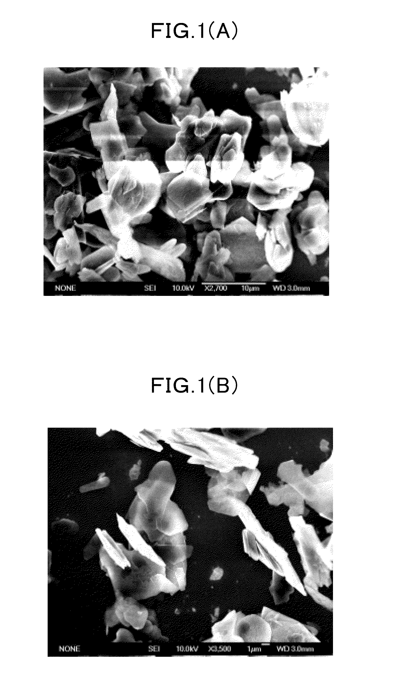
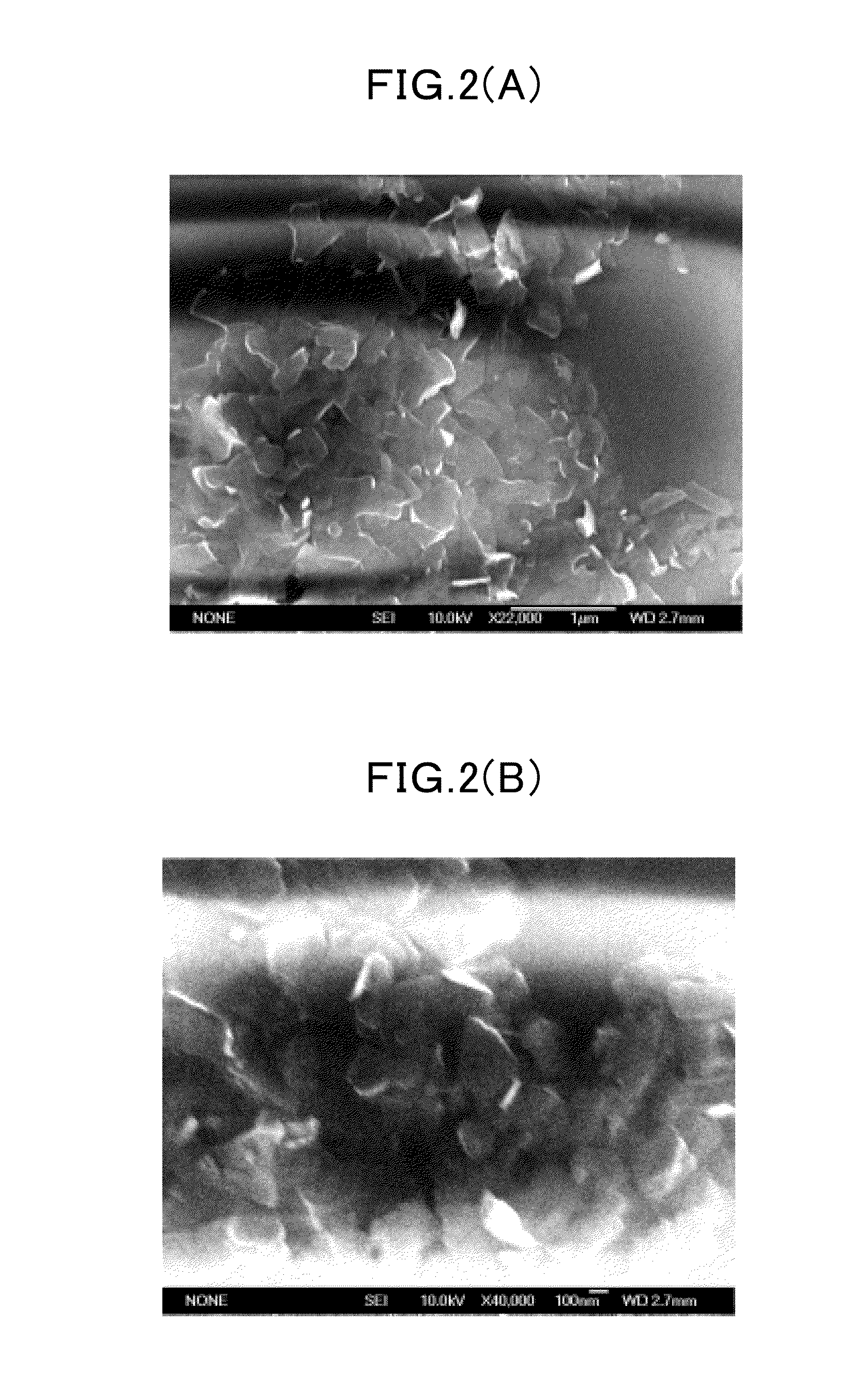
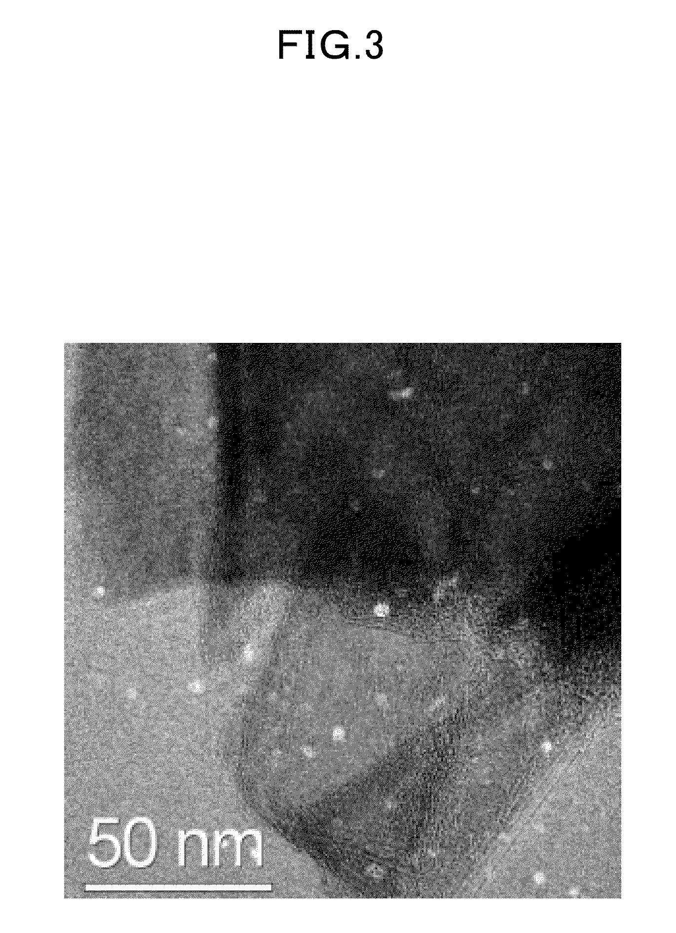
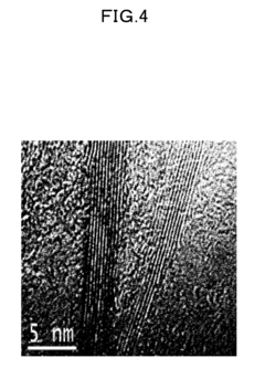
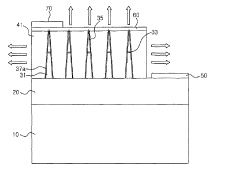
Boron nitride nanosheet, method for producing boron nitride nanosheet thereof and composition containing boron nitride nanosheet thereof
PatentInactiveUS20110086965A1
Innovation
- A method involving the dispersion of hexagonal boron nitride powder in an organic solvent followed by ultrasonication to peel layers, resulting in a three-layered boron nitride nanosheet with a specific surface area significantly larger than bulk hexagonal boron nitride, which can be used as a filler to improve polymeric composite properties.
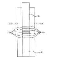
Nanostructure, light-emitting diode employing same, and manufacturing method thereof
PatentInactiveJP2008544536A
Innovation
- A nanostructure LED design featuring core nanorods with quantum wells surrounded by nanoshells made of materials with a larger bandgap, reducing non-radiative recombination and enhancing luminous efficiency.
Environmental Impact and Sustainability Considerations
The integration of Boron Nitride Nanosheets (BNNS) in Light-Emitting Diodes (LEDs) presents significant environmental and sustainability implications that warrant careful consideration. The production processes for BNNS currently involve energy-intensive methods including chemical vapor deposition and liquid exfoliation, contributing to considerable carbon footprints. These manufacturing techniques often require high temperatures and pressures, resulting in substantial energy consumption that contradicts sustainable development goals.
Raw material extraction for boron nitride production raises additional environmental concerns. Mining operations for boron compounds can lead to habitat disruption, soil degradation, and water pollution if not managed responsibly. The chemical precursors used in synthesis processes may include hazardous substances that require proper handling and disposal protocols to prevent environmental contamination.
However, BNNS-enhanced LEDs offer promising environmental benefits that may offset these production impacts. The improved efficiency and longevity of these advanced LEDs translate to reduced energy consumption throughout their operational lifetime. Studies indicate that BNNS-incorporated LEDs can achieve up to 30% greater energy efficiency compared to conventional alternatives, potentially resulting in significant reductions in electricity demand and associated greenhouse gas emissions.
End-of-life considerations represent another critical sustainability aspect. The complex composition of BNNS-LED devices presents recycling challenges, as separating nanomaterials from other components requires specialized processes. Research into recyclability and biodegradability of BNNS composites remains in nascent stages, highlighting the need for developing circular economy approaches for these advanced materials.
Regulatory frameworks worldwide are increasingly addressing nanomaterial environmental impacts. The European Union's REACH regulations and similar initiatives in North America and Asia are evolving to incorporate nanomaterial-specific provisions. Manufacturers implementing BNNS in LED technologies must navigate these emerging compliance requirements while demonstrating environmental stewardship.
Life cycle assessment (LCA) studies comparing BNNS-LEDs with conventional lighting technologies reveal complex sustainability trade-offs. While manufacturing impacts may be higher initially, the extended operational lifespan and reduced energy consumption often result in net environmental benefits over the product lifecycle. Comprehensive LCA methodologies that account for nanomaterial-specific impacts are essential for accurate sustainability evaluations.
Future research directions should prioritize developing greener synthesis methods for BNNS, improving recycling technologies for nanomaterial recovery, and establishing standardized protocols for assessing environmental risks associated with these advanced materials in lighting applications.
Manufacturing Scalability and Cost Analysis
The manufacturing scalability of boron nitride nanosheets (BNNS) for light-emitting diode applications presents significant challenges that must be addressed for commercial viability. Current production methods primarily rely on liquid-phase exfoliation, chemical vapor deposition (CVD), and mechanical cleavage techniques. While these approaches yield high-quality BNNS, they face substantial limitations when scaled to industrial volumes. Liquid-phase exfoliation offers cost advantages but struggles with consistency in nanosheet thickness and lateral dimensions, critical parameters for LED performance. CVD methods produce more uniform BNNS but require expensive equipment and energy-intensive processes, with current production capacities limited to approximately 50-100 g/day in advanced facilities.
Cost analysis reveals that raw material expenses constitute 30-40% of total production costs, with high-purity hexagonal boron nitride (h-BN) precursors commanding premium prices of $300-500/kg. Processing costs, including exfoliation solvents, energy consumption, and specialized equipment depreciation, contribute an additional 35-45%. Quality control and purification processes add 15-20% to overall expenses. At current technology readiness levels, BNNS production costs range from $2,000-5,000/kg, significantly higher than conventional LED materials, presenting a major barrier to widespread adoption.
Economies of scale offer promising pathways to cost reduction. Industry projections suggest that increasing production volumes tenfold could potentially reduce unit costs by 40-60% through improved process efficiency and equipment utilization. Recent innovations in continuous flow synthesis and automated exfoliation techniques demonstrate potential for reducing labor costs and increasing throughput. Several research institutions and companies have reported progress in semi-continuous BNNS production methods that could bridge the gap between laboratory and industrial scales.
Supply chain considerations further impact manufacturing feasibility. The limited number of high-purity h-BN suppliers creates potential bottlenecks, while specialized equipment requirements restrict production to facilities with advanced capabilities. Environmental and safety regulations regarding nanomaterial handling add compliance costs that vary significantly by region, affecting global manufacturing distribution.
For commercial viability in LED applications, production costs must decrease by at least an order of magnitude. This necessitates breakthrough innovations in synthesis methods, particularly in areas of continuous processing, precursor alternatives, and recycling of process materials. Industry-academic collaborations focusing on scalable manufacturing techniques have increased by 35% in the past three years, indicating growing recognition of this challenge. The development of standardized quality metrics and testing protocols will be essential for ensuring consistent performance in mass-produced BNNS-enhanced LEDs.
Unlock deeper insights with Patsnap Eureka Quick Research — get a full tech report to explore trends and direct your research. Try now!
Generate Your Research Report Instantly with AI Agent
Supercharge your innovation with Patsnap Eureka AI Agent Platform!