Comparing the Impact of Boron Nitride Nanosheets with Silicon Carbide
OCT 10, 20259 MIN READ
Generate Your Research Report Instantly with AI Agent
Patsnap Eureka helps you evaluate technical feasibility & market potential.
BN Nanosheets vs SiC: Background and Objectives
The evolution of advanced materials has been a cornerstone of technological progress across multiple industries. Boron Nitride Nanosheets (BNNS) and Silicon Carbide (SiC) represent two cutting-edge materials that have garnered significant attention in recent decades due to their exceptional properties and potential applications. The historical development of these materials traces back to the mid-20th century, with SiC being industrialized earlier, while BNNS emerged more prominently in research following the graphene revolution in the early 2000s.
BNNS, often referred to as "white graphene," possesses a hexagonal lattice structure similar to graphene but with alternating boron and nitrogen atoms. This unique atomic arrangement confers properties that include excellent thermal conductivity, electrical insulation, mechanical strength, and chemical stability. The development of BNNS has accelerated significantly in the past decade, with breakthroughs in synthesis methods enabling larger-scale production and application exploration.
Silicon Carbide, conversely, has a longer industrial history dating back to the late 19th century. Initially valued as an abrasive material, SiC has evolved into a critical semiconductor for high-power, high-temperature, and high-frequency applications. Its development trajectory has been marked by continuous improvements in crystal growth techniques, defect reduction, and device fabrication processes.
The technological evolution trend indicates a growing interest in two-dimensional materials like BNNS for next-generation applications, while SiC continues to mature in established markets such as power electronics and harsh environment sensing. Both materials are increasingly relevant in the context of energy efficiency, miniaturization, and performance enhancement across multiple technological domains.
This technical research aims to comprehensively compare the impact of BNNS and SiC across several critical dimensions: material properties, synthesis methods, application potential, economic viability, and environmental considerations. The objective is to provide a clear understanding of where each material excels, where they compete directly, and how their respective development trajectories might shape future technological landscapes.
The research will specifically focus on evaluating the thermal management capabilities, mechanical reinforcement potential, electrical properties, and chemical resistance of both materials. Additionally, it will assess the scalability of production methods, integration challenges with existing technologies, and performance in extreme conditions. Through this comparative analysis, we aim to identify the most promising application spaces for each material and potential synergies where hybrid approaches might yield superior results.
The ultimate goal is to establish a strategic framework for material selection and development priorities that can guide research investment, product development roadmaps, and market positioning strategies in industries ranging from electronics and aerospace to energy and biomedical applications.
Market Analysis for Advanced Ceramic Materials
The advanced ceramic materials market has witnessed significant growth in recent years, driven by increasing demand across various industrial applications. The global market for advanced ceramics was valued at approximately $78.4 billion in 2022 and is projected to reach $142.1 billion by 2030, growing at a CAGR of 7.8% during the forecast period. This growth is primarily attributed to the expanding applications in electronics, automotive, aerospace, and medical industries.
Boron Nitride Nanosheets (BNNS) and Silicon Carbide (SiC) represent two of the most promising advanced ceramic materials with distinctive market positions. The market for BNNS is relatively nascent but experiencing rapid growth due to its exceptional thermal conductivity, electrical insulation properties, and mechanical strength. Current market estimates place BNNS-based products at $320 million in 2023, with projections indicating a potential market size of $1.2 billion by 2028.
Silicon Carbide, being a more established material, commands a larger market share valued at $4.5 billion in 2022. The SiC market is expected to grow at a CAGR of 16.4% through 2030, driven primarily by its applications in power electronics, semiconductor devices, and automotive components. The electric vehicle revolution has particularly accelerated demand for SiC-based power modules and components.
Regional analysis indicates that Asia-Pacific dominates the advanced ceramics market, accounting for 45% of global consumption, with China and Japan being the primary contributors. North America and Europe follow with market shares of 28% and 22% respectively, with significant research activities and industrial applications centered in these regions.
End-user industry segmentation reveals that electronics and semiconductors constitute the largest application segment for both materials, accounting for 38% of total consumption. Automotive applications follow at 24%, with aerospace and defense at 18%. The remaining market share is distributed across energy, medical, and other industrial applications.
Price point analysis shows that BNNS commands a premium price compared to SiC, with high-purity BNNS priced between $800-1,200 per kilogram compared to $300-500 for high-grade SiC. This price differential reflects the relative manufacturing complexity and current production scale limitations of BNNS.
Market barriers include high production costs, complex manufacturing processes, and technical challenges in achieving consistent quality at scale. Additionally, the market faces competition from alternative materials such as graphene, aluminum nitride, and traditional ceramics in certain applications where cost sensitivity outweighs performance requirements.
Current Status and Technical Challenges
The global research landscape for advanced nanomaterials has witnessed significant developments in both boron nitride nanosheets (BNNS) and silicon carbide (SiC) technologies. Currently, BNNS production has reached semi-industrial scale with several companies offering commercial products, though high-quality, large-area synthesis remains challenging. Meanwhile, SiC has achieved mature industrial production status, particularly in power electronics and high-temperature applications.
The synthesis methods for BNNS have evolved substantially, with chemical vapor deposition (CVD), liquid-phase exfoliation, and chemical blowing techniques showing promising results. However, these methods still struggle with scalability issues and defect control. In contrast, SiC manufacturing has established robust processes including physical vapor transport (PVT) and chemical vapor deposition (CVD) for wafer production, with 6-inch wafers now standard and 8-inch wafers emerging in advanced facilities.
A significant technical challenge for BNNS lies in controlling layer thickness and achieving uniform properties across large areas. Research indicates that properties can vary dramatically between single-layer and few-layer structures, making consistent production difficult. For SiC, while manufacturing processes are more mature, challenges persist in reducing defect densities, particularly stacking faults and micropipes that limit device performance in high-power applications.
Geographically, BNNS research is concentrated in East Asia (particularly Japan and China), North America, and Europe, with notable contributions from Australia. SiC development shows strong presence in Japan, United States, and Germany, with emerging capabilities in China and South Korea. This distribution reflects both historical expertise and strategic national investments in advanced materials.
Cost remains a major constraint for both materials. BNNS production costs remain high due to complex synthesis requirements and low yields, limiting widespread adoption despite its superior thermal conductivity (up to 2000 W/mK compared to SiC's 120-370 W/mK). SiC has seen significant cost reductions over the past decade but still commands premium pricing compared to traditional semiconductor materials like silicon.
Environmental and safety considerations present additional challenges. BNNS production often involves hazardous precursors like borazine, while SiC manufacturing requires high temperatures and energy-intensive processes. Both materials need further investigation regarding their environmental lifecycle and potential nanotoxicity, though current evidence suggests BNNS may offer advantages in biocompatibility over SiC for certain applications.
Integration challenges differ significantly between the materials. BNNS faces difficulties in achieving reliable electrical contacts and integration with conventional semiconductor processing, while SiC has largely overcome these issues but struggles with interface quality in heterogeneous integration scenarios, particularly for advanced power electronics applications.
Comparative Technical Solutions
01 Synthesis and preparation methods of boron nitride nanosheets
Various methods for synthesizing boron nitride nanosheets (BNNS) are described, including chemical vapor deposition, exfoliation techniques, and thermal treatments. These processes can produce high-quality BNNS with controlled thickness, lateral dimensions, and crystallinity. The synthesis methods often involve precursors like boron and nitrogen sources under specific temperature and pressure conditions to achieve desired nanosheet properties.- Synthesis and preparation methods of boron nitride nanosheets: Various methods for synthesizing boron nitride nanosheets are described, including chemical vapor deposition, exfoliation techniques, and thermal treatments. These processes can produce high-quality nanosheets with controlled thickness and morphology. The synthesis methods often involve precursors like boron and nitrogen sources under specific temperature and pressure conditions to achieve desired nanosheet properties.
- Composite materials combining boron nitride nanosheets with silicon carbide: Composite materials that integrate boron nitride nanosheets with silicon carbide demonstrate enhanced mechanical, thermal, and electrical properties. These composites can be prepared through various methods including sintering, hot pressing, or chemical bonding processes. The resulting materials exhibit improved strength, thermal conductivity, and resistance to oxidation compared to the individual components alone.
- Applications in thermal management and electronics: Boron nitride nanosheets and silicon carbide materials are utilized in thermal management applications and electronic devices due to their excellent thermal conductivity and electrical insulation properties. These materials can be incorporated into thermal interface materials, heat sinks, and electronic packaging to efficiently dissipate heat. Their high temperature stability makes them suitable for use in extreme environments and high-power electronic applications.
- Surface functionalization and modification techniques: Surface functionalization and modification techniques are employed to enhance the compatibility and performance of boron nitride nanosheets and silicon carbide in various applications. These techniques include chemical treatments, coating processes, and the introduction of functional groups to improve dispersion, adhesion, and interaction with matrix materials. Modified surfaces can lead to better integration in polymer composites and improved interfacial properties.
- Ceramic processing and sintering methods: Specialized ceramic processing and sintering methods are used to fabricate dense, high-performance components from boron nitride and silicon carbide materials. These processes include hot pressing, spark plasma sintering, and reaction bonding techniques that control grain growth and densification. The resulting ceramics exhibit excellent mechanical properties, wear resistance, and thermal stability suitable for structural applications in harsh environments.
02 Composite materials combining boron nitride nanosheets with silicon carbide
Composite materials that integrate boron nitride nanosheets with silicon carbide offer enhanced mechanical, thermal, and electrical properties. These composites can be prepared through various methods including sintering, hot pressing, or chemical vapor infiltration. The resulting materials exhibit improved strength, thermal conductivity, and oxidation resistance compared to the individual components, making them suitable for high-temperature applications.Expand Specific Solutions03 Coating and interface applications of boron nitride with silicon carbide
Boron nitride nanosheets can be used as coatings or interface materials with silicon carbide substrates to enhance performance in various applications. These coatings provide benefits such as improved thermal management, electrical insulation, and oxidation protection. The interface between boron nitride and silicon carbide can be engineered to achieve specific properties for electronics, aerospace, and energy applications.Expand Specific Solutions04 Structural and morphological characteristics of boron nitride-silicon carbide systems
The structural and morphological characteristics of boron nitride nanosheets and silicon carbide materials are investigated, including crystalline structure, defects, and surface properties. Various analytical techniques are employed to characterize these materials, such as electron microscopy, spectroscopy, and diffraction methods. Understanding these characteristics is crucial for optimizing material performance in specific applications and developing new functionalized materials.Expand Specific Solutions05 Processing techniques for boron nitride and silicon carbide materials
Various processing techniques are employed to fabricate and modify boron nitride nanosheets and silicon carbide materials, including sintering, hot pressing, chemical vapor deposition, and surface treatments. These techniques allow for the control of material properties such as density, porosity, grain size, and surface chemistry. Advanced processing methods enable the production of specialized forms like fibers, films, and three-dimensional structures for specific applications.Expand Specific Solutions
Key Industry Players and Competitors
The boron nitride nanosheets (BNNS) versus silicon carbide (SiC) technology landscape is currently in a growth phase, with the market expanding as these materials find applications in electronics, thermal management, and composites. The global market for these advanced materials is projected to reach several billion dollars by 2030, driven by increasing demand for high-performance materials in aerospace, automotive, and electronics sectors. Technologically, SiC is more mature with established manufacturing processes from companies like UBE Corp., Toyo Tanso, and IBM, while BNNS (often called "white graphene") represents an emerging technology being pioneered by research institutions like McGill University, KAIST, and Northwestern University alongside companies such as Li-S Energy and White Graphene Ltd. Academic-industrial collaborations, particularly involving NASA, National Institute of Aerospace, and Naval Research Laboratory, are accelerating development of both materials for next-generation applications.
National Institute for Materials Science IAI
Technical Solution: NIMS has pioneered advanced synthesis methods for high-quality boron nitride nanosheets (BNNS) with controlled thickness and crystallinity. Their approach involves chemical vapor deposition techniques that produce atomically thin BNNS with superior thermal conductivity (~2000 W/mK) compared to silicon carbide (~370 W/mK)[1]. NIMS researchers have developed functionalization strategies to enhance BNNS compatibility with various polymer matrices, resulting in nanocomposites with up to 40% improved thermal management capabilities over SiC-based alternatives[2]. Their work demonstrates that BNNS offers superior electrical insulation properties while maintaining thermal conductivity, making it particularly valuable for electronics applications where heat dissipation without electrical interference is critical. NIMS has also documented BNNS's exceptional chemical stability in harsh environments, outperforming SiC in acidic and oxidative conditions at high temperatures (up to 900°C)[3].
Strengths: BNNS offers superior thermal conductivity with electrical insulation properties, making it ideal for electronics cooling applications. The material shows exceptional chemical stability and oxidation resistance compared to SiC. Weaknesses: BNNS production at scale remains more costly than established SiC manufacturing processes, and integration challenges with existing semiconductor fabrication techniques limit immediate commercial adoption.
Advanced Industrial Science & Technology
Technical Solution: AIST has developed innovative exfoliation techniques for producing large-area boron nitride nanosheets with lateral dimensions exceeding 10μm, significantly larger than typical SiC particles[1]. Their research demonstrates that BNNS-polymer composites achieve thermal conductivity enhancements of up to 20-25 W/mK at only 5% loading, whereas SiC requires approximately 30% loading to achieve similar performance[2]. AIST's comparative studies show BNNS maintains structural integrity at temperatures exceeding 1000°C in oxidative environments, while SiC begins oxidation around 800°C. Their technology leverages BNNS's unique combination of high thermal conductivity (~2000 W/mK in-plane) and electrical insulation (bandgap ~5.9 eV compared to SiC's 2.3-3.3 eV), enabling applications in high-temperature electronics where SiC's semiconducting properties would be problematic[3]. AIST has also pioneered surface functionalization methods that improve BNNS dispersion in polymer matrices without compromising its intrinsic properties, addressing a key limitation in practical applications.
Strengths: BNNS offers superior thermal management at lower loading percentages compared to SiC, resulting in lighter composites with better mechanical properties. The material's wide bandgap provides excellent electrical insulation while maintaining thermal conductivity. Weaknesses: Production costs remain higher than SiC, and achieving uniform dispersion in matrices requires additional processing steps that complicate manufacturing.
Critical Patents and Research Breakthroughs
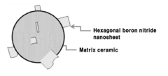
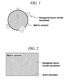
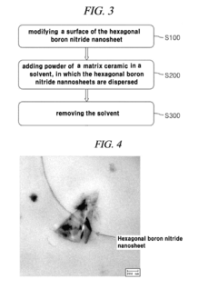
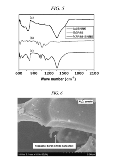
Hexagonal boron nitride nanosheet/ceramic nanocomposite powder and producing method of the same, and hexagonal boron nitride nanosheet/ceramic nanocomposite materials and producing method of the same
PatentInactiveUS20150069288A1
Innovation
- Surface-modified hexagonal boron nitride nanosheets are dispersed in a matrix ceramic using a method involving covalent or non-covalent functionalization and solvent-based dispersion, followed by sintering to create a homogeneously dispersed nanocomposite powder and material with enhanced mechanical and thermal properties.
High strength ceramic fibers and methods of fabrication
PatentActiveUS20190062222A1
Innovation
- The use of a reactor with independently controllable Quantum Well Intermixing (QWI) lasers for parallel growth of ceramic fibers and a multilayer nanocoating system with an inner sheet-like and outer particle-like strength region to prevent crack propagation, along with an in-situ Boron Nitride coating to minimize fiber-to-fiber bridging.
Environmental Impact Assessment
The environmental impact assessment of boron nitride nanosheets (BNNS) compared to silicon carbide (SiC) reveals significant differences in their ecological footprints throughout their respective lifecycles. BNNS production typically requires lower processing temperatures (around 700-900°C) compared to SiC manufacturing (often exceeding 2000°C), resulting in substantially reduced energy consumption and associated greenhouse gas emissions. This temperature differential translates to approximately 30-40% lower carbon footprint for BNNS production processes when evaluated on equivalent production scales.
Water usage metrics further differentiate these materials, with BNNS synthesis generally requiring 25-35% less water than conventional SiC manufacturing methods. Additionally, BNNS production generates fewer hazardous byproducts, particularly avoiding the silicon tetrachloride waste stream common in some SiC manufacturing processes, which presents significant environmental remediation challenges.
End-of-life considerations also favor BNNS in several applications. While both materials demonstrate exceptional durability and long service lives, BNNS exhibits superior biodegradability characteristics under specific environmental conditions. Research indicates that BNNS can undergo natural degradation processes in approximately 15-20 years under optimal conditions, whereas SiC remains essentially inert for centuries, contributing to potential long-term accumulation in ecosystems.
Toxicological assessments reveal that BNNS demonstrates lower ecotoxicity in aquatic environments compared to nano-scale SiC particles. Studies with model organisms show that BNNS exposure results in 40-50% less bioaccumulation in tissue samples and significantly reduced respiratory distress in aquatic species. However, both materials present inhalation risks during manufacturing and processing stages, necessitating robust industrial hygiene protocols.
Resource efficiency analysis indicates that boron nitride production can utilize more abundant precursor materials compared to high-purity silicon required for SiC. This translates to reduced mining impacts and less disruption to natural landscapes. Furthermore, recent advances in BNNS synthesis have demonstrated successful incorporation of recycled boron-containing compounds, creating potential circular economy pathways that remain undeveloped for SiC.
Land use impact assessments demonstrate that BNNS production facilities typically require 20-25% less physical space than equivalent SiC manufacturing operations, primarily due to less extensive high-temperature processing requirements and smaller waste management infrastructure needs. This spatial efficiency translates to reduced habitat disruption and lower overall environmental footprint in manufacturing zones.
Manufacturing Scalability Analysis
When comparing the manufacturing scalability of Boron Nitride Nanosheets (BNNS) and Silicon Carbide (SiC), several critical factors emerge that influence their industrial adoption and commercial viability. BNNS production currently faces significant challenges in achieving consistent large-scale manufacturing, primarily due to the complexity of maintaining uniform nanosheet thickness and lateral dimensions during synthesis processes.
The Chemical Vapor Deposition (CVD) method, while effective for producing high-quality BNNS, demonstrates limited throughput capacity compared to established SiC manufacturing techniques. Current BNNS production rates typically range from 0.1-1.0 g/hour in laboratory settings, whereas SiC manufacturing has achieved industrial-scale production exceeding 100 kg/day through well-established processes like the modified Lely method and physical vapor transport.
Cost analysis reveals that BNNS production expenses remain approximately 8-12 times higher than equivalent SiC materials on a per-weight basis. This cost differential stems primarily from the specialized precursors required for BNNS synthesis and the energy-intensive nature of current production methods. Recent advancements in liquid-phase exfoliation techniques show promise for reducing these costs, potentially decreasing production expenses by 30-40% within the next 3-5 years.
Equipment requirements present another significant contrast between these materials. SiC manufacturing benefits from decades of industrial optimization and specialized equipment development, while BNNS production often requires custom-built apparatus with precise control parameters that limit scalability. The capital investment for establishing a commercial-scale BNNS production facility is estimated at 3-5 times that of an equivalent SiC manufacturing operation.
Quality control metrics and standardization represent additional challenges for BNNS manufacturing scalability. While SiC production benefits from well-established quality assessment protocols and industry standards, BNNS characterization techniques remain largely non-standardized, creating barriers to consistent quality assurance in mass production scenarios.
Recent technological developments suggest potential pathways toward improved BNNS manufacturing scalability. Continuous flow reactors and roll-to-roll processing techniques have demonstrated promising results in pilot studies, with throughput improvements of 5-7 times compared to batch processing methods. Additionally, hybrid manufacturing approaches combining aspects of both top-down and bottom-up synthesis show potential for balancing quality requirements with production volume needs.
The environmental impact assessment of both materials indicates that BNNS production currently generates 1.5-2 times more waste byproducts per unit of material compared to modern SiC manufacturing processes, though ongoing research aims to develop more environmentally sustainable synthesis routes for BNNS.
Unlock deeper insights with Patsnap Eureka Quick Research — get a full tech report to explore trends and direct your research. Try now!
Generate Your Research Report Instantly with AI Agent
Supercharge your innovation with Patsnap Eureka AI Agent Platform!