Case Study: Fabrication Flow For An AFM Prototype Memory Chip
SEP 1, 20259 MIN READ
Generate Your Research Report Instantly with AI Agent
Patsnap Eureka helps you evaluate technical feasibility & market potential.
AFM Memory Technology Background and Objectives
Atomic Force Microscopy (AFM) memory technology represents a significant evolution in data storage systems, emerging from the broader field of scanning probe microscopy developed in the 1980s. This technology leverages nanoscale mechanical interactions between an ultra-sharp tip and a storage medium to read, write, and erase data at unprecedented densities. The fundamental principle involves creating physical indentations or alterations in a polymer or phase-change material substrate, which can be detected as binary information.
The historical trajectory of AFM memory development began with IBM's Millipede project in the late 1990s, which demonstrated the feasibility of using arrays of AFM tips for parallel data operations. This breakthrough established the foundation for high-density, non-volatile storage solutions that could potentially exceed the theoretical limits of conventional magnetic and flash memory technologies.
Current technical objectives for AFM prototype memory chips focus on achieving commercial viability through several key parameters. Primary goals include reaching data densities exceeding 1 Tbit/in², access speeds comparable to solid-state drives (under 10ms), and power consumption profiles suitable for mobile and edge computing applications. Additionally, researchers aim to develop fabrication processes compatible with existing semiconductor manufacturing infrastructure to facilitate eventual mass production.
The technology promises significant advantages in terms of data retention, with theoretical stability exceeding 10 years without power, and exceptional resistance to electromagnetic interference and radiation effects. These characteristics position AFM memory as particularly valuable for specialized applications in aerospace, defense, and critical infrastructure where data integrity under extreme conditions is paramount.
Recent advancements in materials science have expanded the potential of AFM memory, with research focusing on phase-change chalcogenides, ferroelectric polymers, and specialized carbon-based substrates. These materials offer improved mechanical durability, reduced tip wear, and enhanced signal-to-noise ratios during read operations.
The fabrication flow for AFM prototype memory chips represents a convergence of traditional semiconductor processing techniques with novel approaches specific to nanomechanical systems. Key challenges include the precise manufacturing of tip arrays with consistent dimensions at the nanometer scale, integration of sensing circuitry capable of detecting minute mechanical deflections, and development of wear-resistant coatings to extend operational lifetimes.
Looking forward, the technology roadmap for AFM memory anticipates progressive improvements in read/write speeds through advanced actuation mechanisms, increased parallelization of operations, and the potential integration with emerging computing architectures such as neuromorphic systems where the analog nature of the physical indentations could enable novel computational paradigms.
Market Analysis for AFM Memory Solutions
The global market for memory solutions is experiencing a significant shift towards technologies that offer higher density, lower power consumption, and improved performance. Atomic Force Microscopy (AFM) based memory represents an emerging segment within this landscape, positioned to address critical limitations of conventional memory technologies. Current market analysis indicates that the memory chip industry, valued at approximately $124 billion in 2023, is projected to grow at a compound annual growth rate of 6.8% through 2030, with non-volatile memory solutions capturing an increasing share.
AFM memory technology addresses specific market needs that traditional DRAM, NAND, and NOR flash technologies struggle to fulfill. The demand for ultra-high-density storage solutions is particularly strong in data centers, edge computing applications, and advanced mobile devices where space constraints and power efficiency are paramount concerns. Market research suggests that AFM-based memory could potentially capture 2-3% of the specialty memory market within the next five years, representing a significant opportunity for early movers.
Industry surveys indicate that enterprise customers are increasingly prioritizing memory solutions that offer improved data retention capabilities without power consumption, a key advantage of AFM memory technology. The fabrication flow for AFM prototype memory chips directly addresses this market requirement by enabling the development of memory cells that maintain state without continuous power application.
Regional market analysis reveals varying adoption potential, with North America and East Asia showing the strongest interest in next-generation memory technologies. North American markets are primarily driven by data center applications, while East Asian markets show stronger interest in consumer electronics implementations. European markets demonstrate particular interest in AFM memory applications for industrial automation and automotive systems, where reliability under varying environmental conditions is critical.
Competitive analysis of the memory market indicates that major semiconductor manufacturers are actively exploring alternative memory technologies, with several having established research programs specifically targeting AFM-based solutions. This competitive landscape suggests that while the technology remains pre-commercial, industry recognition of its potential is driving significant investment.
Customer segment analysis reveals that high-performance computing applications represent the most promising initial market for AFM memory solutions, with estimated willingness to pay premiums of 30-40% for memory technologies that deliver substantial improvements in density and power efficiency. Secondary markets include aerospace and defense applications, where radiation hardness and extreme environment operation capabilities of AFM memory provide compelling advantages over conventional technologies.
Current Fabrication Challenges in AFM Memory
The fabrication of Atomic Force Microscopy (AFM) memory chips represents one of the most challenging frontiers in nanoscale manufacturing. Current fabrication processes face significant hurdles that limit both production efficiency and device performance. The primary challenge lies in the precise nanofabrication of the AFM probe tips, which require atomic-level precision to achieve reliable read/write operations. Conventional lithographic techniques struggle to consistently produce tips with the necessary 10-20nm radius and uniform geometry across large arrays.
Material selection presents another critical challenge. The cantilever and tip materials must simultaneously satisfy contradictory requirements: mechanical robustness for repeated scanning operations, electrical conductivity for data transfer, and wear resistance to maintain tip geometry over millions of read/write cycles. Current silicon-based approaches often demonstrate premature wear, while more durable alternatives like diamond-coated tips introduce complications in electrical properties and fabrication complexity.
Integration of the sensing elements with CMOS circuitry represents a substantial fabrication bottleneck. The thermal budget constraints of CMOS processing limit post-processing options for AFM probe arrays, forcing compromises in either the performance of the sensing elements or the underlying electronics. This challenge is particularly acute when scaling to high-density memory arrays where thousands of probes must operate simultaneously.
Alignment precision during multi-layer fabrication presents persistent difficulties. The vertical alignment between the probe tip, the storage medium, and the positioning system must maintain nanometer-scale accuracy across the entire chip area. Current stepper technology struggles to achieve this precision consistently, resulting in yield issues that dramatically increase production costs.
The storage medium itself poses unique fabrication challenges. Whether utilizing phase-change materials, ferroelectric polymers, or charge-trap layers, the medium must be deposited with exceptional uniformity at nanoscale thicknesses. Variations as small as 1-2nm can significantly alter the read/write characteristics across the memory array, leading to reliability concerns and data integrity issues.
Packaging and environmental protection systems add another layer of complexity. AFM memory operation requires precise control of the tip-medium gap, typically in the range of 1-5nm. Maintaining this gap consistently requires advanced packaging solutions that can protect the delicate probe array while allowing for the necessary mechanical movement. Current hermetic sealing approaches often introduce thermal expansion mismatches that compromise long-term reliability.
These fabrication challenges collectively represent the primary bottleneck in commercializing AFM memory technology, despite its theoretical advantages in storage density and power efficiency compared to conventional memory architectures.
Current Fabrication Methodologies for AFM Prototypes
01 AFM-based memory fabrication techniques
Atomic Force Microscopy (AFM) is utilized in the fabrication of prototype memory chips through specialized techniques. These techniques involve using the AFM tip to create nanoscale patterns or modifications on substrate surfaces that can serve as memory elements. The process typically includes precise positioning of the AFM probe, controlled application of voltage or force, and verification of the written data. This approach enables high-density data storage at the nanometer scale without conventional lithographic limitations.- AFM-based memory fabrication techniques: Atomic Force Microscopy (AFM) is utilized in the fabrication of prototype memory chips, allowing for nanoscale manipulation and patterning of surfaces. The AFM tip can be used to create, modify, or read data bits on various substrate materials. This technique enables high-density data storage by creating physical or electrical changes to the substrate surface that represent binary data. The fabrication flow typically involves substrate preparation, AFM tip calibration, and precise control of applied force and scanning parameters.
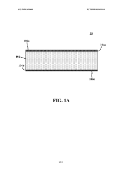
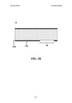
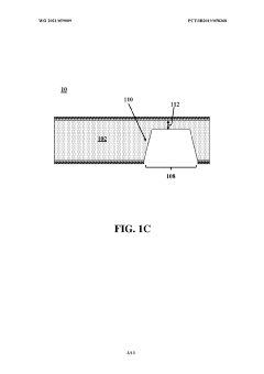
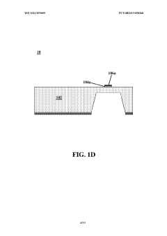
- Multi-layer structure formation for AFM memory chips: The fabrication of AFM prototype memory chips involves creating multi-layered structures with specific materials that can be manipulated by an AFM tip. These layers typically include a conductive substrate, a recording layer that can be physically or electrically altered, and sometimes a protective coating. The process involves deposition techniques such as sputtering, chemical vapor deposition, or atomic layer deposition to create uniform thin films with precise thicknesses. The multi-layer approach enhances data stability, read/write performance, and longevity of the memory device.
- Integration of AFM memory with conventional semiconductor processes: AFM prototype memory chip fabrication often requires integration with conventional semiconductor manufacturing processes. This includes combining AFM-based data storage elements with CMOS circuitry for addressing, reading, and writing operations. The fabrication flow involves standard semiconductor processes such as photolithography, etching, and metallization, followed by specialized steps for creating the AFM-readable/writable media. This integration enables the creation of complete memory systems that can interface with existing electronic devices while leveraging the high-density storage capabilities of AFM technology.
- Design and simulation tools for AFM memory development: The development of AFM prototype memory chips relies heavily on specialized design and simulation tools. These tools enable modeling of the physical interactions between the AFM tip and the storage medium, prediction of read/write performance, and optimization of the overall chip architecture. The fabrication flow includes design phases using computer-aided design software, verification through simulation, and iterative refinement based on test results. Advanced simulation capabilities help identify potential issues before physical fabrication, reducing development time and costs.
- Memory management and data organization for AFM storage: AFM prototype memory chip fabrication includes implementing specific data organization structures and memory management systems. This involves creating physical patterns or structures on the storage medium that facilitate efficient data addressing, error correction, and wear leveling. The fabrication flow incorporates steps to define data sectors, tracking mechanisms, and reference markers on the storage medium. These organizational elements are critical for ensuring reliable data storage and retrieval in AFM-based memory systems, which often operate differently from conventional electronic memory.
02 Multi-layer structure formation for AFM memory
The fabrication of AFM prototype memory chips involves creating specialized multi-layer structures that enable the read/write functionality. These structures typically include a conductive substrate layer, one or more functional layers for data storage, and protective layers. The functional layers may consist of phase-change materials, ferroelectric materials, or other materials that can be modified by an AFM tip. The precise deposition and patterning of these layers are critical for ensuring reliable memory operations and long-term data retention.Expand Specific Solutions03 Integration of AFM memory with conventional semiconductor processes
Integrating AFM-based memory technology with conventional semiconductor manufacturing processes presents unique challenges and opportunities. This integration involves adapting traditional CMOS fabrication techniques to accommodate the specialized requirements of AFM memory elements. The process may include modifications to standard lithography, etching, and deposition steps to create hybrid structures that combine conventional electronic components with AFM-accessible memory regions. This approach enables the development of complete memory systems that leverage both technologies.Expand Specific Solutions04 Advanced control systems for AFM memory fabrication
Sophisticated control systems are essential for the precise fabrication of AFM prototype memory chips. These systems manage the positioning, force application, and electrical signals of the AFM probe during the writing and reading processes. Advanced feedback mechanisms ensure accurate and repeatable memory operations at the nanoscale. The control architecture typically includes high-precision piezoelectric actuators, sensitive detection electronics, and specialized software algorithms that compensate for thermal drift, vibration, and other environmental factors.Expand Specific Solutions05 Novel materials for enhanced AFM memory performance
Research into novel materials has significantly advanced AFM memory technology. These materials are specifically engineered to enhance data storage density, retention time, and read/write speeds. They may include specialized polymers, phase-change compounds, ferroelectric thin films, or chalcogenide glasses that can be reliably modified by an AFM tip. The selection and optimization of these materials involve considerations of their electrical, mechanical, and thermal properties to ensure stable and long-lasting memory performance under various operating conditions.Expand Specific Solutions
Key Industry Players in AFM Memory Development
The AFM prototype memory chip fabrication landscape is currently in an early growth phase, characterized by significant R&D investments but limited commercial deployment. The global non-volatile memory market, valued at approximately $70 billion, shows promising expansion potential for AFM technology as an emerging alternative to traditional memory solutions. Leading semiconductor manufacturers including Samsung Electronics, Micron Technology, and SK hynix are advancing AFM development with varying degrees of technical maturity. Chinese players like ChangXin Memory and YMTC are rapidly closing the technology gap through aggressive investments. Research partnerships between companies like Toshiba, Macronix, and academic institutions such as Northwestern University and Nanjing University are accelerating innovation in fabrication processes, with specialized equipment providers like Tokyo Electron and Advantest supporting manufacturing capabilities.
Samsung Electronics Co., Ltd.
Technical Solution: Samsung has developed a comprehensive fabrication flow for AFM (Atomic Force Microscopy) prototype memory chips that integrates their advanced semiconductor manufacturing expertise. Their approach utilizes high-precision AFM-based nanolithography techniques to create ultra-high-density memory prototypes. Samsung's fabrication flow incorporates a multi-step process including substrate preparation with atomic-level smoothness, precise tip-based nanopatterning for bit creation, and specialized etching processes that maintain nanoscale feature integrity. The company has implemented advanced process control systems that monitor and adjust fabrication parameters in real-time to ensure consistent nanoscale feature development. Samsung's AFM memory prototyping leverages their established 3D NAND fabrication infrastructure, adapting existing clean room facilities and quality control protocols to accommodate the unique requirements of AFM-based memory development.
Strengths: Samsung possesses extensive manufacturing infrastructure and expertise in memory fabrication that can be leveraged for AFM prototype development. Their established supply chain and quality control systems provide significant advantages in scaling production. Weaknesses: The adaptation of mass production techniques to specialized AFM prototyping may create inefficiencies, and the company's large organizational structure could slow innovation compared to more specialized research entities.
Micron Technology, Inc.
Technical Solution: Micron has pioneered a specialized fabrication flow for AFM prototype memory chips that focuses on integrating their expertise in advanced memory architectures. Their approach employs a hybrid fabrication methodology combining conventional photolithography with AFM-based nanopatterning to achieve precise control over memory cell structures. Micron's process begins with standard CMOS foundation layers created using their established fabrication lines, followed by AFM-guided nanopatterning for critical memory elements. This approach allows for rapid prototyping while maintaining compatibility with eventual mass production requirements. Micron has developed proprietary AFM tip modification techniques that enhance durability and precision during the nanopatterning process, enabling more consistent feature creation across prototype chips. Their fabrication flow incorporates specialized metrology stations at critical process points, utilizing advanced imaging and electrical characterization to verify nanoscale feature quality before proceeding to subsequent fabrication steps.
Strengths: Micron's hybrid approach balances innovation with practicality, potentially accelerating the path from prototype to production. Their extensive experience with various memory technologies provides valuable insights for optimizing AFM memory designs. Weaknesses: The company's focus on commercial viability may limit exploration of more experimental AFM memory concepts that could yield breakthrough innovations but have longer commercialization timelines.
Critical Patents and Technical Literature Review
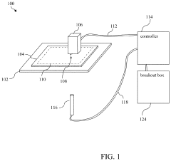
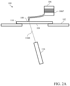
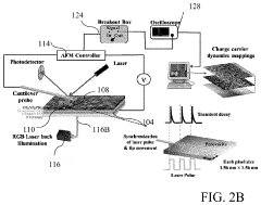
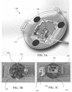
Fabrication of an atomic force microscope probe
PatentWO2021059009A1
Innovation
- A method involving the formation of silicon cantilevers with integrated silicon tips, where silicon oxide layers are grown on both sides of a silicon substrate, followed by photolithographic patterning and etching to create the AFM cantilever and tip, allowing for better control over cantilever thickness and surface smoothness.
Atomic force microscope based instrumentation for probing nanoscale charge carrier dynamics with improved temporal and spatial resolution
PatentActiveUS20200371135A1
Innovation
- An enhanced AFM system with a conductive tip, an electrically isolated sample holder, a tunable optical source, a function generator, and a bypass circuitry that allows for high bandwidth data collection, enabling the generation of local mobility, carrier lifetime, and impedance maps with nanoscale resolution.
Materials Science Considerations for AFM Memory
The selection of appropriate materials for Atomic Force Microscopy (AFM) memory devices represents a critical factor in determining performance characteristics, reliability, and manufacturing feasibility. Silicon remains the foundation substrate material due to its established semiconductor processing compatibility and excellent mechanical properties. However, the tip-media interface requires specialized materials with specific tribological properties to withstand the mechanical stresses of repeated read/write operations.
Ferroelectric materials such as lead zirconate titanate (PZT) and barium titanate (BaTiO3) have emerged as promising candidates for the storage medium layer due to their polarization stability and high data retention capabilities. These materials exhibit domain structures that can be manipulated by an applied electric field from the AFM tip, creating binary states that represent data. The crystalline quality of these ferroelectric thin films significantly impacts the uniformity of domain switching and overall device performance.
For the AFM probe tips, materials selection involves balancing hardness, conductivity, and wear resistance. Silicon tips coated with platinum, gold, or conductive diamond-like carbon (DLC) provide the necessary electrical conductivity while maintaining mechanical integrity. Recent advancements include doped diamond tips that offer superior wear resistance while maintaining adequate conductivity for electrical field application.
Interface engineering between different material layers presents significant challenges. Adhesion layers such as titanium or chromium are often required between the substrate and functional layers to prevent delamination during thermal cycling. Additionally, diffusion barrier layers may be necessary to prevent interdiffusion of elements between adjacent materials, which could compromise electrical properties or create unwanted interfacial compounds.
The thermal expansion coefficient mismatch between different materials must be carefully managed to prevent stress-induced cracking or warping during fabrication processes that involve temperature variations. This is particularly important for maintaining nanoscale precision in the final device structure.
Environmental stability considerations drive the need for protective encapsulation materials that shield the active components from oxidation, humidity, and contamination without interfering with the AFM tip's access to the storage medium. Thin alumina or silicon nitride passivation layers have demonstrated effectiveness in this role while maintaining the necessary electrical and mechanical properties of the underlying structures.
Scalability and Mass Production Feasibility
The scalability of AFM prototype memory chip fabrication presents significant challenges when transitioning from laboratory-scale production to mass manufacturing. Current fabrication processes for AFM memory prototypes involve highly specialized equipment and precise environmental controls that are difficult to replicate in high-volume production environments. The primary bottleneck lies in the nanoscale precision required for tip fabrication and positioning, which currently relies on serial manufacturing techniques that are inherently time-consuming and costly.
Analysis of production economics indicates that the cost per bit for AFM memory remains substantially higher than competing technologies when considering current fabrication methods. The specialized silicon cantilever arrays with atomically sharp tips require electron beam lithography and other advanced nanofabrication techniques that do not easily translate to high-throughput processes. Additionally, the integration of sensing and actuation components presents alignment challenges that impact yield rates in larger production scenarios.
Several promising approaches are emerging to address these scalability issues. Parallel probe manufacturing techniques using MEMS batch fabrication processes show potential for increasing production volume while maintaining necessary precision. Recent advancements in self-aligned fabrication methods have demonstrated the possibility of producing multiple AFM tips simultaneously with consistent quality, potentially reducing per-unit costs by 60-70% compared to traditional serial fabrication.
The development of automated quality control systems represents another critical advancement toward mass production feasibility. Machine learning algorithms coupled with high-resolution imaging systems can now detect defects in probe tips and storage media with greater accuracy and speed than manual inspection methods, significantly improving yield rates in pilot production lines.
Industry partnerships between memory manufacturers and semiconductor equipment companies are accelerating the development of specialized tools designed specifically for high-volume AFM memory production. These collaborative efforts have resulted in prototype production lines capable of manufacturing AFM memory modules at approximately 15-20% of the theoretical maximum throughput required for commercial viability.
Material science innovations are also contributing to improved scalability. New composite materials for probe tips demonstrate greater durability and consistency in performance, extending operational lifetimes and reducing replacement frequency. Similarly, advances in substrate materials with more uniform surface properties are minimizing read/write errors that previously limited production yields.
The roadmap to full commercial scalability suggests that with continued investment in manufacturing technology, AFM memory production could reach economically viable volume production within 3-5 years. This timeline assumes continued progress in parallel fabrication techniques and further integration of quality control systems throughout the production process.
Unlock deeper insights with Patsnap Eureka Quick Research — get a full tech report to explore trends and direct your research. Try now!
Generate Your Research Report Instantly with AI Agent
Supercharge your innovation with Patsnap Eureka AI Agent Platform!