

Cryogenic Electronics: Electrode Kinetics at Low Temperatures
SEP 29, 202510 MIN READ
Generate Your Research Report Instantly with AI Agent
PatSnap Eureka helps you evaluate technical feasibility & market potential.
Cryogenic Electronics Background and Objectives
Cryogenic electronics represents a frontier field at the intersection of electrical engineering, materials science, and quantum physics. The study of electrode kinetics at low temperatures has evolved significantly since the mid-20th century, when researchers first began exploring the behavior of electronic components in extreme cold environments. Initially driven by space exploration needs and fundamental physics research, this field has expanded dramatically with the advent of quantum computing, superconducting technologies, and advanced sensing applications.
The evolution of cryogenic electronics has been marked by several key technological breakthroughs, including the development of specialized semiconductor materials that maintain functionality at temperatures approaching absolute zero, novel electrode designs that minimize thermal noise, and superconducting circuits that exhibit zero electrical resistance. These advancements have collectively pushed the boundaries of what's possible in electronic performance, energy efficiency, and quantum coherence.
Current trends in the field point toward miniaturization of cryogenic systems, integration with room-temperature electronics, and development of materials with optimized electrode kinetics at varying temperature ranges. The emergence of quantum information processing has particularly accelerated research in this domain, as quantum bits (qubits) typically require operation at millikelvin temperatures to maintain quantum coherence and minimize decoherence effects.
The primary technical objectives in cryogenic electrode kinetics research include understanding and controlling charge transfer mechanisms at interfaces under extreme cold conditions, developing electrodes with enhanced stability and performance at cryogenic temperatures, and creating comprehensive models that accurately predict electronic behavior across wide temperature ranges. These objectives serve both fundamental science and practical applications.
Beyond quantum computing, cryogenic electronics aims to enable ultra-sensitive detectors for astronomy and particle physics, advance medical imaging technologies through superconducting sensors, and support next-generation space exploration with electronics capable of functioning in the extreme cold of deep space. The field also seeks to develop energy-efficient computing architectures that leverage superconductivity to minimize power consumption.
Achieving these objectives requires overcoming significant challenges in materials compatibility, thermal management, and signal integrity. Researchers must develop electrodes that maintain consistent kinetic properties despite thermal cycling, design interfaces that minimize parasitic effects at low temperatures, and create packaging solutions that effectively isolate sensitive components from environmental influences.
The convergence of these research directions positions cryogenic electrode kinetics as a critical enabling technology for next-generation computing, sensing, and communication systems, with potential impacts spanning multiple industries and scientific disciplines.
Market Applications for Low-Temperature Electronic Systems
The market for cryogenic electronics is experiencing significant growth, driven by advancements in quantum computing, space exploration, and medical imaging technologies. The global quantum computing market alone is projected to reach $1.7 billion by 2026, with a substantial portion requiring cryogenic electronic systems to function optimally. These low-temperature electronic systems are essential for maintaining quantum coherence in quantum bits (qubits), which typically operate at temperatures approaching absolute zero.
In the healthcare sector, superconducting quantum interference devices (SQUIDs) used in magnetoencephalography (MEG) and magnetic resonance imaging (MRI) systems represent a mature market for cryogenic electronics. The medical imaging equipment market, valued at approximately $32 billion globally, continues to drive demand for more sensitive and efficient cryogenic components that can operate reliably at liquid helium temperatures (4.2K).
Space exploration and satellite communications present another substantial market opportunity. Cryogenic electronics enable higher sensitivity in deep-space communication receivers and astronomical instruments. NASA, ESA, and emerging private space companies are investing heavily in cryogenic technologies to enhance the performance of space-based observatories and long-distance communication systems.
The semiconductor testing industry also relies on cryogenic electronics for wafer-level testing at extremely low temperatures. This market segment is expected to grow as semiconductor manufacturers push toward smaller process nodes where quantum effects become increasingly significant. The ability to characterize devices at cryogenic temperatures provides valuable insights into performance parameters that cannot be observed at room temperature.
Defense and security applications represent a specialized but high-value market for cryogenic electronics. Superconducting digital electronics offer unprecedented speed and energy efficiency for signal processing in radar systems and secure communications. Military research agencies continue to fund development of cryogenic computing architectures that could potentially overcome the limitations of conventional semiconductor technologies.
Emerging applications in quantum sensing and metrology are creating new market opportunities. Superconducting sensors operating at cryogenic temperatures can achieve unprecedented sensitivity for measuring magnetic fields, gravitational waves, and other physical phenomena. These instruments are finding applications in geophysical exploration, fundamental physics research, and next-generation navigation systems that don't rely on GPS.
The industrial cryogenics market, which provides the cooling infrastructure necessary for these applications, is projected to grow at a compound annual rate of 7.2% through 2028, reflecting the expanding demand for low-temperature electronic systems across multiple sectors.
Current Challenges in Electrode Kinetics at Cryogenic Temperatures
The field of cryogenic electronics faces significant challenges in understanding and controlling electrode kinetics at extremely low temperatures. As temperatures approach absolute zero, conventional models of electron transfer and electrochemical reactions break down, creating fundamental scientific hurdles. The standard Butler-Volmer equation, which adequately describes electrode kinetics at room temperature, fails to account for quantum effects that become dominant in cryogenic environments.
One major challenge is the dramatic decrease in reaction rates at cryogenic temperatures. The Arrhenius relationship predicts exponentially slower kinetics as temperature decreases, but experimental evidence shows deviations from this model below approximately 50K. This discrepancy points to quantum tunneling mechanisms becoming increasingly important, yet quantitative models incorporating these effects remain incomplete.
Material constraints present another significant obstacle. Electrode materials that perform well at room temperature often exhibit drastically different properties at cryogenic temperatures. Thermal contraction can create mechanical stress and potential delamination at electrode interfaces. Additionally, the electrical conductivity of many materials changes non-linearly at low temperatures, complicating the design of reliable electrode systems.
The formation and behavior of the electrical double layer—crucial for understanding electrode kinetics—undergoes fundamental changes at cryogenic temperatures. Reduced thermal motion alters ion distribution near electrode surfaces, while solvent properties change dramatically. Many conventional electrolytes freeze or become highly viscous, severely limiting ion mobility and changing the nature of charge transfer processes.
Measurement techniques themselves introduce significant challenges. Conventional electrochemical methods require adaptation for cryogenic environments, with issues including thermal gradients, reduced signal-to-noise ratios, and difficulties in reference electrode stability. The integration of cryostats with electrochemical cells introduces design complexities that can compromise measurement accuracy.
Theoretical frameworks for cryogenic electrode kinetics remain underdeveloped. While quantum mechanical approaches offer promising avenues, they typically require significant computational resources and often lack experimental validation. The interplay between quantum effects, reduced thermal energy, and altered material properties creates a complex system that defies simple modeling approaches.
Perhaps most challenging is the limited cross-disciplinary collaboration between cryogenic engineering, quantum physics, and electrochemistry. Advances in this field require expertise spanning multiple domains, yet traditional academic and industrial boundaries have historically limited such interdisciplinary work. This organizational challenge compounds the technical difficulties, slowing progress toward comprehensive understanding of electrode kinetics at cryogenic temperatures.
State-of-the-Art Solutions for Low-Temperature Electrode Performance
01 Cryogenic electrode materials and structures
Specialized electrode materials and structures designed for operation at cryogenic temperatures are essential for maintaining electrical performance in extreme cold environments. These electrodes incorporate materials with stable conductivity at low temperatures and specific structural designs that accommodate thermal contraction. Advanced fabrication techniques ensure proper electrode-substrate interfaces that maintain integrity during temperature cycling, which is critical for reliable operation of cryogenic electronic systems.- Cryogenic electrode materials and structures: Specialized electrode materials and structures designed for operation at cryogenic temperatures, featuring enhanced conductivity and stability under extreme cold conditions. These electrodes incorporate novel compositions and geometries that maintain electrical performance while minimizing thermal expansion issues. The designs address challenges of electron mobility and charge transfer kinetics at ultra-low temperatures, enabling reliable electronic functionality in cryogenic environments.
- Superconducting quantum electronics: Quantum electronic systems operating at cryogenic temperatures that leverage superconducting properties for enhanced performance. These systems utilize electrode configurations specifically designed for quantum bit (qubit) operations, featuring precise control of electron behavior at the quantum level. The electrode kinetics in these systems are optimized to maintain quantum coherence while facilitating measurement and control operations in superconducting circuits.
- Cryogenic cooling systems for electronics: Specialized cooling systems designed to maintain electronic components at cryogenic temperatures while ensuring proper electrode functionality. These systems incorporate advanced thermal management techniques to create stable temperature environments for sensitive electronic operations. The designs address challenges of thermal gradients, cooling efficiency, and mechanical stress on electrode structures during rapid temperature transitions.
- Low-temperature electron transport mechanisms: Fundamental mechanisms governing electron transport and electrode kinetics at cryogenic temperatures, including quantum tunneling effects and modified charge carrier behavior. These mechanisms influence how electrons move through materials and across interfaces when thermal energy is minimized. Understanding these transport phenomena enables the design of electrode systems that maintain functionality despite the significant changes in electron behavior that occur at extremely low temperatures.
- Cryogenic measurement and sensing electrodes: Specialized electrode designs for measurement, sensing, and characterization applications in cryogenic environments. These electrodes feature enhanced sensitivity and signal-to-noise ratios at extremely low temperatures, enabling precise measurements of electrical, magnetic, and quantum properties. The designs incorporate materials and geometries that minimize thermal noise and maintain stable reference potentials, allowing for accurate data collection in scientific and industrial cryogenic applications.
02 Electron transport mechanisms at cryogenic temperatures
The kinetics of electron transport in cryogenic environments differs significantly from room temperature behavior. At extremely low temperatures, quantum effects become dominant, and conventional electron flow models must be modified. Research focuses on understanding and controlling these transport mechanisms, including superconducting phenomena, tunneling effects, and ballistic transport. These mechanisms are fundamental to developing high-performance cryogenic electronic components with improved signal processing capabilities.Expand Specific Solutions03 Cryogenic cooling systems for electronic applications
Specialized cooling systems are required to maintain stable cryogenic temperatures for electronic components. These systems include various refrigeration technologies such as Joule-Thomson coolers, pulse tube refrigerators, and dilution refrigerators. The design focuses on minimizing thermal gradients, reducing vibration, and ensuring long-term operational stability. Efficient thermal management is critical for maintaining electrode performance and extending the operational lifetime of cryogenic electronic systems.Expand Specific Solutions04 Interface phenomena between electrodes and cryogenic environments
The interface between electrodes and their cryogenic environment presents unique challenges related to charge transfer kinetics. These interfaces experience phenomena such as charge trapping, altered surface chemistry, and modified energy barriers. Understanding these interface effects is crucial for designing electrodes that maintain efficient charge transfer at extremely low temperatures. Research in this area focuses on surface treatments, interface engineering, and novel material combinations to optimize electrode performance.Expand Specific Solutions05 Measurement and characterization techniques for cryogenic electrodes
Specialized measurement techniques are required to accurately characterize electrode performance at cryogenic temperatures. These include impedance spectroscopy, cyclic voltammetry at low temperatures, and quantum transport measurements. Advanced instrumentation has been developed to isolate measurement signals from thermal noise and to maintain sample temperature stability during testing. These techniques are essential for understanding electrode kinetics and for validating theoretical models of charge transfer in extreme cold environments.Expand Specific Solutions
Leading Research Institutions and Companies in Cryogenic Electronics
Cryogenic Electronics: Electrode Kinetics at Low Temperatures is currently in an early growth phase, with the market expected to expand significantly due to increasing applications in quantum computing and superconducting technologies. The global market size is projected to reach approximately $2-3 billion by 2025, driven by research advancements and commercial applications. Leading players like IBM, PsiQuantum, and Equal1 Laboratories are pioneering quantum computing solutions utilizing cryogenic electronics, while research institutions such as VTT, Naval Research Laboratory, and University of Maryland are advancing fundamental understanding of electrode behavior at ultra-low temperatures. The technology remains in development stage with significant R&D investment from both private companies and government entities, indicating strong future growth potential as quantum technologies mature.
International Business Machines Corp.
Technical Solution: IBM has pioneered significant advancements in cryogenic electronics, particularly focusing on electrode kinetics at low temperatures for quantum computing applications. Their approach involves superconducting qubits operating at millikelvin temperatures (typically 10-20 mK), where they've developed specialized Josephson junction electrodes with precisely controlled tunnel barriers. IBM's research has yielded breakthroughs in materials science for these electrodes, using aluminum-aluminum oxide-aluminum structures that maintain quantum coherence at ultra-low temperatures. Their cryogenic control electronics integrate both semiconductor and superconducting components to minimize thermal load while maximizing signal integrity. Recent developments include their "Quantum System One" architecture that incorporates advanced cryogenic wiring solutions and custom-designed dilution refrigerators to maintain stable electrode performance across temperature gradients from room temperature to millikelvin environments.
Strengths: IBM possesses unparalleled integration capabilities between quantum processing units and classical control electronics, with demonstrated coherence times exceeding 100 microseconds in their latest designs. Their global research infrastructure enables rapid iteration and testing of new electrode materials and configurations. Weaknesses: Their solutions require extremely expensive cooling infrastructure and face challenges in scaling up the number of qubits while maintaining low error rates due to thermal management issues.
Semiqon Technologies Oy
Technical Solution: Semiqon Technologies has developed specialized cryogenic electrode systems focusing on semiconductor-superconductor interfaces for quantum information processing. Their proprietary approach involves epitaxially grown semiconductor nanowires with precisely engineered superconducting contacts that maintain optimal electrode kinetics at sub-Kelvin temperatures. The company has pioneered techniques for minimizing the Schottky barrier formation at these interfaces, which typically degrades at cryogenic temperatures due to carrier freeze-out effects. Their technology incorporates in-situ surface preparation methods before metallization to ensure atomically clean interfaces, followed by carefully controlled deposition of superconducting materials (primarily aluminum and niobium-based alloys) to create transparent electrical contacts. Semiqon's cryogenic measurement systems include custom-designed filtering solutions that minimize electromagnetic interference while allowing precise characterization of quantum devices at millikelvin temperatures, enabling detailed studies of electrode kinetics in these extreme conditions.
Strengths: Semiqon excels in creating high-transparency superconductor-semiconductor interfaces with minimal contact resistance at cryogenic temperatures, crucial for quantum device performance. Their specialized knowledge of surface chemistry at low temperatures gives them unique capabilities in electrode engineering. Weaknesses: As a smaller company, they have limited manufacturing scale compared to larger competitors, and their solutions may be less integrated into complete quantum computing systems.
Key Patents and Research Breakthroughs in Cryogenic Electrode Kinetics
Cryogenic packaging for thermalization of low temperature devices
PatentWO2020254596A1
Innovation
- A cryogenic packaging system featuring a cover with pillars and cavities on the chip, allowing for thermal coupling without reducing chip thickness, using materials like copper and depositing thermal conductive linings to enhance heat dissipation, maintaining chip rigidity and alignment.


Interfacing at low temperature using CMOS technology
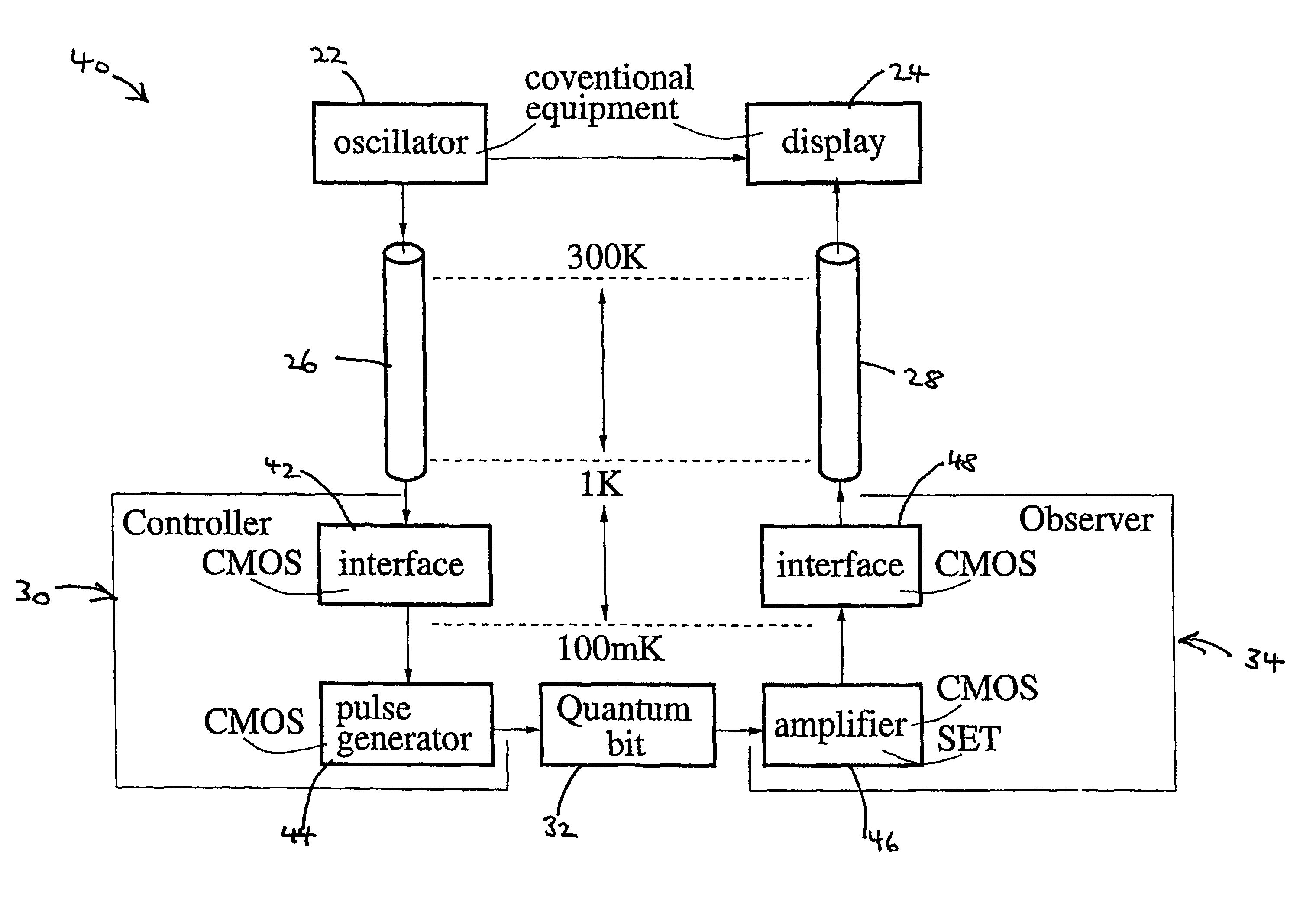
PatentActiveUS7911265B2
Innovation
- The development of ultra-thin silicon-on-insulator (SOI) CMOS technology for fabricating controller and observer circuits, which utilize SOI-CMOSFETs to achieve high unity-gain frequency, rapid pulse edge transition times, high bandwidth, and low power operation, enabling effective control and measurement of quantum bits at low temperatures.
Materials Science Advancements for Cryogenic Applications
The evolution of cryogenic electronics has been significantly influenced by advancements in materials science. Traditional electronic materials often exhibit drastically altered properties at extremely low temperatures, necessitating specialized materials development. Recent breakthroughs in superconducting materials have enabled more efficient operation of cryogenic electronic systems, with critical temperature thresholds being gradually increased through novel material compositions and fabrication techniques.
Electrode materials for cryogenic applications have seen remarkable innovation, particularly in the development of composite structures that maintain conductivity while minimizing thermal expansion mismatches. These materials incorporate nanoscale engineering to preserve electrode kinetics at temperatures approaching absolute zero, where conventional electron transport mechanisms become highly constrained.
Thin-film deposition technologies have revolutionized cryogenic electrode fabrication, allowing for precise control of material interfaces critical to maintaining electrode kinetics. Advanced techniques such as atomic layer deposition and molecular beam epitaxy enable the creation of atomically precise structures that optimize electron transfer processes even under extreme temperature conditions.
Substrate materials have also undergone significant evolution, with silicon carbide, sapphire, and specialized ceramics emerging as preferred platforms for cryogenic electronic circuits. These materials provide the necessary thermal stability while maintaining compatible coefficients of thermal expansion with active electronic components, preventing mechanical failures during thermal cycling.
Novel insulating materials with enhanced dielectric properties at low temperatures have addressed the challenge of maintaining signal integrity in cryogenic environments. These materials exhibit minimal dielectric losses and stable capacitive characteristics, enabling precise control of electrode kinetics in sensing and computing applications.
Surface modification techniques have emerged as a critical area of research, with functionalized electrode surfaces demonstrating improved electron transfer rates at cryogenic temperatures. These modifications often involve nanoscale texturing and chemical treatments that optimize the electrode-electrolyte interface, maintaining reaction kinetics that would otherwise be severely limited by thermal constraints.
Quantum materials represent the frontier of cryogenic electronics research, with two-dimensional materials like graphene and transition metal dichalcogenides showing unique electronic properties at low temperatures. These materials exhibit quantum confinement effects that can be harnessed for novel electrode designs, potentially enabling entirely new paradigms in cryogenic electronic systems and quantum computing architectures.
Quantum Computing Integration and Opportunities
The integration of cryogenic electronics with quantum computing represents a transformative frontier in computational technology. Quantum computers fundamentally rely on maintaining quantum coherence, which is typically achieved at extremely low temperatures where thermal noise is minimized. The electrode kinetics at these cryogenic temperatures directly impacts the performance, reliability, and scalability of quantum computing systems.
Current quantum computing architectures, particularly those based on superconducting qubits, operate at millikelvin temperatures. At these temperatures, conventional electronic components often fail or exhibit significantly altered behaviors. The development of specialized cryogenic electronics that can function reliably at these extreme conditions is therefore critical for quantum computing advancement.
Several major technology companies and research institutions have begun integrating cryogenic electronic systems with quantum processors. Intel's Horse Ridge cryogenic control chip represents a significant milestone, enabling control signal generation at temperatures closer to the quantum processor, thereby reducing signal degradation and improving qubit control precision. Similarly, Google's Sycamore processor incorporates specialized cryogenic interconnects to maintain quantum coherence while facilitating necessary electronic control.
The opportunities emerging from this integration are substantial. First, improved electrode kinetics at low temperatures could significantly enhance qubit fidelity and coherence times, addressing one of the fundamental challenges in quantum computing. Second, cryogenic electronics enable more efficient scaling of quantum systems by allowing control electronics to be positioned closer to quantum processors, reducing wiring complexity and associated thermal loads.
Furthermore, advances in cryogenic electrode materials and designs could lead to novel quantum computing architectures. Superconducting materials with optimized electrode kinetics at low temperatures may enable new types of quantum gates with higher fidelity and lower error rates. The development of cryogenic CMOS technologies also presents opportunities for creating integrated quantum-classical computing systems, where classical processing occurs in close proximity to quantum operations.
The economic implications are equally significant. As quantum computing transitions from research to commercial applications, the market for specialized cryogenic electronic components is expected to grow substantially. Companies that develop expertise in cryogenic electrode technologies may secure advantageous positions in the quantum computing supply chain.
Looking forward, the convergence of cryogenic electronics and quantum computing will likely accelerate as both fields mature. Innovations in electrode materials, interface engineering, and cryogenic circuit design will continue to push the boundaries of what's possible in quantum information processing, potentially enabling practical quantum advantage across multiple industries.
Unlock deeper insights with PatSnap Eureka Quick Research — get a full tech report to explore trends and direct your research. Try now!
Generate Your Research Report Instantly with AI Agent
Supercharge your innovation with PatSnap Eureka AI Agent Platform!