

Designing Peripheral Circuits For AFM Memory Arrays
SEP 1, 20259 MIN READ
Generate Your Research Report Instantly with AI Agent
PatSnap Eureka helps you evaluate technical feasibility & market potential.
AFM Memory Technology Background and Objectives
Antiferromagnetic (AFM) memory technology represents a significant evolution in the field of non-volatile memory systems, emerging as a promising alternative to conventional magnetic storage technologies. The development of AFM memory can be traced back to the early 2010s when researchers began exploring antiferromagnetic materials for spintronics applications. Unlike ferromagnetic materials used in traditional magnetic storage, antiferromagnetic materials exhibit no net magnetic moment, making them inherently stable against external magnetic field disturbances.
The technological evolution of AFM memory has been driven by increasing demands for higher density, faster operation, and lower power consumption in memory systems. Traditional memory technologies face fundamental physical limitations as dimensions shrink below certain thresholds. AFM memory offers potential solutions to these challenges through its unique physical properties, including terahertz operating frequencies, immunity to external magnetic fields, and zero stray fields that allow for higher integration density.
The primary objective of AFM memory technology development is to create commercially viable memory arrays that can compete with or surpass existing technologies in terms of performance metrics. This includes achieving write speeds in the sub-nanosecond range, read reliability with sufficient signal-to-noise ratio, and endurance cycles exceeding 10^12 operations while maintaining data retention periods of over 10 years at operating temperatures.
Current research focuses on overcoming several key challenges, particularly in the realm of peripheral circuit design. These circuits must be capable of generating and precisely controlling the electrical currents required for writing operations, as well as detecting the small resistance changes during reading operations. The peripheral circuits represent a critical component in translating the theoretical advantages of AFM materials into practical memory devices.
The technology aims to position itself in various market segments, from embedded memory applications to standalone storage solutions. In particular, AFM memory shows promise for applications requiring radiation hardness, such as aerospace and military systems, as well as for ultra-low power applications in IoT devices and wearable technology.
Recent breakthroughs in materials science, particularly in the development of CuMnAs and Mn2Au thin films, have accelerated progress in this field. These materials exhibit the necessary properties for electrical manipulation of the Néel vector, which is essential for electrical writing operations in AFM memory cells. Additionally, advances in fabrication techniques have enabled the creation of nanoscale AFM structures compatible with CMOS processes.
The ultimate technological goal is to develop a fully integrated AFM memory array with peripheral circuits that can be manufactured using standard semiconductor processes, offering a competitive alternative to existing memory technologies while opening new application possibilities through its unique characteristics.
Market Analysis for AFM Memory Solutions
The global market for Anti-Ferromagnetic (AFM) memory solutions is experiencing significant growth, driven by increasing demand for high-performance, energy-efficient, and radiation-hardened memory technologies. Current market projections indicate that the emerging non-volatile memory market, which includes AFM memory, is expected to reach $13.7 billion by 2025, with a compound annual growth rate of 38.3% from 2020.
AFM memory solutions are positioned to address critical limitations in existing memory technologies. Traditional DRAM faces scalability challenges below 10nm nodes and suffers from high power consumption due to refresh requirements. NAND Flash, while dominant in the storage market, struggles with endurance limitations and slow write speeds. These shortcomings create substantial market opportunities for AFM memory, particularly in applications requiring both high performance and non-volatility.
The enterprise storage sector represents the largest potential market for AFM memory solutions, as data centers increasingly demand faster, more reliable storage systems with lower power consumption. Market research indicates that data center operators could reduce operational costs by up to 30% through the adoption of energy-efficient memory technologies like AFM memory.
Mobile and IoT devices constitute another rapidly growing market segment. With over 25 billion connected devices projected by 2025, the demand for low-power, high-density memory solutions is escalating. AFM memory's potential for ultra-low standby power consumption makes it particularly attractive for battery-powered devices, potentially extending operational life by 40-60% compared to current solutions.
The automotive sector presents a specialized but lucrative market opportunity. Advanced driver-assistance systems and autonomous vehicles require radiation-hardened, temperature-resistant memory that can operate reliably in harsh environments. This segment is projected to grow at 45% annually through 2025, creating premium pricing opportunities for specialized memory solutions.
Aerospace and defense applications form a smaller but high-margin market segment. These applications demand radiation-hardened memory solutions that can withstand extreme conditions, with procurement contracts often valuing reliability and performance over cost considerations.
Geographically, North America currently leads in AFM memory technology adoption, accounting for approximately 42% of the market share, followed by Asia-Pacific at 35% and Europe at 18%. However, the Asia-Pacific region is expected to demonstrate the fastest growth rate over the next five years due to increasing semiconductor manufacturing capabilities and rising demand for advanced electronic devices.
Customer adoption barriers include integration challenges with existing systems, concerns about long-term reliability, and price premiums compared to established technologies. Market analysis suggests that achieving price parity with conventional memory solutions will be crucial for widespread adoption, with industry experts predicting this crossover point could occur within 4-6 years as manufacturing processes mature.
Current Peripheral Circuit Challenges
The peripheral circuits surrounding AFM (Atomic Force Microscopy) memory arrays face significant challenges that impede the widespread adoption of this promising storage technology. One of the primary obstacles is the integration complexity between the nanoscale AFM tips and conventional CMOS circuitry. The dimensional mismatch creates interconnection difficulties, requiring sophisticated interface solutions that add to manufacturing complexity and cost.
Signal integrity represents another critical challenge, as the read signals from AFM memory cells are inherently weak, typically in the nanoampere or even picoampere range. This necessitates highly sensitive amplification circuits with exceptional signal-to-noise ratios, which are difficult to design without introducing additional noise or distortion that could compromise data reliability.
Power consumption concerns are particularly acute in peripheral circuits for AFM memory arrays. The mechanical movement of AFM tips requires precise control circuitry that traditionally consumes significant power. This becomes especially problematic for portable or IoT applications where energy efficiency is paramount. Current designs struggle to balance the need for precise mechanical control with reasonable power budgets.
Speed limitations present another substantial hurdle. The mechanical nature of AFM tip movement inherently restricts operational speed compared to purely electronic memory technologies. Peripheral circuits must compensate for this mechanical latency while maintaining data integrity, creating a complex design trade-off between speed, accuracy, and power consumption.
Addressing schemes for large AFM memory arrays introduce additional complexity. As array sizes increase, the peripheral circuits must manage increasingly complex addressing protocols while maintaining acceptable access times. Current solutions often struggle to scale efficiently beyond certain array dimensions, limiting the practical density advantages of AFM memory.
Reliability and wear management represent ongoing challenges for peripheral circuit designers. AFM tips experience mechanical wear over time, requiring sophisticated detection and compensation circuits. Current peripheral designs lack robust, integrated solutions for real-time wear monitoring and adaptive control to extend the operational lifespan of AFM memory arrays.
Temperature sensitivity further complicates peripheral circuit design, as thermal expansion can significantly impact the nanoscale precision required for AFM operation. Compensation circuits must account for these thermal effects without adding excessive complexity or power requirements, a balance that remains difficult to achieve with current technology approaches.
Existing Peripheral Circuit Architectures
01 Sense Amplifier Designs for AFM Memory Arrays
Specialized sense amplifiers are critical peripheral circuits for AFM memory arrays, enabling reliable reading of stored data. These designs include differential sensing techniques to detect small resistance changes in AFM cells, reference cell comparison methods, and current-mode sensing architectures. Advanced sense amplifiers incorporate noise reduction features and temperature compensation to maintain accuracy across operating conditions.- Sense amplifier designs for AFM memory arrays: Specialized sense amplifiers are critical peripheral circuits for AFM (Antiferromagnetic) memory arrays. These circuits are designed to detect and amplify the small resistance changes that occur when reading data from AFM memory cells. Advanced sense amplifier designs incorporate differential sensing techniques, reference cells, and specialized timing circuits to improve read reliability and speed while minimizing power consumption.
- Row and column decoder circuits for AFM memory access: Row and column decoder circuits are essential peripheral components that enable selective access to specific memory cells within AFM memory arrays. These circuits translate memory addresses into physical cell locations by activating the appropriate word lines and bit lines. Advanced decoder designs incorporate hierarchical structures, predecoding techniques, and specialized drivers to optimize access speed while minimizing area overhead and power consumption.
- Write driver circuits for AFM memory arrays: Write driver circuits provide the necessary current or voltage pulses to program AFM memory cells. These specialized peripheral circuits must generate precisely controlled signals with appropriate amplitude, duration, and timing to ensure reliable data storage. Advanced write driver designs incorporate current steering techniques, programmable pulse shaping, and verification mechanisms to accommodate variations in cell characteristics while minimizing write errors.
- Error correction and redundancy circuits: Error correction and redundancy circuits are critical peripheral components that enhance the reliability and yield of AFM memory arrays. These circuits detect and correct bit errors during read operations and can reroute access to redundant memory cells when permanent defects are identified. Advanced implementations include on-chip error correction coding (ECC), built-in self-test (BIST), and repair mechanisms that significantly improve overall memory performance and longevity.
- Power management and control circuits: Power management and control circuits are essential peripheral components that regulate the operation of AFM memory arrays. These circuits generate and distribute various supply voltages, reference signals, and timing clocks required by different memory blocks. Advanced designs incorporate dynamic voltage scaling, selective power gating, and adaptive biasing techniques to optimize performance while minimizing power consumption, particularly important for battery-powered applications.
02 Address Decoders and Row/Column Selection Circuits
Address decoders and row/column selection circuits are essential peripheral components that enable precise access to specific memory cells within AFM arrays. These circuits translate external address inputs into internal row and column selection signals, activating the appropriate word lines and bit lines. Advanced implementations include hierarchical decoding structures to minimize access time and power consumption while maintaining addressing accuracy for high-density arrays.Expand Specific Solutions03 Write Driver Circuits for AFM Memory
Write driver circuits provide the necessary current and voltage signals to program AFM memory cells. These specialized circuits generate precisely controlled pulses with appropriate amplitude and duration to switch the resistance state of the memory elements. Advanced write drivers incorporate current limiting features, voltage regulation, and timing control to ensure reliable programming while preventing damage to the memory cells from excessive current or voltage stress.Expand Specific Solutions04 Error Detection and Correction Circuits
Error detection and correction circuits enhance the reliability of AFM memory arrays by identifying and rectifying data errors. These peripheral circuits implement various error correction code (ECC) algorithms to detect bit errors during read operations and correct them when possible. Advanced implementations include multi-bit error correction capabilities, adaptive correction schemes, and background error scanning to maintain data integrity over the lifetime of the memory.Expand Specific Solutions05 Power Management and Control Circuits
Power management and control circuits optimize the operation of AFM memory arrays by regulating supply voltages, controlling timing sequences, and managing power consumption. These peripheral circuits include voltage regulators, clock generators, and power gating mechanisms that enable different operating modes such as active, standby, and sleep. Advanced implementations feature adaptive power schemes that adjust operating parameters based on workload and temperature to maximize performance while minimizing energy consumption.Expand Specific Solutions
Leading Companies in AFM Memory Development
The AFM memory array peripheral circuit design market is in a growth phase, characterized by increasing demand for high-density, low-power memory solutions. The market is expected to reach significant scale as AFM technology matures, driven by applications in data centers, mobile devices, and automotive systems. From a technical maturity perspective, established semiconductor leaders like Samsung Electronics, Micron Technology, and SK hynix are advancing core AFM technologies, while specialized players such as YMTC and KIOXIA are developing innovative peripheral circuit designs to enhance performance. Companies like TSMC and GlobalFoundries provide critical manufacturing capabilities, while Qualcomm and Texas Instruments contribute expertise in system integration. The competitive landscape features collaboration between memory manufacturers and semiconductor foundries to overcome technical challenges in scaling, power efficiency, and reliability of AFM memory peripheral circuits.
Micron Technology, Inc.
Technical Solution: Micron has developed specialized peripheral circuits for AFM memory arrays that focus on maximizing performance while minimizing area overhead. Their approach utilizes a hierarchical bit-line architecture with local and global sensing to reduce parasitic capacitance and improve read speeds. Micron's peripheral circuit design incorporates advanced current-mode sense amplifiers that provide faster sensing with lower voltage swings, critical for AFM's typically smaller signal margins. Their solution includes adaptive write drivers that can modulate pulse width, amplitude, and shape based on feedback from verification circuits to optimize write operations. Micron has implemented intelligent power management circuits that selectively activate only the necessary peripheral components during different operations, significantly reducing overall power consumption. Additionally, their design includes on-chip temperature sensors and compensation circuits that adjust timing and reference voltages to maintain consistent performance across varying environmental conditions. Micron's peripheral circuits also feature built-in self-test and repair functionality to improve yield and reliability.
Strengths: Excellent power efficiency through intelligent power management, superior read performance through hierarchical sensing architecture, and robust adaptive write schemes. Weaknesses: Potentially higher manufacturing complexity due to the sophisticated sensing circuits, and the adaptive systems may require more silicon area than simpler implementations.
Samsung Electronics Co., Ltd.
Technical Solution: Samsung has developed advanced peripheral circuits for AFM (Anti-Ferroelectric Memory) arrays that integrate with their existing NAND and DRAM technologies. Their approach focuses on high-density integration using 3D stacking architecture with specialized sense amplifiers capable of detecting the small polarization signals characteristic of AFM cells. Samsung's peripheral circuit design incorporates multi-level sensing capabilities that can distinguish between multiple resistance states, enabling higher bit density per cell. Their solution includes on-chip error correction circuits (ECC) specifically optimized for AFM's unique error patterns and temperature compensation circuits that maintain consistent performance across operating conditions. Samsung has also implemented adaptive write schemes that adjust pulse parameters based on cell characteristics to optimize write performance while minimizing wear. The peripheral circuits are designed with power-efficient read/write operations that include sleep modes and selective array activation to reduce standby power consumption.
Strengths: Superior integration with existing memory technologies, advanced multi-level sensing capabilities, and comprehensive error correction. Samsung's extensive manufacturing infrastructure enables rapid scaling and commercialization. Weaknesses: Higher power consumption compared to some competitors' solutions, and the complexity of the peripheral circuits may impact yield rates in early production phases.
Key Patents in AFM Memory Circuit Design
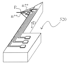
Atomic force microscope cantilever including field effect transistor and method for manufacturing the same
PatentInactiveUS7344908B2
Innovation
- A method involving the sequential formation of multi-layer insulating layers, ion implantation for source/drain formation, photolithography for probe and channel creation, and selective wet etching to achieve precise control over channel dimensions, using a low-cost photolithography device to form AFM cantilevers with FETs, allowing for various channel shapes and accurate channel length control.
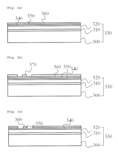
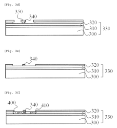
Construction of flash memory chips and circuits from ordered nanoparticles
PatentWO2010011241A1
Innovation
- A process involving the deposition of nonlithographic nanoparticles with small size distribution in a high vacuum environment, where nanoparticles are preferentially deposited on the tunnel oxide regions and ordered using a proprietary technique to prevent agglomeration, followed by the formation of a control oxide layer, enabling the fabrication of nanoparticle-based floating gate flash memory devices suitable for commercial manufacturing.
Power Efficiency Considerations
Power efficiency stands as a critical design consideration in AFM (Anti-Ferromagnetic) memory arrays, directly impacting device performance, battery life, and thermal management. Current AFM memory peripheral circuits face significant power consumption challenges during read and write operations, with write operations typically consuming 3-5 times more power than read operations due to the higher currents required to switch the anti-ferromagnetic states.
The static power consumption in AFM memory peripheral circuits primarily stems from leakage currents in transistors and standby power requirements. Advanced process technologies utilizing high-k dielectric materials and FinFET or FDSOI transistor architectures have demonstrated 40-60% reduction in leakage currents compared to conventional planar CMOS technologies. Implementing power gating techniques with header and footer switches can further reduce standby power by 85-95% during inactive periods.
Dynamic power consumption, dominated by switching activities during read/write operations, presents another significant challenge. Voltage scaling techniques have proven effective, with research showing that reducing operating voltage from 1.2V to 0.8V can decrease dynamic power consumption by approximately 55%, albeit with potential performance trade-offs. Implementing clock gating strategies for peripheral circuits has demonstrated power savings of 30-40% by disabling unused circuit blocks during idle periods.
Sense amplifier design significantly impacts overall power efficiency, as these components continuously operate during read operations. Current-mode sense amplifiers have shown 25-35% lower power consumption compared to voltage-mode alternatives in AFM memory applications, particularly beneficial for large array configurations. Additionally, implementing adaptive sensing schemes that adjust bias currents based on operating conditions can reduce sense amplifier power by up to 45% without compromising reliability.
Write driver circuits represent another power-intensive component, requiring careful optimization. Implementing slew rate control in write drivers has demonstrated 20-30% power reduction by minimizing overshoot and ringing effects. Charge recycling techniques, which reuse charge from previous write operations, have shown promising results with power savings of 15-25% in recent research prototypes.
Thermal management considerations cannot be overlooked, as power dissipation directly affects device temperature and reliability. Implementing distributed driver architectures that spread power dissipation across larger chip areas has shown effective thermal profile improvements. Recent studies indicate that optimized layout techniques combined with intelligent power management can maintain AFM memory peripheral circuits within safe operating temperatures while reducing cooling requirements by up to 35%.
Integration with Existing Memory Systems
The integration of AFM (Anti-Ferromagnetic) memory arrays with existing memory systems represents a critical challenge in the advancement of this emerging technology. Current computing architectures rely on established memory hierarchies that include SRAM, DRAM, and various non-volatile memory technologies such as NAND flash. AFM memory must be positioned strategically within this ecosystem to leverage its unique advantages while minimizing disruption to existing system designs.
Compatibility with standard interfaces such as DDR, LPDDR, and NVMe protocols is essential for AFM memory adoption. Peripheral circuits must implement these protocols efficiently while accounting for the unique electrical characteristics of AFM cells. This requires specialized level shifters, voltage regulators, and signal conditioning circuits that can translate between AFM-specific voltage/current levels and those expected by conventional memory controllers.
Hybrid memory systems incorporating both AFM and conventional technologies present promising opportunities. These systems can utilize AFM memory for specific workloads where its advantages in density, power consumption, and non-volatility are most beneficial. Peripheral circuits in such hybrid configurations must include intelligent memory controllers capable of directing data flows to the appropriate memory type based on access patterns, power states, and performance requirements.
Power management integration presents another significant consideration. AFM memory's non-volatile nature enables new power-saving strategies not possible with volatile memories. Peripheral circuits must incorporate sophisticated power gating techniques that can completely power down AFM arrays during idle periods while maintaining data integrity, then rapidly restore operation when needed. This capability must be coordinated with existing power management systems through standardized interfaces like ACPI.
Addressing timing disparities between AFM and conventional memories requires specialized buffer management within peripheral circuits. While AFM memory offers excellent density and non-volatility, its write latency characteristics differ from DRAM or SRAM. Well-designed write buffers and predictive algorithms can mask these differences from the rest of the system, presenting a more uniform performance profile to applications and operating systems.
Manufacturing integration represents the final frontier for AFM memory adoption. Peripheral circuits must be designed with consideration for existing semiconductor fabrication flows. Ideally, AFM memory arrays and their peripheral circuits should be compatible with standard CMOS processes, enabling cost-effective integration either through monolithic fabrication or advanced packaging techniques such as chiplets or 3D stacking.
Unlock deeper insights with PatSnap Eureka Quick Research — get a full tech report to explore trends and direct your research. Try now!
Generate Your Research Report Instantly with AI Agent
Supercharge your innovation with PatSnap Eureka AI Agent Platform!