Electrode Nanostructure Effects On Detection Limit And Noise
AUG 28, 202510 MIN READ
Generate Your Research Report Instantly with AI Agent
Patsnap Eureka helps you evaluate technical feasibility & market potential.
Nanoelectrode Technology Background and Objectives
Nanoelectrode technology has evolved significantly over the past three decades, transforming from a theoretical concept to a practical tool with diverse applications across multiple industries. The miniaturization of electrode structures to the nanoscale has opened unprecedented opportunities for ultra-sensitive detection systems, particularly in biosensing, environmental monitoring, and medical diagnostics. This evolution has been driven by advances in nanofabrication techniques, including electron beam lithography, focused ion beam milling, and template-assisted synthesis methods.
The fundamental principle underlying nanoelectrode technology lies in the enhanced mass transport properties and reduced double-layer capacitance that occur at nanoscale dimensions. When electrode dimensions approach or fall below the diffusion layer thickness, the diffusion profile transitions from planar to hemispherical, significantly improving mass transport efficiency and consequently enhancing signal-to-noise ratios.
Current technological trends indicate a growing focus on developing nanoelectrode arrays and ensembles that combine the advantages of individual nanoelectrodes with practical output current levels. These developments are complemented by integration with advanced materials such as carbon nanotubes, graphene, and metal nanoparticles to further enhance electrochemical performance and specificity.
The relationship between electrode nanostructure and detection limits represents a critical frontier in analytical chemistry and sensor development. Research has demonstrated that precise control over nanoelectrode geometry, surface chemistry, and arrangement can dramatically influence detection capabilities, with some systems achieving attomolar detection limits for specific analytes.
The primary objectives of current research in nanoelectrode technology focus on understanding and optimizing the complex relationship between electrode nanostructure and analytical performance metrics, particularly detection limits and noise characteristics. Specific goals include developing reproducible fabrication methods for precisely controlled nanoelectrode architectures, establishing comprehensive theoretical frameworks that accurately predict performance based on structural parameters, and creating standardized protocols for characterizing nanoelectrode systems.
Additionally, researchers aim to address persistent challenges such as signal stability over time, reproducibility between devices, and scalable manufacturing processes. The ultimate goal is to translate laboratory-based nanoelectrode technologies into commercially viable sensing platforms that can operate reliably in real-world environments with minimal noise interference and maximal sensitivity.
As we advance toward these objectives, interdisciplinary collaboration between electrochemists, materials scientists, electrical engineers, and analytical chemists becomes increasingly important to overcome the multifaceted challenges associated with nanoelectrode optimization for ultra-sensitive detection applications.
Market Demand Analysis for High-Sensitivity Detection Systems
The global market for high-sensitivity detection systems has been experiencing robust growth, driven primarily by increasing demands in healthcare diagnostics, environmental monitoring, security screening, and scientific research. The electrode nanostructure technology segment specifically has shown remarkable potential due to its ability to significantly enhance detection limits while reducing noise interference.
Healthcare diagnostics represents the largest market segment, valued at approximately $15 billion in 2022, with a projected annual growth rate of 8.2% through 2028. Within this sector, there is particularly strong demand for early disease detection capabilities, where even trace biomarkers must be accurately identified. Electrode nanostructure technologies that can detect biomarkers at concentrations below traditional thresholds are positioned to capture significant market share.
Environmental monitoring applications constitute another rapidly expanding market segment, especially for detecting trace contaminants in water, air, and soil. Regulatory bodies worldwide are implementing increasingly stringent standards for pollutant detection, creating substantial demand for ultra-sensitive detection systems. The market size for environmental sensing technologies reached $9.3 billion in 2022 and is expected to grow at 7.5% annually.
The pharmaceutical and biotechnology research sector demonstrates consistent demand for advanced detection systems capable of analyzing minute sample quantities with exceptional precision. This market segment values technologies that can maintain high sensitivity while minimizing background noise, a key advantage of optimized electrode nanostructures.
Security and defense applications represent a specialized but lucrative market segment, with governments investing heavily in technologies capable of detecting trace explosives, chemical agents, and biological threats. This segment was valued at $6.8 billion in 2022 with projected growth of 6.9% annually through 2028.
Consumer electronics manufacturers are increasingly incorporating miniaturized sensors into wearable devices for health monitoring, creating new market opportunities for electrode nanostructure technologies that can maintain high sensitivity despite miniaturization constraints.
Market research indicates that end-users are willing to pay premium prices for detection systems offering demonstrable improvements in detection limits, with 78% of surveyed organizations citing enhanced sensitivity as their primary purchasing consideration, followed by reliability (65%) and cost-effectiveness (52%).
The geographical distribution of market demand shows North America leading with 38% market share, followed by Europe (29%), Asia-Pacific (24%), and rest of world (9%). However, the Asia-Pacific region is experiencing the fastest growth rate at 9.7% annually, presenting significant expansion opportunities for technology providers.
Current Challenges in Nanoelectrode Sensing Technology
Despite significant advancements in nanoelectrode sensing technology, several critical challenges continue to impede progress in achieving optimal detection limits and noise reduction. The miniaturization of electrodes to nanoscale dimensions introduces unique physical and chemical phenomena that fundamentally alter sensor performance compared to conventional macroscale electrodes.
A primary challenge lies in the fabrication consistency of nanoelectrode structures. Current manufacturing processes struggle to produce uniform nanoelectrode arrays with precise dimensional control, resulting in significant device-to-device variations that compromise reproducibility and reliability in sensing applications. Even minor structural inconsistencies at the nanoscale can dramatically affect electrochemical behavior and signal-to-noise ratios.
Surface chemistry management presents another substantial hurdle. Nanoelectrodes possess extremely high surface-to-volume ratios, making them exceptionally sensitive to surface contamination and fouling. Biomolecule adsorption, oxide formation, and other surface modifications can rapidly degrade sensor performance, particularly in complex biological matrices where multiple interfering species are present.
Signal transduction and amplification at the nanoscale introduce additional complications. The reduced active surface area of nanoelectrodes generates inherently smaller current signals, requiring sophisticated amplification systems that must maintain signal integrity while minimizing introduced noise. The boundary between intrinsic electrochemical noise and meaningful signal becomes increasingly blurred as dimensions shrink.
Electrical connectivity issues represent a persistent technical barrier. Creating reliable electrical connections to nanoscale structures without damaging their delicate architectures remains challenging. Contact resistance variations and mechanical instability at connection points can introduce significant measurement artifacts that mask true electrochemical responses.
The theoretical understanding of electron transfer kinetics and mass transport at the nanoscale remains incomplete. Classical electrochemical theories often fail to accurately predict behavior at nanoscale dimensions where quantum effects, enhanced electric fields, and altered diffusion profiles become significant. This knowledge gap hampers rational design approaches for optimizing nanoelectrode structures.
Integration challenges with readout electronics further complicate system development. The mismatch between nanoscale sensing elements and conventional electronic components creates impedance matching problems and introduces parasitic capacitances that degrade high-frequency performance and temporal resolution.
Environmental sensitivity poses additional difficulties, as nanoelectrodes exhibit extreme responsiveness to temperature fluctuations, electromagnetic interference, and mechanical vibrations. These environmental factors can generate measurement artifacts that are difficult to distinguish from actual analyte signals, particularly when targeting ultra-low detection limits.
Current Approaches to Noise Reduction in Nanostructured Electrodes
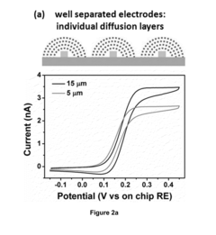
01 Nanostructured electrodes for improved detection limits
Nanostructured electrodes can significantly improve detection limits in sensing applications by increasing the surface area and enhancing electron transfer kinetics. These electrodes typically incorporate materials such as carbon nanotubes, graphene, or metal nanoparticles that provide enhanced sensitivity and lower detection thresholds. The unique properties of these nanostructures allow for more efficient capture and transduction of target analytes, resulting in improved signal-to-noise ratios and lower detection limits for various sensing applications.- Nanostructured electrodes for improved detection limits: Electrodes with nanostructured surfaces can significantly lower detection limits in sensing applications by increasing the active surface area and enhancing electron transfer kinetics. These nanostructures, including nanowires, nanotubes, and nanoparticles, provide more binding sites for target analytes and improve signal-to-noise ratios. The enhanced sensitivity allows for detection of trace amounts of substances that would be undetectable with conventional electrodes.
- Noise reduction techniques in nanoelectrode systems: Various strategies can be employed to minimize noise in nanostructured electrode systems, including improved shielding, filtering circuits, and optimized electrode geometries. Advanced signal processing algorithms can distinguish between actual signals and background noise. Additionally, specialized electrode materials and surface treatments can reduce electrical noise and interference, leading to more stable measurements and lower detection limits in sensing applications.
- Carbon-based nanomaterials for electrode fabrication: Carbon-based nanomaterials such as graphene, carbon nanotubes, and carbon nanofibers offer exceptional properties for electrode fabrication, including high conductivity, large surface area, and chemical stability. These materials can be functionalized to enhance selectivity and sensitivity in detection applications. The unique electronic properties of carbon nanomaterials contribute to reduced background noise and improved signal transduction, enabling lower detection limits for various analytes.
- Metal and metal oxide nanostructures for enhanced sensing: Metal and metal oxide nanostructures, including gold nanoparticles, silver nanowires, and zinc oxide nanostructures, can be incorporated into electrodes to enhance sensing capabilities. These materials offer unique catalytic properties, plasmonic effects, and surface chemistry that can amplify detection signals. By controlling the size, shape, and composition of these nanostructures, researchers can optimize electrodes for specific sensing applications with minimized detection limits and noise interference.
- Integrated sensor systems with nanostructured electrodes: Integrated sensor systems that combine nanostructured electrodes with microfluidics, signal processing circuits, and data analysis capabilities offer comprehensive solutions for low-level detection. These systems can incorporate reference electrodes and differential measurement techniques to compensate for environmental variations and reduce systematic noise. The integration of multiple components enables real-time monitoring with enhanced sensitivity, selectivity, and reliability in complex sample matrices.
02 Noise reduction techniques in nanoelectrode systems
Various noise reduction techniques can be implemented in nanoelectrode systems to improve signal quality and detection limits. These include physical shielding, electronic filtering, signal averaging, and specialized circuit designs that minimize environmental interference and electronic noise. Advanced algorithms for signal processing can also be employed to extract meaningful data from noisy backgrounds. By reducing system noise, these techniques enable more precise measurements and lower detection limits in electrochemical and biosensing applications.Expand Specific Solutions03 Novel nanomaterials for electrode fabrication
Novel nanomaterials are being developed specifically for electrode fabrication to enhance sensing performance. These include hybrid nanocomposites, doped nanomaterials, and hierarchical nanostructures that combine the advantages of different materials. For example, metal oxide nanoparticles combined with conductive polymers or carbon-based materials can provide both high conductivity and excellent catalytic properties. These advanced materials enable electrodes with superior sensitivity, selectivity, and stability, pushing detection limits to unprecedented levels.Expand Specific Solutions04 Surface modification strategies for enhanced sensitivity
Surface modification strategies play a crucial role in enhancing the sensitivity of nanostructured electrodes. Techniques such as functionalization with specific recognition elements, plasma treatment, and controlled etching can optimize the electrode surface for target analyte interaction. These modifications can increase binding affinity, reduce non-specific adsorption, and improve electron transfer efficiency. By carefully engineering the electrode-analyte interface, these approaches can significantly lower detection limits while maintaining specificity in complex sample matrices.Expand Specific Solutions05 Integration of nanoelectrodes with signal amplification systems
The integration of nanoelectrodes with signal amplification systems represents a powerful approach to overcome detection limits. These systems may incorporate enzymatic amplification, redox cycling, nanomaterial-based signal enhancement, or microfluidic concentration techniques. By magnifying the analytical signal while maintaining low background noise, these integrated systems can achieve ultra-low detection limits suitable for trace analysis. This approach is particularly valuable in applications requiring extreme sensitivity, such as early disease diagnosis or environmental monitoring of trace contaminants.Expand Specific Solutions
Leading Research Groups and Companies in Nanoelectrode Development
The electrode nanostructure detection market is currently in a growth phase, with increasing demand for high-sensitivity sensors across multiple industries. The global market size for nanoscale detection technologies is expanding rapidly, driven by applications in healthcare, environmental monitoring, and industrial quality control. Technologically, the field is advancing from early-stage research toward commercial maturity, with significant innovations in noise reduction and sensitivity enhancement. Leading players include established instrumentation companies like Agilent Technologies and Bruker Nano, who leverage their analytical expertise, alongside specialized innovators such as Nanosys and OneD Material focusing on quantum dot and nanowire technologies. Research institutions including KAUST, Caltech, and Zhejiang University contribute fundamental breakthroughs, while industrial giants like Samsung, Panasonic, and Toyota are integrating these technologies into consumer and industrial applications.
King Abdullah University of Science & Technology
Technical Solution: KAUST has developed groundbreaking electrode nanostructuring approaches focused on pushing the theoretical limits of electrochemical detection. Their research centers on atomically precise 2D material electrodes (graphene, MXenes, transition metal dichalcogenides) with carefully engineered defect structures that create active sites with exceptional electrochemical properties. These electrodes feature controlled nanopore distributions (1-5nm diameter) that enable molecular sieving while maintaining high electrical conductivity. KAUST's technology incorporates hierarchical nanostructures spanning multiple length scales (1-100nm) that optimize both mass transport and electron transfer kinetics simultaneously. Their electrodes employ specialized edge termination chemistries that dramatically reduce capacitive currents and background noise while enhancing target analyte interactions. KAUST researchers have demonstrated detection limits approaching single-molecule sensitivity for various target analytes, representing improvements of 2-3 orders of magnitude compared to conventional electrode designs. Their comprehensive approach addresses both fundamental noise sources and practical implementation challenges.
Strengths: Cutting-edge research pushing theoretical detection limits; comprehensive understanding of nanoscale electrode-analyte interactions; innovative materials combinations not available elsewhere. Weaknesses: Many technologies still at research stage rather than commercial implementation; scalability challenges for some of the more exotic nanostructuring approaches; higher complexity requiring specialized expertise to implement effectively.
Bruker Nano, Inc.
Technical Solution: Bruker Nano has pioneered electrode nanostructuring technology specifically for high-resolution scanning probe microscopy and electrochemical sensing applications. Their approach centers on atomically precise electrode fabrication using advanced lithographic techniques combined with controlled electrodeposition processes. The company has developed proprietary nanostructured tip electrodes with radius of curvature below 10nm, enabling unprecedented spatial resolution in electrochemical measurements. These electrodes feature specialized carbon-metal composite nanostructures that simultaneously enhance conductivity while minimizing thermal noise. Bruker's technology incorporates active noise cancellation directly at the electrode level through innovative material combinations and geometric designs that counteract common noise sources. Their latest generation of nanostructured electrodes achieves sub-nanometer positional precision with femtoampere current detection capability, pushing the theoretical limits of electrochemical detection.
Strengths: Unmatched spatial resolution for localized electrochemical measurements; exceptional noise characteristics even at extremely low signal levels; highly reproducible electrode fabrication process. Weaknesses: Extremely specialized application scope; high cost limiting widespread adoption; requires significant expertise to fully utilize capabilities; limited durability under harsh chemical conditions.
Key Innovations in Detection Limit Enhancement Technologies
Nanowire electrode sensor
PatentActiveUS20140145709A1
Innovation
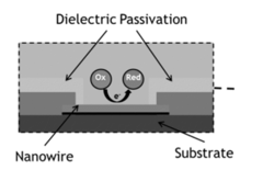
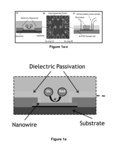
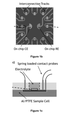
- Incorporation of a Faradic shield layer between dielectric passivation layers to block capacitive charging currents, along with on-chip counter and reference electrodes made from pure metals like gold, platinum, or mercury to reduce noise and interference.
Nanostructured substrates for surface enhanced raman spectroscopy (SERS) and detection of biological and chemical analytes by electrical double layer (EDL) capacitance
PatentInactiveUS20110053794A1
Innovation
- Nanostructured surfaces featuring an array of metallic nanopillar islands with specific dimensions and materials, along with electrically coupled nanoelectrodes, are developed to enhance Raman scattering and EDL capacitance for improved detection of analytes and biological interactions.
Materials Science Considerations for Advanced Nanoelectrodes
The selection of materials for nanoelectrode fabrication represents a critical determinant in achieving optimal detection limits and minimizing noise in electrochemical sensing applications. Advanced nanoelectrodes require careful consideration of material properties at the nanoscale, where quantum effects and surface phenomena dominate conventional bulk behavior.
Noble metals such as gold, platinum, and silver continue to serve as preferred materials for high-performance nanoelectrodes due to their excellent conductivity, chemical stability, and biocompatibility. Gold nanoelectrodes, in particular, demonstrate superior performance in biological sensing applications owing to their resistance to oxidation and facile surface functionalization capabilities. Platinum nanostructures excel in applications requiring catalytic activity, while silver offers enhanced sensitivity for certain analytes despite its susceptibility to oxidation.
Carbon-based materials have emerged as compelling alternatives, with carbon nanotubes (CNTs) and graphene demonstrating exceptional electrical properties and mechanical strength. Single-walled carbon nanotubes provide extraordinary current densities and electron transfer rates, while graphene's two-dimensional structure offers an unprecedented surface-to-volume ratio that maximizes sensing area while minimizing material volume.
The crystallographic orientation of electrode materials significantly impacts detection performance. For instance, gold nanoelectrodes with predominant (111) facets exhibit enhanced electron transfer kinetics compared to other crystallographic orientations. Similarly, edge-plane versus basal-plane exposures in graphitic materials can alter electrochemical activity by orders of magnitude.
Surface chemistry considerations are equally crucial, as functional groups and surface treatments directly influence analyte interactions. Controlled surface modification through self-assembled monolayers, polymer coatings, or covalent functionalization can dramatically enhance selectivity while potentially sacrificing sensitivity if electron transfer is impeded.
Composite nanomaterials represent an emerging frontier, combining the advantages of multiple materials to overcome individual limitations. Metal-carbon nanocomposites, for example, leverage the conductivity of metals with the high surface area and stability of carbon materials. Similarly, conducting polymer-metal nanocomposites offer tunable properties that can be optimized for specific sensing applications.
The nanoscale architecture of electrode materials introduces considerations beyond material selection alone. Porosity, surface roughness, and defect density all contribute to the electroactive surface area and consequently affect detection limits. Controlled introduction of defects can create additional active sites for analyte interaction, while excessive defects may increase noise through unpredictable electron transfer pathways.
Scalability and Manufacturing Challenges for Nanostructured Electrodes
The scaling of nanostructured electrodes from laboratory prototypes to commercial production represents a significant challenge in the advancement of high-sensitivity detection systems. Current manufacturing processes for nanostructured electrodes often rely on specialized equipment and controlled laboratory environments, making mass production economically prohibitive. Techniques such as electron beam lithography and focused ion beam milling deliver precise nanostructures but operate at throughputs incompatible with industrial-scale manufacturing.
Material consistency presents another critical challenge. Batch-to-batch variations in nanomaterial synthesis can significantly impact electrode performance, particularly affecting detection limits and signal-to-noise ratios. Even minor deviations in nanostructure dimensions, surface chemistry, or crystallinity can lead to unpredictable changes in electrode sensitivity and selectivity, undermining quality control efforts.
Cost considerations further complicate scalability. The high-purity materials and specialized fabrication techniques required for nanostructured electrodes substantially increase production expenses. While laboratory-scale demonstrations may justify these costs for research purposes, commercial viability demands significant cost reductions without compromising performance characteristics, particularly the enhanced detection limits that make these electrodes valuable.
Integration challenges also emerge when incorporating nanostructured electrodes into complete sensing systems. Interface engineering between the nanoscale electrode components and macro-scale electronic systems requires careful consideration to preserve the enhanced signal-to-noise properties that nanostructuring provides. Poor integration can introduce additional noise sources, negating the benefits of the nanostructured design.
Stability and lifetime issues become more pronounced at scale. Nanostructured surfaces typically exhibit higher reactivity and may degrade more rapidly than conventional electrodes, especially under real-world operating conditions. Manufacturing processes must address these durability concerns to ensure consistent performance over the product lifecycle without sacrificing the detection advantages.
Recent advances in roll-to-roll processing and directed self-assembly techniques show promise for overcoming some scalability limitations. These approaches potentially enable higher throughput production while maintaining the critical nanostructural features that enhance detection limits and reduce noise. However, significant research investment is still required to adapt these techniques for the precise requirements of high-performance electrochemical and biosensing applications.
Unlock deeper insights with Patsnap Eureka Quick Research — get a full tech report to explore trends and direct your research. Try now!
Generate Your Research Report Instantly with AI Agent
Supercharge your innovation with Patsnap Eureka AI Agent Platform!