

Mass Production Challenges For Nanostructured Electrodes
AUG 28, 20259 MIN READ
Generate Your Research Report Instantly with AI Agent
Patsnap Eureka helps you evaluate technical feasibility & market potential.
Nanostructured Electrode Technology Evolution and Objectives
Nanostructured electrodes have emerged as a transformative technology in energy storage and conversion systems over the past two decades. The evolution of this technology began in the early 2000s with rudimentary attempts to increase electrode surface area through simple nanoparticle formulations. By 2010, researchers had developed more sophisticated approaches including nanowires, nanotubes, and hierarchical structures that dramatically enhanced electrochemical performance in laboratory settings.
The technological trajectory has been driven by the fundamental limitations of conventional electrode materials, particularly in lithium-ion batteries, supercapacitors, and fuel cells. Traditional electrodes suffer from limited active surface area, poor ion transport kinetics, and structural degradation during cycling. Nanostructuring addresses these challenges by providing shorter diffusion paths for ions, increased electrode-electrolyte contact area, and improved mechanical stability during charge-discharge cycles.
Recent advancements have focused on three-dimensional nanoarchitectures, including aerogels, nanofoams, and ordered mesoporous structures. These designs optimize both electronic and ionic conductivity while maintaining structural integrity under operational conditions. Particularly noteworthy is the development of hybrid nanostructures that combine different materials at the nanoscale to create synergistic effects that enhance overall performance.
The primary objective of nanostructured electrode research is to bridge the gap between laboratory demonstrations and industrial implementation. This includes developing scalable synthesis methods that maintain precise control over nanoscale features while being compatible with existing manufacturing infrastructure. Additionally, researchers aim to enhance the long-term stability of nanostructured electrodes, as surface reactivity often increases with decreasing particle size, potentially leading to accelerated degradation.
Another critical goal is reducing production costs to competitive levels. Current laboratory-scale synthesis methods often involve expensive precursors, complex equipment, or energy-intensive processes that are prohibitive for mass production. The field is therefore evolving toward greener synthesis routes and earth-abundant materials that maintain performance while improving economic viability.
Looking forward, the technology roadmap emphasizes developing standardized characterization protocols to accurately assess nanostructured electrodes across different applications and manufacturing processes. This standardization will facilitate technology transfer from research institutions to industry partners and accelerate commercialization timelines. The ultimate objective remains creating nanostructured electrodes that deliver superior performance while meeting the stringent cost, durability, and safety requirements of commercial energy storage and conversion systems.
Market Analysis for Nanostructured Electrode Applications
The global market for nanostructured electrode applications is experiencing robust growth, driven by increasing demand across multiple sectors including energy storage, electronics, healthcare, and environmental applications. The market value for nanostructured electrodes reached approximately $3.2 billion in 2022 and is projected to grow at a compound annual growth rate (CAGR) of 14.7% through 2028, potentially reaching $7.1 billion by the end of the forecast period.
Energy storage represents the largest application segment, accounting for nearly 45% of the total market share. Within this segment, lithium-ion batteries dominate due to their widespread use in electric vehicles, portable electronics, and grid storage systems. The electric vehicle market alone is expected to consume over 30% of all nanostructured electrodes produced globally by 2025, reflecting the automotive industry's accelerating shift toward electrification.
Consumer electronics constitutes the second-largest market segment at approximately 25% market share, with applications in smartphones, wearables, and other portable devices. The miniaturization trend in electronics continues to drive demand for higher energy density and faster charging capabilities that nanostructured electrodes can provide.
Healthcare applications, including biosensors, drug delivery systems, and diagnostic tools, represent a rapidly growing segment with an estimated 18% CAGR through 2028. The superior sensitivity and specificity of nanostructured electrodes make them particularly valuable for point-of-care diagnostics and personalized medicine applications.
Regionally, Asia-Pacific dominates the market with approximately 45% share, led by China, Japan, and South Korea. This dominance stems from the region's strong manufacturing base for electronics and batteries, coupled with significant government investments in nanotechnology research. North America and Europe follow with approximately 28% and 22% market shares respectively, with particular strength in healthcare and specialized industrial applications.
Market penetration faces several barriers including high production costs, scalability challenges, and regulatory uncertainties. The average cost of nanostructured electrodes remains 2.5-4 times higher than conventional alternatives, limiting adoption in price-sensitive applications. However, this gap is narrowing as production technologies mature and economies of scale improve.
Customer requirements are evolving toward higher performance specifications, with particular emphasis on cycle life, power density, and environmental sustainability. End-users increasingly demand electrodes that can deliver at least 1,000 charge-discharge cycles while maintaining 80% capacity, a benchmark that is driving continuous innovation in nanomaterial design and manufacturing processes.
Current Manufacturing Limitations and Technical Barriers
Despite significant advancements in nanostructured electrode technology, scaling production from laboratory to industrial levels remains a formidable challenge. Current manufacturing processes face substantial limitations in maintaining consistent quality across large-scale production. Conventional electrode fabrication techniques like screen printing and slot-die coating struggle to preserve the precise nanoscale features that give these electrodes their superior performance characteristics. When scaled up, these methods often result in structural defects, non-uniform particle distribution, and compromised electrochemical properties.
Material handling presents another significant barrier, as nanomaterials exhibit strong tendency to agglomerate during processing due to their high surface energy. This agglomeration disrupts the intended nanostructure and diminishes the electrochemical performance advantages. Additionally, the specialized equipment required for nanomaterial processing often lacks standardization across different manufacturing scales, creating inconsistencies when transitioning from pilot to full-scale production.
Cost-effectiveness remains a critical obstacle, with current manufacturing approaches requiring expensive precursors, specialized equipment, and energy-intensive processing conditions. Many promising laboratory techniques employ costly vacuum systems, high-temperature treatments, or complex multi-step processes that become economically prohibitive at industrial scales. The capital investment required for dedicated nanomanufacturing facilities often outweighs the performance benefits for many commercial applications.
Quality control and characterization present unique challenges at the nanoscale. Existing in-line monitoring techniques lack the resolution and throughput needed to effectively assess nanoscale features during high-volume production. This limitation creates significant quality assurance gaps, as defects may go undetected until final testing, resulting in high rejection rates and material waste.
Environmental and safety concerns further complicate manufacturing scale-up. Nanomaterials often require specialized handling protocols to mitigate potential health risks, while waste streams containing nanomaterials demand specialized treatment. Current regulatory frameworks remain underdeveloped for nanomanufacturing processes, creating uncertainty for industrial implementation.
Process integration represents perhaps the most significant technical barrier, as nanostructured electrodes must ultimately be incorporated into complete energy storage devices. The interfaces between nanoscale components and conventional device architectures often create compatibility issues during assembly. Existing manufacturing lines designed for traditional electrodes require substantial modification to accommodate the unique requirements of nanostructured alternatives, creating significant barriers to adoption by established manufacturers.
Current Mass Production Methodologies
01 Fabrication methods for nanostructured electrodes
Various fabrication methods can be employed to mass produce nanostructured electrodes, including chemical vapor deposition, electrodeposition, and template-assisted synthesis. These methods allow for precise control over the nanostructure morphology, size, and composition, which are critical for electrode performance. Advanced techniques enable the creation of high-surface-area electrodes with enhanced electrochemical properties suitable for large-scale production.- Nanofabrication techniques for electrode mass production: Various nanofabrication techniques are employed for the mass production of nanostructured electrodes, including lithography, template-assisted synthesis, and vapor deposition methods. These techniques allow for precise control over the size, shape, and arrangement of nanostructures, which is crucial for optimizing electrode performance. Advanced manufacturing processes enable the scalable production of nanostructured electrodes with consistent quality and properties for commercial applications.
- Roll-to-roll processing for continuous electrode fabrication: Roll-to-roll (R2R) processing enables continuous, high-throughput fabrication of nanostructured electrodes on flexible substrates. This manufacturing approach involves sequential deposition, patterning, and treatment steps on a moving substrate, allowing for efficient mass production. The technique is particularly valuable for producing large-area electrodes for energy storage devices, solar cells, and flexible electronics, offering significant cost advantages over batch processing methods.
- Solution-based synthesis methods for nanostructured materials: Solution-based synthesis methods, including sol-gel processing, hydrothermal/solvothermal synthesis, and chemical reduction approaches, offer scalable routes for producing nanostructured electrode materials. These methods enable precise control over composition, morphology, and crystal structure while being amenable to large-scale production. The resulting nanomaterials can be formulated into inks or pastes for subsequent electrode fabrication through printing or coating techniques.
- Additive manufacturing and 3D printing of electrodes: Additive manufacturing and 3D printing technologies enable the fabrication of complex, three-dimensional nanostructured electrodes with customizable architectures. These approaches allow for precise control over porosity, surface area, and internal structure, which are critical for optimizing electrochemical performance. The layer-by-layer deposition process can incorporate nanomaterials into printable inks, enabling scalable production of electrodes with enhanced surface area and improved mass transport properties.
- Quality control and characterization methods for mass-produced electrodes: Effective quality control and characterization methods are essential for ensuring consistency in mass-produced nanostructured electrodes. Advanced analytical techniques, including electron microscopy, spectroscopy, and electrochemical testing, are employed to monitor structural features, composition, and performance metrics throughout the manufacturing process. In-line monitoring systems and automated inspection tools enable real-time quality assessment, reducing defects and ensuring uniform electrode properties in large-scale production.
02 Roll-to-roll manufacturing processes
Roll-to-roll manufacturing processes represent a scalable approach for continuous production of nanostructured electrodes. This technique allows for high-throughput fabrication on flexible substrates, enabling cost-effective mass production. The process typically involves deposition of nanomaterials onto moving substrates, followed by subsequent processing steps such as drying, sintering, or patterning, all performed in a continuous manner.Expand Specific Solutions03 Carbon-based nanostructured electrode materials
Carbon-based materials, including carbon nanotubes, graphene, and carbon nanofibers, are widely used in nanostructured electrodes due to their excellent electrical conductivity, high surface area, and mechanical stability. Mass production techniques for these materials include chemical vapor deposition, arc discharge, and laser ablation methods. These materials can be functionalized or combined with other nanomaterials to enhance their electrochemical performance for various applications.Expand Specific Solutions04 Metal oxide nanostructures for electrode applications
Metal oxide nanostructures, such as titanium dioxide, zinc oxide, and iron oxide, are important materials for nanostructured electrodes. Mass production methods include sol-gel processes, hydrothermal synthesis, and electrochemical deposition. These materials offer advantages such as high stability, tunable electronic properties, and diverse morphologies including nanowires, nanoparticles, and nanosheets, making them suitable for various electrochemical applications.Expand Specific Solutions05 Quality control and characterization techniques
Effective quality control and characterization techniques are essential for the mass production of nanostructured electrodes. These include electron microscopy, X-ray diffraction, electrochemical impedance spectroscopy, and in-line monitoring systems. Advanced characterization methods ensure consistency in nanomaterial properties, electrode performance, and manufacturing reproducibility, which are critical factors for commercial-scale production and application of nanostructured electrodes.Expand Specific Solutions
Industry Leaders and Competitive Landscape
The mass production of nanostructured electrodes faces significant challenges in a rapidly evolving market currently transitioning from research to early commercialization. The global market for these advanced materials is projected to grow substantially, driven by applications in energy storage, electronics, and medical devices. From a technological maturity perspective, academic institutions like Northwestern University and University of Washington are leading fundamental research, while companies such as SMOLTEK AB and Sony Group Corp. are advancing manufacturing scalability. Chinese institutions including Dalian Institute of Chemical Physics and Shandong University are making significant progress in cost-effective production methods. The industry is characterized by a competitive landscape where collaboration between research institutions and industrial players is essential to overcome the technical barriers of consistent quality, scalability, and cost-effectiveness in mass production.
SMOLTEK AB
Technical Solution: SMOLTEK has developed a specialized carbon nanofiber (CNF) electrode manufacturing technology based on catalytic chemical vapor deposition (CCVD). Their process enables direct growth of vertically aligned carbon nanostructures on various substrate materials at temperatures compatible with standard manufacturing processes (below 390°C). The company's proprietary catalyst system allows precise control over nanofiber density (up to 10^10 fibers/cm²), diameter (50-200 nm), and height (0.1-10 μm). SMOLTEK's manufacturing approach eliminates the need for binders and additional conductive additives, creating electrodes with exceptional electrical conductivity and electrochemical performance. Their process has been demonstrated on wafer-scale production and is being scaled to roll-to-roll manufacturing for energy storage applications.
Strengths: SMOLTEK's direct growth approach eliminates several processing steps required in conventional electrode manufacturing, potentially reducing production costs and improving quality. Their technology creates nanostructured electrodes with exceptional electrical properties and structural stability. Weaknesses: The CVD process requires specialized equipment and precise control of process gases, which may present challenges for very large-scale production and safety management.
Honeywell International Technologies Ltd.
Technical Solution: Honeywell has developed an advanced manufacturing platform for nanostructured electrodes that combines sol-gel processing with precision coating technologies. Their approach creates hierarchical nanostructures with controlled macro, micro, and nanoscale features that optimize both ion transport and electron conduction. The company's manufacturing system incorporates real-time process monitoring using advanced sensors that track nanostructure formation during production, enabling closed-loop control of critical parameters. Honeywell has implemented specialized drying and curing processes that prevent nanostructure collapse during solvent removal, a common challenge in mass production. Their technology platform can produce nanostructured electrodes at thicknesses ranging from 10-200 μm with precise control over porosity gradients throughout the electrode structure.
Strengths: Honeywell's extensive experience in process automation and quality control systems provides exceptional consistency in nanostructured electrode production. Their technology offers excellent thickness control and structural uniformity. Weaknesses: The sol-gel approach requires careful handling of potentially hazardous precursors, and the multi-step process can introduce complexity in manufacturing logistics and quality assurance.
Key Patents and Breakthroughs in Nanofabrication
Method for producing nanostructured layers
PatentWO2016198033A1
Innovation
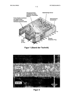
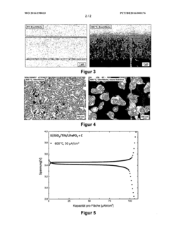
- A method using magnetron sputtering with a ceramic target and controlled process parameters to produce nanostructured electrodes in a single step, achieving a fibrous, porous network structure without the need for binders or toxic solvents, by depositing active material directly onto a substrate at elevated temperatures.
Nanostructured electrodes and active polymer layers
PatentWO2012021739A1
Innovation
- A method involving a reusable mold with nano-concavities to create nanoarchitectured polymer layers, which are then transferred to a substrate and coated with electrode materials, allowing for the production of nanostructured electrodes with tunable dimensions and distribution, enabling high-throughput manufacturing without the need for sacrificial templates.

Supply Chain Considerations for Raw Materials
The secure and sustainable supply of raw materials represents a critical bottleneck in scaling nanostructured electrode production from laboratory to industrial levels. Current manufacturing processes rely heavily on rare earth elements, precious metals, and specialized nanomaterials that face significant supply constraints and price volatility. For instance, materials such as lithium, cobalt, and platinum group metals experience frequent market fluctuations due to geopolitical tensions, limited mining locations, and increasing global demand across multiple industries.
Material purity requirements present another substantial challenge, as nanostructured electrodes typically demand exceptionally high-grade precursors with minimal contaminants. Even trace impurities can dramatically impact electrochemical performance, necessitating sophisticated purification processes that add complexity and cost to the supply chain. This creates a delicate balance between material quality and economic viability that manufacturers must carefully navigate.
Geographic concentration of critical raw materials further complicates supply chain resilience. Over 70% of cobalt production occurs in the Democratic Republic of Congo, while China controls approximately 85% of rare earth processing capacity globally. This concentration creates vulnerability to trade restrictions, export quotas, and regional conflicts that can severely disrupt production schedules and increase costs unpredictably.
Emerging alternatives to traditional materials show promise but remain underdeveloped from a supply chain perspective. Silicon-based anodes, sodium-ion technologies, and carbon-derived nanomaterials offer potential pathways to reduce dependency on critical materials, yet their own supply chains lack the maturity and scale of established materials. Manufacturers pursuing these alternatives must consider not only technical performance but also the development timeline for reliable material sourcing networks.
Recycling and circular economy approaches are increasingly viewed as essential components of sustainable nanostructured electrode production. Current recycling rates for battery materials remain below 5% globally, representing both a challenge and opportunity. Advanced recycling technologies capable of recovering nanomaterials with minimal degradation could significantly reduce supply pressures, though these processes require further development to achieve economic viability at industrial scale.
Vertical integration strategies are being adopted by leading manufacturers to mitigate supply chain risks. Companies like Tesla and CATL have invested directly in mining operations and material processing facilities to secure priority access to critical materials. This approach requires substantial capital investment but provides greater control over material specifications, quality, and availability—critical factors for consistent mass production of nanostructured electrodes.
Sustainability and Environmental Impact Assessment
The environmental impact of nanostructured electrode mass production represents a critical consideration in the sustainable development of advanced energy storage technologies. Current manufacturing processes for these electrodes often involve energy-intensive methods, hazardous chemicals, and rare materials that pose significant sustainability challenges. The carbon footprint associated with high-temperature synthesis processes and vacuum-based deposition techniques is particularly concerning, with some estimates suggesting energy consumption rates of 50-100 kWh per kilogram of produced electrode material.
Waste generation during nanomaterial synthesis presents another substantial environmental concern. Chemical vapor deposition and wet chemical processes typically generate hazardous byproducts requiring specialized disposal protocols. Studies indicate that for every kilogram of nanostructured electrode material produced, approximately 10-15 kilograms of waste may be generated, including toxic solvents, unreacted precursors, and contaminated water.
Resource depletion represents a long-term sustainability challenge, particularly regarding rare earth elements and precious metals commonly used in high-performance electrodes. The mining and processing of these materials cause significant ecological disruption, including habitat destruction, water pollution, and soil contamination. Life cycle assessments reveal that the environmental burden of resource extraction often exceeds that of the manufacturing process itself.
Water usage in nanomaterial production processes presents another environmental pressure point. Purification steps and wet chemical methods can consume 200-500 liters of water per kilogram of electrode material. In regions facing water scarcity, this intensive consumption pattern raises serious sustainability questions about large-scale manufacturing feasibility.
Emerging regulatory frameworks worldwide are increasingly addressing these environmental concerns. The European Union's REACH regulations and similar initiatives in North America and Asia are establishing stricter guidelines for nanomaterial production, handling, and disposal. These regulations are driving innovation toward greener synthesis routes and more sustainable manufacturing approaches.
Promising developments in green chemistry approaches offer potential pathways to mitigate these environmental impacts. Aqueous-based synthesis methods, room-temperature processes, and solvent recycling systems have demonstrated potential to reduce both energy consumption and waste generation by 30-60% compared to conventional methods. Additionally, biomass-derived precursors and templates are emerging as renewable alternatives to petroleum-based chemicals traditionally used in nanostructure synthesis.
Closed-loop manufacturing systems represent perhaps the most comprehensive approach to environmental sustainability in this field. By integrating material recovery, waste treatment, and energy recapture systems, these holistic production frameworks aim to minimize external environmental impacts while maximizing resource efficiency throughout the electrode lifecycle.
Unlock deeper insights with Patsnap Eureka Quick Research — get a full tech report to explore trends and direct your research. Try now!
Generate Your Research Report Instantly with AI Agent
Supercharge your innovation with Patsnap Eureka AI Agent Platform!