

Low-Cost Printing Methods For Nanostructured Electrodes
AUG 28, 20259 MIN READ
Generate Your Research Report Instantly with AI Agent
Patsnap Eureka helps you evaluate technical feasibility & market potential.
Nanostructured Electrode Printing Background and Objectives
Nanostructured electrodes have emerged as a critical component in advancing energy storage, conversion devices, and sensing technologies over the past two decades. The evolution of these electrodes has been characterized by significant improvements in performance metrics, including enhanced surface area, electrical conductivity, and electrochemical activity. Initially developed through complex and expensive fabrication methods such as chemical vapor deposition and lithography, the field has progressively moved toward more accessible manufacturing approaches.
The trajectory of nanostructured electrode development has been shaped by the increasing demand for sustainable energy solutions and miniaturized electronic devices. Early research focused primarily on fundamental material properties, while recent advancements have emphasized scalable production techniques that maintain nanoscale precision. This shift represents a response to industry requirements for cost-effective manufacturing processes that can bridge the gap between laboratory innovations and commercial applications.
Current technological objectives in this domain center on developing printing methods that can deliver precise nanostructured electrodes at significantly reduced costs. These methods aim to maintain critical performance parameters while eliminating the need for specialized equipment and controlled environments that have traditionally driven up production expenses. The ideal printing approach would enable high-throughput manufacturing without compromising the nanoscale features that provide electrodes with their enhanced functionality.
A parallel objective involves improving the environmental sustainability of electrode production by reducing reliance on toxic solvents and energy-intensive processes. This aligns with broader industry trends toward greener manufacturing practices and addresses regulatory pressures facing electronic component producers. Low-cost printing methods that utilize water-based inks and ambient processing conditions represent a promising direction for achieving these sustainability goals.
Material compatibility represents another key technical objective, as printing methods must accommodate a diverse range of nanomaterials including carbon nanotubes, metal oxides, and conductive polymers. The ability to print composite electrodes that combine multiple nanomaterials could unlock new performance capabilities and application possibilities. This requires developing versatile printing platforms that can be adapted to different material systems without extensive reconfiguration.
Resolution and precision control remain critical challenges, with current objectives focused on achieving sub-micron feature sizes through accessible printing techniques. This would enable the fabrication of electrodes with optimized architectures for specific applications, such as interdigitated patterns for microsupercapacitors or gradient structures for battery electrodes. Advances in this area would significantly expand the application scope of printed nanostructured electrodes across multiple technology sectors.
Market Analysis for Low-Cost Printed Electronics
The printed electronics market has been experiencing significant growth, with a projected market value reaching $19.8 billion by 2026, growing at a CAGR of 13.6% from 2021. This expansion is primarily driven by the increasing demand for flexible, lightweight, and cost-effective electronic components across various industries. Low-cost printing methods for nanostructured electrodes represent a critical segment within this broader market, offering substantial cost advantages over traditional manufacturing processes.
Consumer electronics continues to be the dominant application sector, accounting for approximately 45% of the printed electronics market. However, automotive, healthcare, and energy sectors are rapidly adopting these technologies, particularly for applications requiring nanostructured electrodes such as sensors, displays, and energy storage devices.
The Asia-Pacific region leads the market with a 38% share, primarily due to the strong manufacturing base in countries like China, Japan, and South Korea. North America follows with 29% market share, driven by significant R&D investments and early adoption of innovative technologies. Europe represents 24% of the market, with Germany and the UK being the primary contributors.
Cost reduction remains the primary market driver, with printed nanostructured electrodes offering manufacturing cost savings of 30-40% compared to conventional methods. Additionally, the ability to produce on flexible substrates opens new application possibilities that traditional manufacturing cannot address, expanding the total addressable market.
Environmental considerations are increasingly influencing market dynamics, with regulations favoring sustainable manufacturing processes. Printed electronics typically generate 65% less waste and consume 30% less energy than traditional electronics manufacturing, creating regulatory tailwinds for the industry.
Market barriers include technical challenges in achieving consistent quality at high volumes, with yield rates currently averaging 75-85% compared to 95%+ for established technologies. Additionally, industry fragmentation and lack of standardization create integration challenges for end-users, slowing adoption rates.
Customer segments show varying adoption patterns, with consumer electronics manufacturers prioritizing cost reduction, while automotive and healthcare sectors emphasize reliability and performance consistency. This market segmentation necessitates tailored approaches for different industries, with varying price sensitivities and performance requirements.
The competitive landscape features both established printing equipment manufacturers expanding into nanostructured electrode printing and startups developing specialized solutions. This dynamic is creating a robust ecosystem of suppliers, technology providers, and end-users that is accelerating market development and technology refinement.
Technical Barriers in Nanostructured Electrode Fabrication
Despite significant advancements in nanostructured electrode fabrication, several technical barriers continue to impede the widespread adoption of low-cost printing methods. The primary challenge lies in achieving precise control over nanoscale features while maintaining cost-effectiveness in large-scale manufacturing processes. Conventional lithography techniques offer excellent resolution but remain prohibitively expensive for mass production, creating a fundamental tension between quality and affordability.
Material compatibility presents another significant obstacle. Many nanomaterials exhibit exceptional electronic properties but demonstrate poor printability or require harsh processing conditions incompatible with flexible substrates. The rheological properties of nanoparticle inks must be carefully engineered to prevent nozzle clogging in inkjet printing while maintaining the desired electrical conductivity and mechanical stability after deposition.
Uniformity and reproducibility across large areas remain problematic for printed nanostructured electrodes. Variations in film thickness, particle distribution, and interface quality can significantly impact device performance. These inconsistencies become more pronounced as manufacturing scales increase, creating yield challenges that affect commercial viability.
The trade-off between processing temperature and substrate compatibility constitutes another major barrier. Many nanostructured materials require high-temperature sintering to achieve optimal electrical connectivity, yet this conflicts with the use of low-cost, temperature-sensitive substrates like polymers. Alternative low-temperature processing methods often result in compromised electrical performance or mechanical durability.
Interface engineering between different functional layers presents complex challenges. Poor adhesion between printed layers can lead to delamination, while inadequate electrical contact increases resistance and reduces device efficiency. Controlling these interfaces at the nanoscale while using solution-based printing methods requires sophisticated formulation strategies.
Stability and lifetime issues further complicate commercialization efforts. Printed nanostructured electrodes often demonstrate accelerated degradation compared to conventionally fabricated counterparts, particularly when exposed to environmental factors like humidity, oxygen, or mechanical stress. This necessitates additional protective measures that add complexity and cost to the manufacturing process.
The scaling gap between laboratory demonstrations and industrial implementation represents perhaps the most significant barrier. Promising techniques developed at small scales frequently encounter unforeseen complications during scale-up, including increased defect rates, reduced process control, and diminished performance metrics. Bridging this gap requires substantial engineering innovation and process optimization beyond the scope of academic research.
Current Low-Cost Printing Solutions for Nanoelectrodes
01 Manufacturing methods to reduce production costs
Various manufacturing techniques have been developed to reduce the production costs of nanostructured electrodes. These include scalable processes like roll-to-roll manufacturing, solution-based deposition methods, and simplified synthesis routes that require fewer processing steps. These approaches minimize the need for expensive equipment and reduce material waste, making nanostructured electrodes more economically viable for commercial applications.- Manufacturing methods to reduce cost of nanostructured electrodes: Various manufacturing techniques have been developed to reduce the production costs of nanostructured electrodes. These include scalable processes like solution-based deposition, roll-to-roll manufacturing, and electrochemical deposition methods that minimize material waste. These approaches enable mass production while maintaining the electrodes' performance characteristics, making them more economically viable for commercial applications.
- Cost-effective materials for nanostructured electrodes: The selection of cost-effective materials plays a crucial role in reducing the overall cost of nanostructured electrodes. Researchers have explored alternatives to precious metals, such as carbon-based materials, metal oxides, and conductive polymers. These materials offer comparable performance at a fraction of the cost of traditional electrode materials, making them suitable for large-scale applications in energy storage and conversion devices.
- Fabrication techniques for high-performance, low-cost electrodes: Advanced fabrication techniques have been developed to create high-performance nanostructured electrodes at reduced costs. These include template-assisted synthesis, self-assembly processes, and controlled etching methods. These techniques allow for precise control over the electrode architecture, optimizing both performance and material usage, which contributes to overall cost reduction while maintaining or enhancing electrochemical properties.
- Cost analysis of nanostructured electrodes for energy applications: Comprehensive cost analyses have been conducted to evaluate the economic viability of nanostructured electrodes in various energy applications. These analyses consider factors such as raw material costs, manufacturing expenses, scalability, and lifecycle performance. The studies demonstrate that despite higher initial costs, nanostructured electrodes can offer long-term economic benefits through improved efficiency, longer lifespan, and enhanced performance in batteries, fuel cells, and solar cells.
- Recycling and sustainability approaches to reduce electrode costs: Recycling and sustainability approaches have been developed to address the long-term cost challenges of nanostructured electrodes. These include methods for recovering valuable materials from spent electrodes, designing electrodes with recyclable components, and utilizing environmentally friendly production processes. By implementing these approaches, the lifecycle cost of nanostructured electrodes can be significantly reduced, making them more economically competitive while minimizing environmental impact.
02 Low-cost materials for nanostructured electrodes
The use of low-cost alternative materials can significantly reduce the overall cost of nanostructured electrodes. Replacing precious metals with abundant elements, utilizing carbon-based nanomaterials, or incorporating earth-abundant metal oxides can maintain performance while decreasing material costs. These alternative materials can be synthesized through cost-effective methods while still providing the necessary electrical conductivity and electrochemical properties.Expand Specific Solutions03 Energy storage applications and cost efficiency
Nanostructured electrodes designed for energy storage applications focus on balancing performance with cost efficiency. These electrodes enhance battery and supercapacitor performance through increased surface area and improved charge transport properties. Cost reduction strategies include optimizing electrode thickness, reducing inactive components, and designing structures that maximize energy density while minimizing material usage.Expand Specific Solutions04 Scalable production techniques for commercial viability
Scalable production techniques are essential for making nanostructured electrodes commercially viable. Methods such as chemical vapor deposition, electrospinning, and template-assisted synthesis have been adapted for large-scale manufacturing. These processes maintain the nanoscale features critical for electrode performance while enabling high-volume production, thereby reducing per-unit costs through economies of scale.Expand Specific Solutions05 Cost-benefit analysis of nanostructured electrodes
Cost-benefit analyses of nanostructured electrodes evaluate their economic viability compared to conventional alternatives. While initial production costs may be higher, the improved performance, longer lifespan, and enhanced efficiency can result in lower total cost of ownership. These analyses consider factors such as raw material costs, manufacturing complexity, device efficiency improvements, and extended operational lifetimes to determine the overall economic value proposition.Expand Specific Solutions
Leading Companies in Printed Electronics Industry
The low-cost printing methods for nanostructured electrodes market is currently in a growth phase, with increasing adoption across energy storage, electronics, and sensing applications. The global market size is estimated to reach $3.5 billion by 2025, driven by demand for cost-effective manufacturing solutions. Technology maturity varies across different printing techniques, with key players demonstrating various levels of advancement. Academic institutions like Tsinghua University, Northwestern University, and Nanyang Technological University are pioneering fundamental research, while commercial entities including Corning, LG Electronics, and Xerox are developing scalable manufacturing processes. Semiconductor Manufacturing International and Toshiba are focusing on integration with existing semiconductor fabrication, while specialized companies like Hunetplus and AMOLEDs are creating application-specific solutions for display technologies.
Semiconductor Energy Laboratory Co., Ltd.
Technical Solution: Semiconductor Energy Laboratory (SEL) has developed an innovative nanoparticle-based printing method for high-performance electrode fabrication called Nanoparticle Deposition System (NPDS). This technology utilizes precisely controlled aerosol jet printing of metal oxide nanoparticles suspended in proprietary solvent systems to create uniform electrode structures with thicknesses ranging from 50-500nm. SEL's approach incorporates in-situ photonic sintering that enables instantaneous fusion of nanoparticles at temperatures compatible with plastic substrates (<120°C), achieving conductivities up to 80% of bulk materials. Their manufacturing system integrates real-time optical monitoring for quality control, ensuring consistent electrode performance across large areas. Recent developments include multi-layer printing capabilities that can create complex electrode architectures with controlled porosity gradients, significantly enhancing electrochemical performance for energy storage applications while maintaining manufacturing costs below $15/m².
Strengths: Exceptional thickness control and uniformity; compatible with flexible substrates; high throughput with minimal material waste. Weaknesses: Requires specialized nanoparticle formulations that may have higher material costs; process optimization needed for each new material system.
Merck Patent GmbH
Technical Solution: Merck has pioneered a comprehensive solution for low-cost nanostructured electrode printing through their ELESYS platform. This technology combines specially formulated functional inks with optimized gravure and flexographic printing processes. Their proprietary nanoparticle dispersions feature core-shell structured metal particles (primarily silver and copper) with organic stabilizers that prevent agglomeration while enabling sintering at temperatures as low as 120°C. Merck's approach achieves feature resolutions down to 5μm while maintaining conductivities above 40% of bulk metal values. The company has developed a complete manufacturing ecosystem including specialized substrate treatments that enhance adhesion and prevent ink spreading, resulting in highly defined electrode patterns. Their roll-to-roll implementation achieves production speeds exceeding 50 meters per minute with material utilization efficiencies above 95%, dramatically reducing manufacturing costs compared to vacuum deposition or photolithographic techniques.
Strengths: Comprehensive materials ecosystem from ink formulation to substrate treatment; excellent scalability for mass production; compatible with existing printing infrastructure. Weaknesses: Performance may not match vacuum-deposited electrodes for certain high-end applications; requires careful environmental control during printing and curing processes.
Key Patents in Cost-Effective Nanostructure Printing
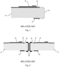
Multi-ink layered printed electrode for wrap around electrodes
PatentPendingUS20240322101A1
Innovation
- A multi-layer electrode printing process using a combination of metal precursor ink and nanoparticle ink, where the metal precursor ink establishes good electrical contact and low contact resistance, and the nanoparticle ink reduces line resistance, with consolidation at low temperatures to fuse metals and remove organic coatings, enhancing adhesion and electrical continuity.
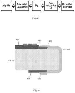
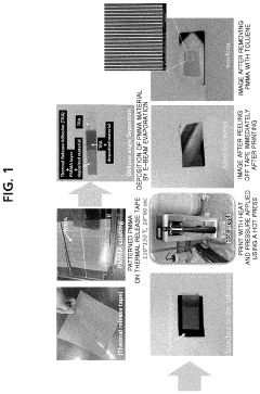
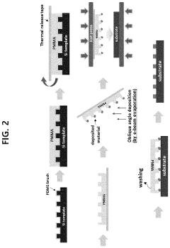
Method of printing nanostructure
PatentPendingUS20240103362A1
Innovation
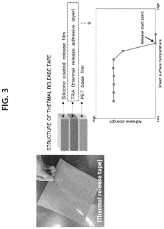
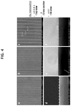
- A method involving a template substrate with a formed pattern, a polymer thin film coated with a thermal release tape, and functional material deposition on a replica pattern, followed by heat and pressure application to weaken adhesive forces and facilitate easy, large-scale printing of nanostructures on various substrates.
Sustainability Aspects of Printed Nanoelectronics
The environmental impact of printed nanoelectronics represents a critical dimension in evaluating the sustainability of low-cost printing methods for nanostructured electrodes. These emerging technologies offer significant advantages over traditional manufacturing processes, particularly in terms of resource efficiency and waste reduction. The additive nature of printing techniques minimizes material consumption by depositing functional materials only where needed, contrasting sharply with conventional subtractive manufacturing approaches that generate substantial waste.
Energy consumption patterns in printed nanoelectronics demonstrate promising sustainability metrics. Roll-to-roll and inkjet printing processes operate at lower temperatures and require less energy compared to vacuum-based deposition methods commonly used in traditional electronics manufacturing. Recent studies indicate energy savings of up to 60% when implementing solution-based printing techniques for electrode fabrication, contributing to reduced carbon footprints across the production lifecycle.
Material selection plays a pivotal role in the environmental profile of printed nanoelectrodes. Water-based and bio-derived inks are increasingly replacing solvent-based alternatives, significantly reducing volatile organic compound (VOC) emissions. Additionally, research into biodegradable substrates and conductive materials extracted from renewable resources is advancing rapidly, with cellulose-based substrates and carbon-derived from biomass showing particular promise for environmentally responsible electrode production.
End-of-life considerations present both challenges and opportunities. The composite nature of printed electronics can complicate recycling processes, yet their thin-film architecture typically utilizes smaller quantities of critical materials compared to conventional electronics. Innovative approaches to design for disassembly and material recovery are emerging, with selective dissolution techniques enabling the separation and reclamation of valuable nanomaterials from printed electrodes.
Lifecycle assessment (LCA) studies comparing printed nanoelectrodes with conventional manufacturing reveal complex sustainability tradeoffs. While printed methods generally demonstrate advantages in manufacturing-phase environmental impacts, the durability and longevity of these products remain critical factors in determining their overall ecological footprint. Recent advancements in encapsulation technologies are addressing these concerns, extending the functional lifespan of printed nanoelectrodes in various applications.
Regulatory frameworks worldwide are increasingly incorporating sustainability metrics into manufacturing standards, creating both compliance challenges and market opportunities for printed nanoelectronics. Companies adopting green chemistry principles and circular economy approaches in their production processes are gaining competitive advantages through reduced compliance costs and enhanced brand positioning in environmentally conscious markets.
Cost-Performance Analysis of Printing Methods
The economic viability of nanostructured electrode printing methods hinges on the delicate balance between production costs and performance outcomes. Screen printing emerges as the most cost-effective solution, with equipment investments ranging from $5,000 to $20,000 and operational costs of $0.05-0.15 per electrode. This method delivers moderate resolution (50-100 μm) and throughput (300-500 units/hour), making it ideal for large-scale commercial applications where extreme precision is not paramount.
Inkjet printing presents a middle-ground option with equipment costs between $15,000 and $50,000 and per-electrode costs of $0.10-0.30. The technology offers improved resolution (20-50 μm) compared to screen printing, with moderate throughput (150-300 units/hour). The higher initial investment is often justified in applications requiring greater precision without sacrificing production volume.
At the premium end, aerosol jet printing demands substantial capital expenditure ($100,000-500,000) with operational costs of $0.50-2.00 per electrode. However, this method delivers superior resolution (10-20 μm) and enables complex geometries unattainable with other techniques. Despite lower throughput (50-150 units/hour), aerosol jet printing remains valuable for high-performance, specialized applications where performance outweighs cost considerations.
Electrohydrodynamic printing represents an emerging technology with promising cost-performance metrics. Equipment costs ($30,000-80,000) and operational expenses ($0.20-0.60 per electrode) position it between inkjet and aerosol methods, while offering exceptional resolution (5-10 μm) and moderate throughput (100-200 units/hour). This method shows particular promise for bridging the gap between mass production and high-precision requirements.
Material selection significantly impacts both cost and performance across all printing methods. Conventional materials like silver nanoparticle inks cost $300-500 per liter but offer excellent conductivity (1-3 × 10^7 S/m). Alternative carbon-based inks reduce material costs to $100-300 per liter while sacrificing some conductivity (1-5 × 10^5 S/m). Recent developments in copper-based formulations ($150-350 per liter) are approaching silver's performance (0.5-1 × 10^7 S/m) at substantially lower costs.
The total cost of ownership analysis reveals that high-volume production scenarios favor screen printing, with costs decreasing to $0.03-0.08 per electrode at scale. Conversely, specialized applications requiring precision features benefit from aerosol or electrohydrodynamic methods despite higher unit costs, as these technologies enable performance characteristics that translate to superior end-product functionality and potentially higher market value.
Unlock deeper insights with Patsnap Eureka Quick Research — get a full tech report to explore trends and direct your research. Try now!
Generate Your Research Report Instantly with AI Agent
Supercharge your innovation with Patsnap Eureka AI Agent Platform!