Environmental Monitoring Networks Using Nanostructured Sensors
AUG 28, 202510 MIN READ
Generate Your Research Report Instantly with AI Agent
Patsnap Eureka helps you evaluate technical feasibility & market potential.
Nanostructured Sensor Technology Evolution and Objectives
Nanostructured sensors have evolved significantly over the past three decades, transforming from laboratory curiosities to essential components in modern environmental monitoring systems. The initial development phase in the 1990s focused primarily on basic material science, exploring how nanoscale structures could enhance sensing capabilities through increased surface-to-volume ratios. By the early 2000s, researchers had established fundamental principles for creating sensors with nanomaterials such as carbon nanotubes, metal oxide nanoparticles, and quantum dots, demonstrating superior sensitivity compared to conventional sensing technologies.
The mid-2000s marked a critical transition from theoretical research to practical applications, with significant breakthroughs in fabrication techniques enabling more consistent production of nanostructured sensors. Advances in lithography, chemical vapor deposition, and sol-gel processes facilitated the creation of increasingly complex and functional nanostructured sensing elements. This period also saw the integration of multiple sensing modalities into single platforms, allowing for the detection of various environmental parameters simultaneously.
From 2010 onwards, the focus shifted toward addressing key challenges in field deployment, including power consumption, durability in harsh environments, and long-term stability. Innovations in self-healing materials, energy harvesting technologies, and protective encapsulation methods have progressively enhanced the robustness of nanostructured sensors for real-world environmental monitoring applications. The miniaturization trend has continued, with sensors becoming smaller while maintaining or improving their performance characteristics.
The current technological landscape is characterized by the convergence of nanostructured sensors with wireless communication technologies, artificial intelligence, and edge computing. This integration enables the creation of sophisticated environmental monitoring networks capable of real-time data collection, processing, and analysis across diverse geographical locations. Recent developments have also emphasized sustainability, with research focusing on biodegradable nanomaterials and reduced environmental footprints.
The primary objectives for nanostructured sensor technology in environmental monitoring networks include achieving unprecedented detection limits for pollutants and contaminants, particularly those present at trace concentrations that conventional sensors cannot reliably detect. There is also a strong focus on developing multi-parameter sensing capabilities that can simultaneously monitor various environmental indicators, providing a more comprehensive assessment of ecosystem health. Additional goals include extending operational lifetimes in field conditions, reducing costs to enable widespread deployment, and creating standardized interfaces for seamless integration with existing environmental monitoring infrastructure.
Market Analysis for Environmental Monitoring Solutions
The global environmental monitoring market is experiencing robust growth, driven by increasing environmental concerns, stringent regulatory frameworks, and technological advancements in sensing capabilities. The market was valued at approximately $19.9 billion in 2021 and is projected to reach $30.7 billion by 2026, representing a compound annual growth rate (CAGR) of 9.1%. This growth trajectory is particularly pronounced in the nanostructured sensor segment, which is revolutionizing environmental monitoring networks through enhanced sensitivity, selectivity, and miniaturization capabilities.
Demand for environmental monitoring solutions is primarily fueled by escalating pollution levels across urban centers, industrial zones, and agricultural regions. Air quality monitoring represents the largest market segment, accounting for roughly 35% of the total market share, followed by water quality monitoring at 28% and soil contamination detection at 18%. The remaining market share is distributed among noise pollution, radiation detection, and other specialized monitoring applications.
Geographically, North America currently dominates the market with approximately 32% share, followed closely by Europe at 29% and Asia-Pacific at 27%. However, the Asia-Pacific region is expected to witness the highest growth rate of 11.3% during the forecast period, primarily due to rapid industrialization, urbanization, and increasing environmental awareness in countries like China and India.
Industry-specific demand patterns reveal that government and regulatory bodies constitute the largest end-user segment (41%), followed by industrial enterprises (27%), commercial establishments (18%), and residential applications (14%). The industrial sector, particularly manufacturing, chemical processing, and power generation, demonstrates the strongest growth potential due to increasingly stringent emission standards and corporate sustainability initiatives.
The integration of nanostructured sensors into environmental monitoring networks is creating significant market opportunities. These advanced sensing technologies offer substantial improvements in detection limits, enabling the identification of pollutants at parts-per-billion or even parts-per-trillion levels. This capability is particularly valuable for detecting emerging contaminants of concern, including pharmaceutical residues, microplastics, and novel industrial chemicals.
Consumer trends indicate growing demand for real-time, continuous monitoring solutions that provide actionable insights rather than periodic sampling data. This shift is driving the development of integrated monitoring networks that combine nanostructured sensors with wireless connectivity, cloud computing, and advanced analytics. The market for such integrated solutions is growing at 13.2% annually, significantly outpacing the overall market growth rate.
Global Status and Technical Barriers in Nanostructured Sensing
The global landscape of nanostructured sensing for environmental monitoring presents a complex picture of advancement and limitation. Currently, developed regions such as North America, Western Europe, and East Asia lead in research and deployment of nanostructured sensor networks. The United States maintains dominance through substantial investments from agencies like the EPA and NSF, while the European Union has established comprehensive frameworks through initiatives like Horizon Europe specifically targeting environmental nanotechnology applications.
In Asia, Japan and South Korea have achieved significant breakthroughs in miniaturization and energy efficiency of nanostructured sensors, while China has rapidly expanded its research capacity, particularly in graphene-based sensing technologies. However, developing regions face considerable implementation gaps due to limited infrastructure and financial constraints, despite often experiencing more severe environmental challenges.
Technical barriers in nanostructured sensing remain substantial despite progress. Sensor stability presents a primary challenge, as nanomaterials frequently exhibit performance degradation when exposed to harsh environmental conditions over extended periods. Many promising laboratory prototypes fail to maintain sensitivity and selectivity when deployed in real-world settings with variable temperature, humidity, and contaminant exposure.
Power consumption represents another significant hurdle, particularly for remote deployment scenarios. While energy harvesting technologies show promise, current solutions often fail to provide sufficient power for continuous operation of sensor networks in field conditions. This limitation severely restricts the deployment scope of comprehensive monitoring networks.
Standardization issues further complicate advancement, with inconsistent calibration methodologies and lack of universal performance metrics hampering comparative analysis and regulatory acceptance. The absence of standardized testing protocols specifically designed for nanomaterial-based environmental sensors creates significant barriers to commercial adoption and regulatory approval.
Manufacturing scalability presents additional challenges, as many laboratory-developed nanostructured sensors rely on fabrication techniques that prove difficult to scale economically. The precision required for consistent nanomaterial production often results in high unit costs and yield variability, limiting widespread implementation.
Data integration capabilities also remain underdeveloped, with many current systems lacking effective mechanisms to process, analyze, and interpret the massive data streams generated by distributed sensor networks. This deficiency significantly reduces the practical utility of even technically advanced sensing systems in environmental management applications.
Current Nano-Sensing Network Architectures and Implementations
01 Carbon nanotube-based sensors
Carbon nanotubes are utilized in sensor development due to their unique electrical, mechanical, and chemical properties. These nanostructured materials can be functionalized to detect specific analytes with high sensitivity. The carbon nanotube architecture provides excellent electron transfer capabilities and large surface area, making them ideal for various sensing applications including gas detection, biomolecule sensing, and environmental monitoring.- Nanostructured materials for gas sensing applications: Nanostructured materials such as metal oxides and carbon-based nanomaterials are utilized in gas sensing applications due to their high surface area and enhanced sensitivity. These materials can detect various gases through changes in electrical conductivity when gas molecules interact with their surface. The nanostructured design allows for improved response time, selectivity, and lower detection limits compared to conventional sensors.
- Fabrication methods for nanostructured sensor devices: Various fabrication techniques are employed to create nanostructured sensors, including chemical vapor deposition, sol-gel processing, and lithographic methods. These processes enable precise control over the size, shape, and composition of nanostructures, which directly affects sensor performance. Advanced manufacturing approaches allow for the integration of nanostructures into functional devices with reproducible sensing characteristics.
- Nanostructured electrochemical sensors: Electrochemical sensors utilizing nanostructured materials offer enhanced sensitivity for detecting biological and chemical analytes. These sensors leverage the unique electrical properties of nanomaterials to improve electron transfer rates and signal amplification. The high surface-to-volume ratio of nanostructures provides more active sites for electrochemical reactions, resulting in lower detection limits and wider dynamic ranges.
- Optical and photonic nanostructured sensors: Nanostructured optical sensors utilize phenomena such as surface plasmon resonance, photoluminescence, and light scattering for detection purposes. These sensors incorporate nanomaterials that interact with light in specific ways when exposed to target analytes. The optical properties of nanostructures can be tuned by controlling their size, shape, and composition, enabling highly sensitive and selective detection methods for various applications.
- Flexible and wearable nanostructured sensors: Flexible and wearable sensor platforms incorporate nanostructured materials on substrates that can conform to curved surfaces, including human skin. These sensors combine nanomaterials with flexible polymers or textiles to create devices that can monitor physiological parameters, environmental conditions, or movement in real-time. The integration of nanostructures with flexible electronics enables new applications in healthcare monitoring, sports performance analysis, and environmental sensing.
02 Nanowire sensor technologies
Nanowire-based sensors leverage the high surface-to-volume ratio of nanowires to achieve enhanced sensitivity and selectivity. These nanostructured sensors can detect minute changes in electrical properties when target molecules interact with their surface. Various materials including silicon, zinc oxide, and metal oxides are used to fabricate nanowires for sensing applications in healthcare, environmental monitoring, and security systems.Expand Specific Solutions03 Nanoparticle-based sensing platforms
Nanoparticles are incorporated into sensing platforms to enhance detection capabilities through optical, electrochemical, or magnetic transduction mechanisms. These nanostructured sensors utilize the unique properties of nanoparticles such as quantum dots, gold nanoparticles, and magnetic nanoparticles to achieve high sensitivity and specificity. Applications include point-of-care diagnostics, chemical detection, and biological sensing.Expand Specific Solutions04 Flexible and wearable nanostructured sensors
Flexible and wearable sensor technologies incorporate nanostructured materials into substrates that can conform to various surfaces, including human skin. These sensors combine nanomaterials with flexible electronics to create devices capable of continuous monitoring of physiological parameters, environmental conditions, or structural health. The integration of nanomaterials enhances sensitivity while maintaining mechanical flexibility for comfortable wearable applications.Expand Specific Solutions05 Nanocomposite sensing materials
Nanocomposites combine nanomaterials with polymers or other matrices to create sensing materials with enhanced properties. These hybrid materials leverage the synergistic effects between the nanoscale components and the matrix to improve sensitivity, selectivity, and stability. Nanocomposite sensors find applications in gas sensing, strain detection, temperature monitoring, and chemical analysis, offering advantages such as improved mechanical properties and processing capabilities.Expand Specific Solutions
Industry Leaders in Nanostructured Environmental Sensors
Environmental monitoring networks using nanostructured sensors are currently in an early growth phase, characterized by rapid technological advancement and expanding market applications. The global market for these systems is projected to reach $3-5 billion by 2027, driven by increasing environmental concerns and regulatory requirements. From a technological maturity perspective, key players demonstrate varying levels of development: academic institutions (University of California, MIT, University of Maryland) are pioneering fundamental research; government agencies (NIST) are establishing standards; while commercial entities like Analog Devices, Nanomix, and AerNos are transitioning from R&D to commercialization. Companies such as IBM and Bosch are leveraging their extensive resources to integrate these sensors into comprehensive IoT environmental monitoring solutions, while specialized firms like NanoLab are focusing on point-of-care applications with environmental crossover potential.
Nanomix, Inc.
Technical Solution: Nanomix has pioneered carbon nanotube (CNT) based nanostructured sensors for environmental monitoring networks. Their proprietary technology platform combines carbon nanotubes with specialized polymer matrices to create highly sensitive and selective chemical sensors. The company's environmental monitoring solution features a distributed network architecture where individual sensor nodes communicate wirelessly to central hubs. Each sensor incorporates multiple sensing elements with different functionalization schemes to detect various environmental pollutants and parameters. Nanomix's sensors operate on electrochemical principles, measuring conductivity changes when target molecules interact with the functionalized nanotubes. The company has developed specialized surface chemistry modifications that enhance selectivity for specific environmental contaminants while minimizing interference[2]. Their sensors demonstrate remarkable stability in field conditions, with proprietary encapsulation techniques protecting the sensitive nanomaterials from environmental degradation while maintaining rapid response characteristics.
Strengths: Exceptional sensitivity at room temperature operation; minimal power requirements suitable for remote deployment; proven stability in field conditions; established manufacturing processes for consistent sensor production. Weaknesses: Higher initial cost compared to conventional sensors; requires periodic recalibration in highly variable environments; limited to specific target analytes per sensor configuration.
Agilent Technologies, Inc.
Technical Solution: Agilent Technologies has developed sophisticated environmental monitoring networks utilizing their proprietary nanostructured sensor technology. Their approach combines multiple sensing modalities including surface-enhanced Raman spectroscopy (SERS) with nanostructured substrates for molecular identification, electrochemical sensors with nanoengineered electrodes for trace metal detection, and functionalized nanomaterials for volatile organic compound (VOC) monitoring. Agilent's environmental monitoring platform features a distributed architecture where specialized sensor nodes are deployed based on site-specific requirements. Their sensors incorporate gold nanoparticle-enhanced surfaces that dramatically increase detection sensitivity through localized surface plasmon resonance effects. The company has developed comprehensive data management systems that integrate with their sensor networks, providing automated calibration, quality control, and regulatory compliance features[6][8]. Agilent's technology enables real-time detection of environmental contaminants at concentrations orders of magnitude lower than conventional methods, with laboratory-grade accuracy in field deployments.
Strengths: Exceptional analytical performance approaching laboratory instrumentation quality; comprehensive data management and quality control systems; established calibration protocols ensuring measurement traceability; robust design for industrial environments. Weaknesses: Higher cost than simpler monitoring solutions; greater complexity requiring trained personnel for optimal operation; larger form factor than some competing nanosensor technologies; higher power requirements limiting deployment options.
Breakthrough Patents in Nanostructured Environmental Monitoring
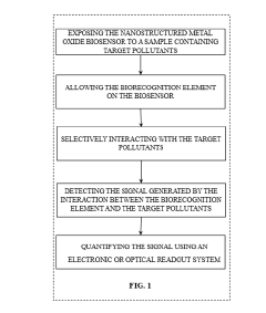
Nanostructured metal oxide biosensors for environmental monitoring and pollution detection
PatentPendingIN202321062493A
Innovation
- Nanostructured metal oxide biosensors, comprising materials like zinc oxide, titanium dioxide, or tin dioxide in nanoparticle, nanowire, or nanosheet forms, integrated with biorecognition elements such as enzymes, antibodies, or DNA probes, and electronic or optical readout systems for enhanced sensitivity and selectivity in pollutant detection.
Nanostructured sensor architecture and method for enhanced chemical detection
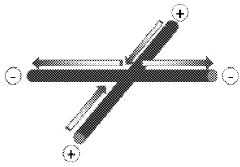
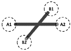
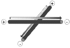
PatentInactiveUS20160054258A1
Innovation
- A carbon nanotube (CNT) sensor network with electrical anisotropy, featuring a plurality of CNTs arranged to form networks with different junction densities in orthogonal directions, allowing for dynamic measurement of electrical characteristics under various stimuli, including chemical species presence, through application of electrical signals and secondary modulators.
Sustainability Impact and Green Technology Integration
The integration of nanostructured sensors into environmental monitoring networks represents a significant advancement in green technology with far-reaching sustainability impacts. These sophisticated sensing systems contribute substantially to environmental conservation efforts by enabling precise, real-time detection of pollutants at previously undetectable concentrations, allowing for immediate remediation actions before ecological damage becomes severe.
Nanostructured sensor networks dramatically reduce the resource footprint of traditional environmental monitoring approaches. Their minimal energy requirements—often powered by renewable sources such as solar or kinetic energy harvesting—represent a paradigm shift from conventional power-intensive monitoring equipment. Additionally, the miniaturization of these sensors significantly decreases material consumption in manufacturing while extending operational lifespans through enhanced durability against environmental stressors.
The lifecycle sustainability of these monitoring networks is particularly noteworthy. Many advanced nanostructured sensors incorporate biodegradable components or recyclable materials, addressing end-of-life environmental concerns. This characteristic aligns with circular economy principles, reducing electronic waste that typically plagues environmental technology deployments.
From a broader ecological perspective, these monitoring networks enable unprecedented insights into ecosystem health and biodiversity conservation. By tracking subtle environmental changes with extraordinary sensitivity, they provide early warning systems for habitat degradation, allowing for proactive conservation measures rather than reactive responses to environmental crises.
The economic sustainability dimension cannot be overlooked. While initial deployment costs may exceed traditional monitoring methods, the long-term operational efficiency and maintenance savings create compelling total cost of ownership advantages. Furthermore, these networks generate high-quality environmental data that holds significant value for research institutions, regulatory bodies, and commercial enterprises, creating new green economy opportunities.
In urban environments, nanostructured sensor networks contribute to sustainable city initiatives by optimizing resource management. Water quality monitoring systems employing these sensors enable precise treatment protocols, reducing chemical usage while ensuring safety standards. Similarly, air quality monitoring networks inform traffic management and industrial emission controls, supporting public health while minimizing unnecessary restrictions on economic activity.
The democratization of environmental data through these networks also advances social sustainability goals. By making sophisticated environmental monitoring accessible to communities previously excluded from such technology, these systems empower citizen science initiatives and enhance environmental justice through transparent, verifiable pollution tracking in vulnerable communities.
Data Management and AI Analytics for Nano-Sensor Networks
The integration of advanced data management systems with artificial intelligence analytics represents a critical component for maximizing the effectiveness of environmental monitoring networks based on nanostructured sensors. These networks generate massive volumes of heterogeneous data that require sophisticated processing frameworks to extract actionable insights. Current data management approaches employ distributed database architectures that facilitate real-time data collection from geographically dispersed nano-sensor arrays while maintaining data integrity across challenging environmental conditions.
Edge computing has emerged as a pivotal technology in this domain, enabling preliminary data processing directly at sensor nodes to reduce transmission bandwidth requirements and power consumption. This approach is particularly valuable for remote environmental monitoring applications where connectivity may be intermittent. Hierarchical data storage systems that implement automated data classification protocols ensure efficient organization of sensor readings according to environmental parameters, temporal patterns, and anomaly indicators.
Machine learning algorithms specifically optimized for nano-sensor data have demonstrated remarkable capabilities in pattern recognition across environmental datasets. Convolutional neural networks (CNNs) excel at identifying spatial correlations in pollution dispersion patterns, while recurrent neural networks (RNNs) and Long Short-Term Memory (LSTM) architectures effectively capture temporal dynamics in environmental parameters. These AI models can detect subtle environmental changes that might escape traditional analytical methods, providing early warning capabilities for emerging environmental threats.
Transfer learning techniques have proven particularly valuable in environmental monitoring applications, allowing models trained on data-rich environments to be adapted for deployment in regions with limited historical data. This approach significantly reduces the training data requirements for new monitoring installations while maintaining high analytical accuracy. Federated learning frameworks further enhance this capability by enabling collaborative model training across multiple sensor networks without centralizing sensitive environmental data.
Explainable AI (XAI) methodologies are increasingly incorporated into environmental monitoring analytics to ensure transparency in decision-making processes. This is especially important when sensor data informs regulatory compliance or public health interventions. Recent advances in quantum computing show promise for processing complex environmental models that integrate nano-sensor data with atmospheric, hydrological, and ecological parameters at unprecedented scales.
The convergence of blockchain technology with environmental monitoring networks offers enhanced data provenance tracking and tamper-proof audit trails for regulatory compliance. Smart contracts can automate response protocols when predefined environmental thresholds are breached, triggering mitigation measures without human intervention. As these technologies mature, we anticipate the development of increasingly autonomous environmental monitoring systems capable of self-calibration, adaptive sampling rates, and predictive maintenance based on AI-driven analytics.
Unlock deeper insights with Patsnap Eureka Quick Research — get a full tech report to explore trends and direct your research. Try now!
Generate Your Research Report Instantly with AI Agent
Supercharge your innovation with Patsnap Eureka AI Agent Platform!