Electrolytic Cell Use in the Purification of Semiconductor Materials
AUG 1, 20259 MIN READ
Generate Your Research Report Instantly with AI Agent
Patsnap Eureka helps you evaluate technical feasibility & market potential.
Electrolytic Purification Background and Objectives
Electrolytic purification has emerged as a critical process in the semiconductor industry, playing a pivotal role in the production of high-purity materials essential for advanced electronic devices. The background of this technology dates back to the early 20th century when electrochemistry principles were first applied to material refinement. However, its significance in semiconductor purification has grown exponentially with the increasing demand for ultra-pure materials in the digital age.
The evolution of electrolytic purification techniques has been closely tied to the rapid advancement of semiconductor technology. As Moore's Law continues to drive the miniaturization of electronic components, the need for materials with impurity levels in the parts per billion (ppb) or even parts per trillion (ppt) range has become paramount. This has led to continuous refinement and innovation in electrolytic cell design and operation.
The primary objective of electrolytic purification in semiconductor materials is to achieve unprecedented levels of purity, removing trace contaminants that can significantly impact device performance and reliability. This process aims to eliminate metallic impurities, dopants, and other unwanted elements that can introduce defects or alter the electrical properties of semiconductors.
Another crucial goal is to develop scalable and cost-effective purification methods that can meet the growing demand for high-purity semiconductor materials. As the global semiconductor market expands, there is an increasing need for efficient purification processes that can be implemented on an industrial scale without compromising on quality or yield.
Furthermore, electrolytic purification techniques are being developed with sustainability in mind. The semiconductor industry is under pressure to reduce its environmental footprint, and purification processes are no exception. Objectives include minimizing energy consumption, reducing waste generation, and exploring the use of more environmentally friendly electrolytes and electrode materials.
Research and development efforts are also focused on expanding the range of materials that can be purified using electrolytic methods. While silicon remains the dominant semiconductor material, the industry is increasingly exploring alternatives such as gallium nitride, silicon carbide, and various III-V compounds. Adapting electrolytic purification techniques to these materials presents both challenges and opportunities for innovation.
In conclusion, the background and objectives of electrolytic cell use in semiconductor material purification reflect a dynamic field driven by the relentless pursuit of higher purity, greater efficiency, and enhanced sustainability. As the semiconductor industry continues to evolve, electrolytic purification techniques are expected to play an increasingly critical role in enabling the next generation of electronic devices and technologies.
Semiconductor Industry Demand Analysis
The semiconductor industry's demand for high-purity materials has been steadily increasing, driven by the continuous advancement of semiconductor technology and the growing complexity of integrated circuits. As device dimensions shrink and performance requirements become more stringent, the need for ultra-pure semiconductor materials has become paramount. This demand extends beyond traditional silicon to include compound semiconductors and other advanced materials.
The global semiconductor market has been experiencing robust growth, with projections indicating a compound annual growth rate (CAGR) of over 7% in the coming years. This growth is fueled by emerging technologies such as 5G, artificial intelligence, Internet of Things (IoT), and autonomous vehicles, all of which rely heavily on advanced semiconductor components. Consequently, the demand for high-purity semiconductor materials is expected to outpace the overall market growth.
Electrolytic cell purification plays a crucial role in meeting this demand by providing a cost-effective and efficient method for producing high-purity semiconductor materials. The market for electrolytic purification equipment and services is anticipated to grow significantly, with a particular focus on applications in silicon, gallium arsenide, and other compound semiconductors.
The increasing emphasis on environmental sustainability and energy efficiency in semiconductor manufacturing has also contributed to the rising demand for electrolytic purification methods. These processes often offer lower energy consumption and reduced chemical waste compared to traditional purification techniques, aligning with the industry's goals for greener production practices.
Geographically, the demand for electrolytic cell purification in semiconductor materials is most pronounced in regions with strong semiconductor manufacturing bases. East Asia, particularly Taiwan, South Korea, and Japan, leads in demand due to their dominant position in chip production. China's rapidly expanding semiconductor industry is also driving significant growth in the demand for purification technologies.
The automotive sector's shift towards electric vehicles and advanced driver assistance systems (ADAS) is creating new opportunities for semiconductor materials, further boosting the demand for high-purity components. This trend is expected to accelerate as automotive electrification gains momentum globally.
In conclusion, the semiconductor industry's demand for electrolytic cell purification in semiconductor materials is robust and multifaceted. It is driven by technological advancements, market growth, environmental concerns, and emerging applications across various sectors. As the industry continues to evolve, the importance of high-purity materials will only increase, solidifying the critical role of electrolytic purification technologies in the semiconductor supply chain.
Current Challenges in Electrolytic Purification
Despite significant advancements in electrolytic purification techniques for semiconductor materials, several challenges persist in achieving optimal results. One of the primary issues is the control of impurity levels during the purification process. Even trace amounts of contaminants can significantly impact the performance of semiconductor devices, making it crucial to achieve ultra-high purity levels consistently.
The complexity of electrolyte composition poses another challenge. Balancing the electrolyte solution to effectively remove specific impurities while maintaining the desired properties of the semiconductor material requires precise control and continuous monitoring. This becomes particularly challenging when dealing with novel semiconductor compounds or when targeting the removal of multiple impurity types simultaneously.
Energy efficiency remains a concern in electrolytic purification processes. The high power consumption associated with maintaining the necessary current densities and voltages for effective purification can lead to increased production costs and environmental impact. Developing more energy-efficient electrolytic cell designs and optimizing process parameters are ongoing challenges in the field.
Scaling up electrolytic purification processes for industrial-scale production presents additional hurdles. Maintaining uniform current distribution and electrolyte flow across larger electrolytic cells is critical for ensuring consistent purification results. However, achieving this uniformity becomes increasingly difficult as the size of the cells increases, potentially leading to variations in purity levels across the processed material.
The formation of unwanted byproducts during electrolysis is another significant challenge. These byproducts can interfere with the purification process, potentially recontaminating the semiconductor material or altering its properties. Developing strategies to minimize byproduct formation or efficiently remove them from the system is crucial for improving overall purification efficiency.
Electrode degradation and contamination over time can also impact the long-term performance and reliability of electrolytic purification systems. Finding electrode materials and designs that can withstand the harsh electrolytic environment while maintaining their effectiveness in impurity removal is an ongoing area of research and development.
Lastly, the need for real-time monitoring and control of the purification process presents technological challenges. Developing sensitive and reliable in-situ measurement techniques for impurity levels and electrolyte composition is essential for optimizing the purification process and ensuring consistent product quality. Integrating these monitoring systems with advanced control algorithms to enable real-time adjustments remains a complex task in industrial settings.
Existing Electrolytic Cell Purification Methods
01 Electrolytic cell design for purification
Specialized electrolytic cell designs are employed for efficient purification processes. These designs may include specific electrode configurations, membrane separators, or innovative cell structures to enhance the separation and purification of target substances.- Electrolytic cell design for purification: Specialized electrolytic cell designs are employed for purification processes. These designs may include specific electrode configurations, membrane separators, or innovative cell structures to enhance the efficiency of the purification process. The cells are optimized for various applications such as water treatment, metal recovery, or chemical synthesis.
- Electrochemical treatment of water and wastewater: Electrolytic cells are used for the purification of water and wastewater. This process involves the removal of contaminants, disinfection, and treatment of industrial effluents. The electrolytic treatment can effectively remove organic pollutants, heavy metals, and pathogens from water sources.
- Metal recovery and purification: Electrolytic cells are utilized for the recovery and purification of metals from various sources, including ores, industrial waste, and recycled materials. This process involves the selective deposition of metals onto cathodes, allowing for the separation and purification of different metal species.
- Electrolytic purification of organic compounds: Electrolytic cells are employed for the purification of organic compounds in chemical and pharmaceutical industries. This process can involve the removal of impurities, isomerization, or selective oxidation/reduction of organic molecules to obtain high-purity products.
- Advanced electrode materials for electrolytic purification: Development of advanced electrode materials to enhance the efficiency and selectivity of electrolytic purification processes. These materials may include nanostructured electrodes, catalytic coatings, or composite materials designed to improve the performance of electrolytic cells in various purification applications.
02 Membrane technology in electrolytic purification
Advanced membrane technologies are integrated into electrolytic cells to improve selectivity and efficiency in purification processes. These membranes can facilitate ion exchange, separate specific compounds, or prevent unwanted reactions during electrolysis.Expand Specific Solutions03 Electrode materials for enhanced purification
Specialized electrode materials are developed to improve the efficiency and selectivity of electrolytic purification processes. These materials may have catalytic properties, increased surface area, or specific compositions tailored to the target substances being purified.Expand Specific Solutions04 Control systems for electrolytic purification
Advanced control systems are implemented to optimize the electrolytic purification process. These systems may include sensors, feedback mechanisms, and automated adjustments to maintain optimal conditions for purification, such as pH, temperature, and current density.Expand Specific Solutions05 Electrolytic purification of specific substances
Tailored electrolytic purification processes are developed for specific substances or applications. These may include purification of metals, treatment of wastewater, desalination of water, or removal of contaminants from industrial processes.Expand Specific Solutions
Key Players in Electrolytic Cell Technology
The electrolytic cell purification of semiconductor materials is in a mature stage of development, with a substantial global market driven by the growing demand for high-purity semiconductors in electronics. The technology's maturity is evident from the involvement of established players like Renesas Electronics Corp. and Robert Bosch GmbH, which have extensive experience in semiconductor manufacturing. However, the field continues to evolve, with research institutions such as the Dalian Institute of Chemical Physics and Arizona State University contributing to advancements. The competitive landscape is diverse, including both large corporations and specialized firms like Semiconductor Energy Laboratory Co., Ltd., indicating ongoing innovation and market opportunities in this critical area of semiconductor production.
Dalian Institute of Chemical Physics Chinese Academy of Sci
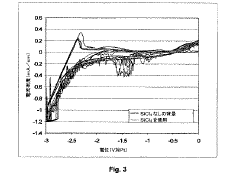
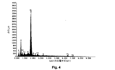
Technical Solution: The Dalian Institute of Chemical Physics has pioneered a novel electrolytic cell design for semiconductor material purification, focusing on compound semiconductors such as gallium arsenide and indium phosphide. Their approach utilizes a pulsed electrochemical technique combined with a rotating disk electrode system, which enhances mass transfer and allows for more uniform purification across the material [2]. The institute has also developed a proprietary electrolyte formulation that selectively removes specific impurities while minimizing damage to the semiconductor crystal structure. This method has demonstrated the ability to reduce impurity concentrations to parts per billion levels, particularly effective for removing transition metal contaminants [4]. Additionally, the process incorporates a closed-loop recycling system for the electrolyte, improving sustainability and reducing operational costs.
Strengths: Highly effective for compound semiconductors, environmentally friendly due to electrolyte recycling. Weaknesses: May require specialized equipment and expertise to operate effectively.
Renesas Electronics Corp.
Technical Solution: Renesas Electronics Corp. has developed a proprietary electrolytic purification system specifically tailored for silicon carbide (SiC) semiconductor materials. Their technology employs a high-temperature molten salt electrolysis process, which allows for the removal of both metallic and non-metallic impurities from SiC wafers and bulk crystals [5]. The system utilizes a unique electrode configuration that promotes uniform current distribution across the material, ensuring consistent purification. Renesas has also implemented advanced process control algorithms that adjust electrolysis parameters based on material resistivity measurements, optimizing the purification efficiency for different grades of SiC [6]. This technology has enabled Renesas to produce high-quality SiC materials for power electronics applications, with defect densities reduced by up to 70% compared to conventional purification methods.
Strengths: Specialized for SiC purification, enabling high-quality materials for power electronics. Advanced process control for optimized efficiency. Weaknesses: Limited applicability to other semiconductor materials, potentially high initial investment costs.
Innovations in Electrolytic Cell Design
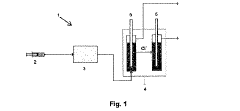
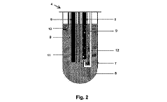
Method for purifying semiconductor material by utilizing redox reaction
PatentInactiveJP2009535515A
Innovation
- A method involving redox reactions in an electrolytic cell where impure silicon is oxidized to silicon halides at the anode and reduced to pure silicon at the cathode, using ionic compounds instead of gaseous reactants, leveraging reversible reactions to minimize energy input and simplify equipment requirements.
Method and apparatus for applying electrical charge through a liquid having enhanced suspension properties
PatentInactiveEP2376127A1
Innovation
- An apparatus and method that treat a liquid with compounds like surfactants or zeolites to enhance suspension properties, coupled with an electrolysis cell to produce electrochemically activated liquids, and an electroporation electrode to generate an alternating electric field, creating a conductive path for microorganism destruction.
Environmental Impact of Electrolytic Processes
The use of electrolytic cells in the purification of semiconductor materials has significant environmental implications that warrant careful consideration. These processes, while essential for producing high-purity materials crucial to the semiconductor industry, can have both positive and negative impacts on the environment.
One of the primary environmental concerns associated with electrolytic purification is the consumption of energy. The process typically requires substantial electrical power, which, depending on the energy source, can contribute to greenhouse gas emissions and other forms of pollution. However, advancements in energy-efficient electrolytic cell designs and the increasing use of renewable energy sources in semiconductor manufacturing facilities are helping to mitigate these impacts.
Water usage and wastewater management are also critical environmental factors. Electrolytic purification often involves large volumes of water, both as a medium for the electrolytic process and for cooling purposes. The resulting wastewater may contain trace amounts of semiconductor materials, acids, and other chemicals used in the purification process. Proper treatment and recycling of this wastewater are essential to prevent contamination of local water sources and ecosystems.
The production and disposal of waste materials from electrolytic processes present another environmental challenge. Spent electrolytes, electrode materials, and other byproducts must be carefully managed to prevent the release of potentially harmful substances into the environment. Many semiconductor manufacturers have implemented comprehensive waste management programs, including recycling initiatives for valuable materials and proper disposal methods for hazardous waste.
On the positive side, electrolytic purification can contribute to environmental sustainability by enabling the production of more efficient semiconductor devices. These high-purity materials are essential for developing advanced technologies such as solar cells, LED lighting, and energy-efficient electronics, which can help reduce overall energy consumption and environmental impact in various sectors.
Furthermore, the precision of electrolytic purification methods can lead to reduced material waste compared to other purification techniques. This efficiency in material use translates to lower resource extraction and processing requirements, potentially lessening the environmental footprint of semiconductor production.
As the semiconductor industry continues to evolve, there is a growing focus on developing more environmentally friendly electrolytic purification processes. Research into alternative electrolytes, improved cell designs, and novel purification techniques aims to reduce energy consumption, minimize waste generation, and decrease the use of hazardous materials. These efforts, combined with broader sustainability initiatives in the semiconductor industry, are crucial for balancing the need for high-purity materials with environmental protection goals.
Cost-Benefit Analysis of Electrolytic Purification
The cost-benefit analysis of electrolytic purification in semiconductor materials processing reveals a complex interplay of economic factors and technological advantages. Initial capital investments for electrolytic cell equipment and infrastructure can be substantial, often requiring significant upfront expenditure. However, these costs are typically offset by the long-term benefits of improved material purity and process efficiency.
Operational costs for electrolytic purification primarily involve energy consumption, electrode materials, and electrolyte solutions. While energy requirements can be considerable, advancements in cell design and process optimization have led to improved energy efficiency in recent years. The cost of high-purity electrodes and specialized electrolytes must also be factored into ongoing operational expenses.
One of the most significant benefits of electrolytic purification is the ability to achieve exceptionally high levels of material purity. This translates directly into improved semiconductor performance, higher yields, and reduced defect rates in final products. The economic value of these quality improvements can be substantial, particularly in high-end applications where even minor impurities can significantly impact device performance.
The scalability of electrolytic purification processes offers another economic advantage. As production volumes increase, the per-unit cost of purification tends to decrease, making it an attractive option for large-scale semiconductor manufacturing operations. Additionally, the precise control afforded by electrolytic methods allows for customization of purification parameters, potentially reducing material waste and associated costs.
Environmental considerations also play a role in the cost-benefit analysis. Electrolytic purification often produces fewer hazardous waste products compared to alternative methods, potentially reducing disposal costs and environmental liabilities. This aspect is becoming increasingly important as regulatory pressures and sustainability concerns grow within the semiconductor industry.
The long-term economic benefits of electrolytic purification extend beyond direct production costs. Improved material quality can enhance the reputation and market position of semiconductor manufacturers, potentially leading to increased sales and market share. Furthermore, the ability to produce ultra-high purity materials may open up new market opportunities in emerging technologies and applications.
In conclusion, while the initial and operational costs of electrolytic purification can be significant, the long-term benefits in terms of material quality, process efficiency, and environmental sustainability often justify the investment for many semiconductor manufacturers. As technology continues to advance, further improvements in cost-effectiveness are likely, potentially expanding the applicability of electrolytic purification across a broader range of semiconductor materials and production scales.
Unlock deeper insights with Patsnap Eureka Quick Research — get a full tech report to explore trends and direct your research. Try now!
Generate Your Research Report Instantly with AI Agent
Supercharge your innovation with Patsnap Eureka AI Agent Platform!