Electrospinning and the Development of Next-Gen Optoelectronic Components
SEP 23, 20259 MIN READ
Generate Your Research Report Instantly with AI Agent
Patsnap Eureka helps you evaluate technical feasibility & market potential.
Electrospinning Technology Evolution and Objectives
Electrospinning technology has evolved significantly since its inception in the early 20th century. Initially patented by Formhals in 1934, the technique remained largely academic until the 1990s when researchers began exploring its potential for creating nanofibers. The fundamental principle involves applying a high voltage to a polymer solution, creating an electrically charged jet that stretches and thins as it travels toward a collector, resulting in fibers with diameters ranging from nanometers to micrometers.
The evolution of electrospinning has been marked by several key advancements. In the early 2000s, researchers developed multi-jet and needleless electrospinning techniques, significantly increasing production capacity. By 2010, coaxial and emulsion electrospinning methods emerged, enabling the creation of core-shell structured fibers with enhanced functionality. Recent years have witnessed the integration of electrospinning with other fabrication techniques, such as 3D printing and melt electrowriting, expanding its application potential.
For optoelectronic components, electrospinning represents a transformative manufacturing approach. Traditional optoelectronic devices rely on rigid substrates and complex fabrication processes, limiting flexibility and integration capabilities. Electrospun nanofibers offer unique advantages including high surface-to-volume ratio, tunable porosity, and the ability to incorporate various functional materials within a single fiber structure.
The primary technical objectives for electrospinning in next-generation optoelectronic components include achieving precise control over fiber morphology, orientation, and composition. Researchers aim to develop electrospun fibers with enhanced electrical conductivity, optical transparency, and mechanical flexibility while maintaining nanoscale precision. Another critical goal is scaling production while preserving these properties, transitioning from laboratory demonstrations to industrial manufacturing.
Current research focuses on incorporating semiconductor materials, quantum dots, and conductive polymers into electrospun fibers to create functional optoelectronic elements. The field is moving toward creating integrated systems where electrospun components serve multiple functions simultaneously, such as light emission, detection, and energy harvesting within a single flexible substrate.
The trajectory of electrospinning technology points toward increasingly sophisticated control over nanofiber architecture and composition, with particular emphasis on creating hierarchical structures that mimic natural systems. As fabrication techniques continue to advance, the boundary between electrospinning and other nanofabrication methods is becoming increasingly blurred, leading to hybrid approaches that leverage the strengths of multiple technologies.
Market Demand for Advanced Optoelectronic Components
The global market for advanced optoelectronic components is experiencing robust growth, driven by increasing demand across multiple sectors including telecommunications, consumer electronics, healthcare, automotive, and defense. The compound annual growth rate (CAGR) for the optoelectronics market is projected to exceed 9% through 2028, with the market value expected to surpass $80 billion by the end of the forecast period.
Electrospinning technology is emerging as a critical enabler for next-generation optoelectronic components, addressing several key market demands. The miniaturization trend in electronics continues to drive requirements for smaller, lighter, and more efficient optoelectronic components. Industry data indicates that over 70% of electronics manufacturers are seeking components with reduced form factors while maintaining or improving performance characteristics.
Energy efficiency represents another significant market driver, with global initiatives pushing for components that consume less power while delivering enhanced functionality. The demand for energy-efficient optoelectronic components is growing at approximately 12% annually, outpacing the overall market growth rate.
Flexibility and durability have become increasingly important market requirements, particularly in wearable technology and flexible display applications. Market research indicates that the flexible electronics segment is expanding at nearly 15% annually, creating substantial opportunities for electrospun optoelectronic materials that can withstand repeated bending and stretching while maintaining optical and electrical properties.
The telecommunications sector, particularly with the ongoing deployment of 5G and development of 6G technologies, represents a major market for advanced optoelectronic components. The need for high-speed data transmission has intensified demand for photonic integrated circuits and advanced optical fibers, areas where electrospinning can potentially offer significant advantages.
Consumer electronics continues to be the largest application segment, accounting for approximately 35% of the total market share. The increasing integration of sensors, displays, and communication modules in smartphones, tablets, and wearable devices is driving demand for miniaturized, energy-efficient optoelectronic components.
The automotive sector presents a rapidly growing market opportunity, with the expansion of advanced driver-assistance systems (ADAS) and autonomous driving technologies. The automotive optoelectronics market segment is growing at nearly 14% annually, with particular demand for LiDAR systems, optical sensors, and heads-up displays that could benefit from electrospinning-enabled innovations.
Healthcare applications, including medical imaging, biosensors, and phototherapy devices, represent another significant growth area, with market analysts projecting a CAGR of approximately 11% for medical optoelectronics through 2028.
Current Electrospinning Capabilities and Limitations
Electrospinning technology has evolved significantly over the past two decades, establishing itself as a versatile method for producing nanofibers with diameters ranging from tens of nanometers to several micrometers. Current capabilities include the production of continuous fibers with controlled morphology, orientation, and composition, making it particularly valuable for optoelectronic applications. The technique excels in creating high surface-to-volume ratio structures with tunable porosity, which enhances light interaction properties critical for next-generation optoelectronic components.
Modern electrospinning systems can process a wide range of polymers, including conducting polymers like PEDOT:PSS and P3HT, as well as composite materials incorporating metal nanoparticles, quantum dots, and carbon-based materials. This versatility enables the fabrication of fibers with tailored electrical conductivity, optical transparency, and photoluminescent properties. Advanced setups now offer multi-jet configurations and near-field electrospinning for precise fiber deposition, allowing for the creation of complex architectures necessary for sophisticated optoelectronic devices.
Despite these advancements, electrospinning faces several critical limitations that hinder its broader application in commercial optoelectronic manufacturing. Scalability remains a significant challenge, as maintaining consistent fiber quality during high-throughput production is difficult. The process exhibits high sensitivity to environmental conditions such as humidity and temperature, leading to reproducibility issues that complicate industrial implementation. Additionally, precise control over fiber diameter distribution and alignment at nanoscale dimensions continues to be problematic, particularly for applications requiring uniform optical properties.
Material constraints also present substantial barriers. The requirement for appropriate viscoelastic properties limits the range of processable materials, with many high-performance semiconducting materials being incompatible with direct electrospinning. Post-processing steps are often necessary to achieve desired electrical conductivity and optical properties, which can compromise the structural integrity of the nanofibers and add complexity to manufacturing workflows.
For optoelectronic applications specifically, challenges include achieving uniform dopant distribution within fibers, controlling crystallinity for optimal charge transport, and maintaining optical transparency while ensuring sufficient electrical conductivity. The integration of electrospun fibers with conventional electronic components also presents interface challenges that can lead to performance degradation over time.
Recent innovations addressing these limitations include coaxial electrospinning for core-shell structures, which enables the incorporation of materials that cannot be directly electrospun, and the development of green solvents to replace toxic alternatives traditionally used in the process. Hybrid approaches combining electrospinning with other fabrication techniques, such as 3D printing or lithography, are emerging as promising strategies to overcome current limitations and expand the application scope for next-generation optoelectronic components.
Current Electrospinning Methods for Optoelectronic Applications
01 Electrospinning process parameters and optimization
The electrospinning process involves various parameters that can be optimized to produce fibers with desired characteristics. These parameters include voltage, flow rate, distance between the needle and collector, and solution properties. Optimization of these parameters is crucial for controlling fiber diameter, morphology, and alignment. Advanced control systems can be implemented to maintain consistent fiber production and quality.- Electrospinning process parameters and optimization: Electrospinning processes can be optimized by controlling various parameters such as voltage, flow rate, distance between collector and nozzle, and solution properties. These parameters significantly affect the morphology, diameter, and alignment of the resulting nanofibers. Optimization techniques help achieve desired fiber characteristics for specific applications while improving process efficiency and reproducibility.
- Nanofiber materials and compositions: Various polymeric materials and compositions can be used in electrospinning to produce nanofibers with specific properties. These include synthetic polymers, natural polymers, polymer blends, and composites with functional additives. The selection of materials affects the mechanical strength, biocompatibility, biodegradability, and functional properties of the resulting nanofibers, enabling customization for different applications.
- Electrospinning equipment and apparatus design: Specialized equipment and apparatus designs enhance electrospinning capabilities, including multi-nozzle systems, rotating collectors, and modified spinneret configurations. These designs address challenges such as production scaling, fiber alignment, and complex structure formation. Advanced equipment enables the production of nanofibers with controlled orientation, improved throughput, and specialized morphologies for various applications.
- Applications of electrospun nanofibers: Electrospun nanofibers find applications across multiple fields including tissue engineering, drug delivery, filtration, energy storage, and protective clothing. The high surface area-to-volume ratio, porosity, and customizable properties of these nanofibers make them suitable for various uses. Applications leverage the unique structural and functional characteristics of electrospun materials to address specific technological and biomedical challenges.
- Coaxial and multi-component electrospinning: Coaxial and multi-component electrospinning techniques enable the production of nanofibers with core-shell structures or multiple components. These advanced methods allow for the incorporation of different materials within a single fiber, creating structures with enhanced functionality. Such techniques facilitate controlled release systems, multi-functional materials, and complex nanostructures with improved performance characteristics.
02 Nanofiber materials and compositions
Various polymeric materials can be used in electrospinning to create nanofibers with specific properties. These materials include synthetic polymers like polyvinyl alcohol (PVA), polycaprolactone (PCL), and natural polymers such as collagen and chitosan. Composite nanofibers can be created by incorporating functional additives, nanoparticles, or multiple polymers to enhance mechanical strength, biocompatibility, or introduce specific functionalities like antimicrobial properties.Expand Specific Solutions03 Electrospinning equipment and apparatus design
Specialized equipment designs for electrospinning include modifications to the spinneret, collector configurations, and environmental control systems. Multi-needle or needleless systems can increase production throughput, while rotating or moving collectors can create aligned fiber structures. Environmental chambers control temperature and humidity to ensure consistent fiber formation. Novel designs incorporate features for coaxial spinning, melt electrospinning, or integration with other manufacturing processes.Expand Specific Solutions04 Applications of electrospun nanofibers
Electrospun nanofibers have diverse applications across multiple industries. In biomedical fields, they are used for tissue engineering scaffolds, drug delivery systems, and wound dressings due to their high surface area and porosity. In filtration, nanofiber membranes provide efficient separation of particles and contaminants. Other applications include energy storage devices, sensors, protective clothing, and agricultural products. The versatility of electrospun materials allows for customization to meet specific application requirements.Expand Specific Solutions05 Electrospinning process modifications and innovations
Innovations in electrospinning include techniques like coaxial electrospinning for core-shell fibers, emulsion electrospinning for encapsulation of active ingredients, and near-field electrospinning for precise fiber deposition. Other modifications include solution blow spinning, melt electrospinning, and green electrospinning using environmentally friendly solvents. These innovations expand the capabilities of electrospinning technology and enable the production of fibers with complex structures and enhanced functionalities.Expand Specific Solutions
Leading Companies and Research Institutions in Electrospinning
Electrospinning technology for next-generation optoelectronic components is currently in a growth phase, with the market expanding as applications diversify across consumer electronics, medical devices, and renewable energy sectors. The global market is projected to reach significant scale as manufacturers seek miniaturization and enhanced performance capabilities. From a technological maturity perspective, the landscape shows varied development stages among key players. Industry leaders like Samsung Electronics, Apple, and IBM are advancing commercial applications, while Canon, Nikon, and OSRAM OLED are focusing on specialized optoelectronic implementations. Academic institutions including Northwestern University, Cornell University, and Xi'an Jiaotong University are driving fundamental research innovations. Emerging companies like Rockley Photonics and Arsenal Medical are developing niche applications, indicating the technology's transition from research to commercialization across multiple industry segments.
Rockley Photonics Ltd.
Technical Solution: Rockley Photonics has developed innovative electrospinning techniques specifically tailored for integrated silicon photonics applications in sensing and communications. Their approach focuses on creating electrospun polymer waveguides and optical coupling structures that enhance the performance of silicon photonic chips. Rockley's proprietary process utilizes precision-controlled electrospinning to deposit optical polymers with precisely tuned refractive indices (ranging from 1.35 to 1.65) directly onto silicon photonic circuits. This enables efficient mode conversion between silicon waveguides and optical fibers, reducing coupling losses by up to 3dB compared to conventional approaches. They've pioneered multi-material electrospinning to create gradient-index structures that gradually transition between different optical materials, minimizing reflections and scattering at interfaces. Rockley has integrated electrospun optical components with their silicon photonic biosensing platform, demonstrating enhanced sensitivity for molecular detection through increased light-matter interaction in the electrospun layers. Their manufacturing process incorporates automated alignment systems that ensure sub-micron positioning accuracy of electrospun features relative to silicon waveguides, enabling reliable high-volume production[5].
Strengths: Deep expertise in silicon photonics integration; focused application in high-growth biosensing market; advanced manufacturing capabilities for hybrid photonic systems. Weaknesses: Relatively small company with limited resources compared to larger competitors; challenges in maintaining consistent optical properties across electrospun components; potential thermal stability issues in consumer applications.
OSRAM OLED GmbH
Technical Solution: OSRAM OLED has developed specialized electrospinning techniques focused on enhancing OLED lighting and display technologies. Their approach centers on creating nanostructured electrodes and light extraction layers using electrospun nanofibers to improve device efficiency and lifetime. OSRAM's process utilizes controlled humidity electrospinning to create highly uniform fiber networks with diameters ranging from 200-500nm, optimized for maximum light extraction while maintaining electrical performance. They've pioneered composite electrospinning methods incorporating metal nanoparticles within polymer fibers to create semi-transparent conductive networks with sheet resistances below 50 ohms/square while maintaining over 85% optical transparency. These electrospun layers have demonstrated the ability to increase OLED external quantum efficiency by up to 30% compared to conventional devices. OSRAM has also developed electrospun encapsulation layers with exceptional barrier properties against oxygen and moisture, extending OLED operational lifetimes by more than 40% in high-humidity environments. Their manufacturing approach incorporates roll-to-roll electrospinning for large-area production, achieving throughput rates suitable for commercial lighting panel production[4].
Strengths: Specialized expertise in lighting applications; established manufacturing infrastructure; strong understanding of OLED device physics and failure mechanisms. Weaknesses: Limited experience outside lighting applications; challenges in achieving ultra-thin electrospun layers needed for flexible displays; competition from alternative light extraction technologies.
Key Patents and Innovations in Nanofiber Optoelectronics
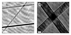
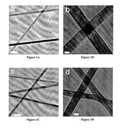
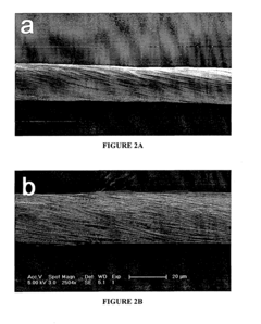
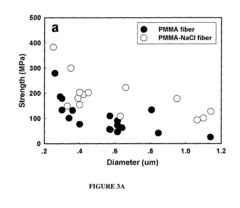
Electrospun doped nanofibers and process of preparation thereof
PatentInactiveUS20130115456A1
Innovation
- Doping polymers with an alkali salt, such as sodium chloride, during the electrospinning process to improve the mechanical properties of nanofibers, including tensile strength, stiffness, and toughness, by adjusting the molar ratio and concentration of the salt within the polymer solution.
Emulsion-based control of electrospun fiber morphology
PatentWO2005098099A1
Innovation
- Using a multiphasic composition such as a water/oil emulsion or double emulsion as a fiber-forming medium, where the first component has a lower evaporation rate and the second component has a higher evaporation rate, allowing for the control of fiber morphology by varying the ratio of components and applying a force to extrude the emulsion into fibers with specific morphologies, such as flattened and porous forms.
Material Science Advancements for Electrospun Components
Recent advancements in material science have significantly propelled the field of electrospinning toward creating next-generation optoelectronic components. The development of novel polymers with enhanced electrical conductivity, optical transparency, and mechanical flexibility has been crucial in this evolution. Particularly, the incorporation of conductive nanomaterials such as carbon nanotubes, graphene, and metallic nanoparticles into polymer matrices has created composite materials with exceptional properties suitable for optoelectronic applications.
The emergence of conjugated polymers specifically designed for electrospinning represents a breakthrough in material science. These polymers combine the processability of conventional polymers with the electronic properties of semiconductors, enabling the fabrication of electrospun fibers with intrinsic conductivity. Materials such as PEDOT:PSS, P3HT, and various polythiophene derivatives have demonstrated remarkable performance in electrospun configurations.
Hybrid organic-inorganic materials have also gained significant attention in the electrospinning community. These materials combine the flexibility and processability of organic polymers with the superior electronic properties of inorganic semiconductors. For instance, perovskite-polymer composites have shown exceptional promise for electrospun photovoltaic applications, offering high power conversion efficiencies while maintaining the mechanical advantages of fibrous structures.
Nanoscale engineering of material interfaces has proven critical for optimizing charge transport in electrospun optoelectronic components. Researchers have developed sophisticated core-shell architectures and gradient compositions that facilitate efficient charge separation and transport across material boundaries. These engineered interfaces minimize energy losses and enhance overall device performance.
The development of stimuli-responsive materials represents another frontier in electrospun optoelectronics. These smart materials can change their optical or electrical properties in response to external stimuli such as light, temperature, or electric fields. Such adaptive behavior enables the creation of dynamic optoelectronic systems with self-regulating capabilities.
Biodegradable and sustainable materials are increasingly being explored for electrospun optoelectronics, addressing environmental concerns associated with electronic waste. Cellulose derivatives, silk fibroin, and other biopolymers functionalized with conductive elements offer promising alternatives to conventional synthetic polymers, potentially enabling transient electronics that can harmlessly decompose after their functional lifetime.
Sustainability and Scalability of Electrospinning Processes
The sustainability and scalability of electrospinning processes represent critical factors in determining the commercial viability of next-generation optoelectronic components. Current electrospinning methods, while effective at laboratory scale, face significant challenges when transitioning to industrial production environments. These challenges include high energy consumption, solvent recovery issues, and material waste during processing.
Environmental considerations have become increasingly important as regulatory frameworks worldwide impose stricter requirements on manufacturing processes. Conventional electrospinning typically employs volatile organic compounds (VOCs) as solvents, which pose environmental hazards and health risks. Recent innovations have focused on developing green electrospinning approaches that utilize water-based systems or ionic liquids as environmentally benign alternatives, reducing the carbon footprint of the production process.
Energy efficiency remains a major concern in scaling electrospinning operations. The high voltage requirements (typically 10-30 kV) translate to substantial energy consumption when implemented at industrial scale. Research into low-voltage electrospinning techniques has shown promising results, with some systems operating effectively at voltages below 5 kV while maintaining fiber quality, potentially reducing energy demands by up to 70%.
Material utilization efficiency presents another challenge, as traditional single-needle electrospinning setups suffer from low throughput and inconsistent fiber deposition. Multi-needle arrays and needleless electrospinning technologies have emerged as solutions, increasing production rates by orders of magnitude. For instance, free surface electrospinning can produce fibers at rates exceeding 1 kg/hour compared to conventional methods yielding only grams per hour.
Economic viability depends on achieving consistent quality at scale. Recent advances in in-line monitoring systems using machine vision and AI-based quality control have demonstrated the ability to maintain fiber diameter consistency within ±5% during continuous production runs, addressing a key barrier to industrial adoption.
The integration of electrospinning into existing manufacturing lines represents another scalability challenge. Modular electrospinning units that can be incorporated into roll-to-roll processing systems have been developed, allowing for continuous production of functional optoelectronic components. These systems demonstrate throughput increases of up to 200% compared to batch processing methods.
Long-term sustainability will require closed-loop systems that recover and reuse solvents and minimize waste. Emerging technologies combining electrospinning with supercritical CO2 extraction have shown promise in recovering up to 95% of solvents used in the process, significantly reducing environmental impact and operational costs while maintaining the optical and electronic properties essential for next-generation devices.
Unlock deeper insights with Patsnap Eureka Quick Research — get a full tech report to explore trends and direct your research. Try now!
Generate Your Research Report Instantly with AI Agent
Supercharge your innovation with Patsnap Eureka AI Agent Platform!