

GaN HEMT Integration In 5G Base Stations
SEP 5, 20259 MIN READ
Generate Your Research Report Instantly with AI Agent
PatSnap Eureka helps you evaluate technical feasibility & market potential.
GaN HEMT Evolution and Integration Goals
Gallium Nitride High Electron Mobility Transistors (GaN HEMTs) have emerged as a revolutionary technology in the telecommunications industry, particularly for 5G base stations. The evolution of GaN technology spans over three decades, beginning with early research in the 1990s focused on understanding the fundamental properties of wide-bandgap semiconductors. By the early 2000s, researchers had developed the first practical GaN HEMT devices, demonstrating their superior power handling capabilities compared to traditional silicon-based technologies.
The technological trajectory of GaN HEMTs has been characterized by continuous improvements in material quality, device architecture, and manufacturing processes. Early challenges included high defect densities in GaN epitaxial layers and reliability issues under high-voltage operation. These obstacles have been progressively overcome through innovations in substrate materials, epitaxial growth techniques, and device passivation methods.
A significant milestone in GaN HEMT development occurred around 2010 with the commercialization of GaN-on-SiC (Silicon Carbide) technology, which offered enhanced thermal management capabilities critical for high-power RF applications. The subsequent development of GaN-on-Silicon technology represented another pivotal advancement, substantially reducing manufacturing costs while maintaining acceptable performance metrics for many applications.
The integration goals for GaN HEMTs in 5G base stations are multifaceted and ambitious. Primary objectives include achieving higher power densities exceeding 10 W/mm, improving power-added efficiency to over 70% across broad frequency bands, and enhancing linearity to meet stringent spectral emission requirements. These performance targets are essential for supporting the increased data throughput and spectral efficiency demands of 5G networks.
Another critical integration goal involves thermal management optimization, as GaN HEMTs in 5G base stations operate at significantly higher power levels than previous generation technologies. Advanced packaging solutions incorporating diamond heat spreaders and microchannel cooling systems are being developed to address these thermal challenges.
Reliability enhancement represents a paramount integration objective, with the industry targeting mean time to failure exceeding 10^7 hours at operating junction temperatures above 200°C. This requires innovations in passivation layers, gate structures, and field-plate designs to mitigate electron trapping and current collapse phenomena.
Cost reduction through improved manufacturing yields and process standardization constitutes another essential integration goal. The telecommunications industry is driving toward GaN HEMT solutions that deliver superior performance while approaching cost parity with legacy silicon LDMOS technology, particularly for mid-power applications in massive MIMO systems.
5G Market Demand for GaN HEMT Technology
The global 5G market has witnessed exponential growth since its commercial deployment in 2019, creating substantial demand for advanced semiconductor technologies like Gallium Nitride High Electron Mobility Transistors (GaN HEMTs). Market research indicates that the 5G infrastructure market is projected to reach $47.8 billion by 2027, with a compound annual growth rate of 67.1% from 2020 to 2027, driving significant demand for GaN HEMT technology.
Base station infrastructure represents the largest segment within the 5G deployment ecosystem, accounting for approximately 60% of total network investment. The technical requirements for these base stations—particularly power amplification efficiency, bandwidth capability, and thermal management—have created a distinct market pull for GaN HEMT solutions over traditional silicon-based technologies.
Telecom operators worldwide are facing increasing pressure to optimize their capital expenditure while delivering enhanced network performance. GaN HEMTs address this market need by offering superior power density (up to 5 times higher than silicon), higher efficiency (reducing operational costs by 15-20%), and broader bandwidth capabilities essential for 5G's multi-band operation. These benefits translate to smaller form factors and reduced cooling requirements, directly addressing operators' total cost of ownership concerns.
Regional market analysis reveals varying adoption rates, with North America and Asia-Pacific leading GaN HEMT implementation in 5G infrastructure. China alone plans to deploy over 600,000 5G base stations annually through 2025, creating sustained demand for GaN components. European markets show growing interest, particularly as countries accelerate their 5G deployment timelines following pandemic-related delays.
Industry surveys indicate that 78% of telecom equipment manufacturers now consider GaN technology essential for their 5G product roadmaps, compared to just 35% during the 4G era. This represents a fundamental shift in market requirements rather than merely an incremental improvement preference.
The sub-6 GHz 5G segment currently dominates the market demand for GaN HEMTs, accounting for 70% of deployments. However, the millimeter-wave segment is expected to grow at a faster rate (85% CAGR) through 2026, creating new specialized requirements for GaN technology optimization. This bifurcation in the market creates distinct product development opportunities for semiconductor manufacturers.
Supply chain analysis reveals growing concerns about GaN HEMT availability, with current production capacity meeting only 65% of projected demand through 2023. This supply-demand gap has created premium pricing opportunities for established manufacturers while simultaneously attracting new market entrants, particularly from Japan, Taiwan, and emerging European fabrication facilities.
GaN HEMT Technical Challenges in Base Stations
GaN HEMT technology faces several significant challenges when implemented in 5G base stations. The high-frequency operation required for 5G applications (particularly in mmWave bands) pushes GaN devices to their physical limits, creating thermal management issues that become increasingly critical. As power densities increase, heat dissipation becomes a major concern, with junction temperatures potentially exceeding 200°C under high-power operation, threatening device reliability and performance.
Material defects present another substantial challenge. Despite advancements in epitaxial growth techniques, GaN substrates still contain significant dislocation densities (typically 10^6-10^9 cm^-2), which can lead to premature device degradation, current collapse phenomena, and reduced mean time to failure. These defects become particularly problematic as device dimensions shrink to accommodate higher frequencies.
The integration of GaN HEMTs with silicon-based control circuitry presents significant interface challenges. The heterogeneous integration of these disparate material systems often results in thermal expansion mismatches, creating mechanical stress that can lead to delamination or cracking during thermal cycling. This integration complexity increases manufacturing costs and reduces yield rates.
Reliability concerns remain paramount for telecom infrastructure applications. GaN HEMTs must maintain stable performance over 10+ year operational lifetimes under varying environmental conditions. Current collapse and gate leakage mechanisms, particularly under high-voltage switching conditions, continue to challenge long-term device stability. Accelerated life testing protocols often fail to accurately predict field performance.
Cost factors significantly impact widespread adoption. While GaN offers superior performance, the manufacturing processes remain more expensive than silicon alternatives. The substrate costs, specialized epitaxial growth requirements, and lower yields contribute to higher component prices, making cost-benefit analysis critical for system designers.
RF linearity and efficiency tradeoffs present ongoing design challenges. As 5G systems employ complex modulation schemes with high peak-to-average power ratios, GaN amplifiers must maintain linearity while preserving efficiency. Digital predistortion techniques help mitigate nonlinearities but add system complexity and power consumption.
Packaging technology for GaN devices requires specialized approaches to manage thermal, electrical, and mechanical considerations simultaneously. Traditional packaging solutions often limit the full performance potential of GaN devices, particularly in terms of thermal resistance and parasitic inductances that become critical at mmWave frequencies.
Current GaN HEMT Implementation Strategies
01 GaN HEMT device structure and fabrication
GaN HEMT devices are fabricated with specific structural elements to optimize performance. These include the design of the gate, source, and drain regions, as well as the epitaxial layer structure. Advanced fabrication techniques are employed to create high-quality GaN layers on various substrates, with careful attention to interface quality and defect reduction. The device structure often incorporates field plates, passivation layers, and specialized buffer layers to enhance electron mobility and device reliability.- GaN HEMT device structure and fabrication: Gallium Nitride High Electron Mobility Transistors (GaN HEMTs) have specific structural designs and fabrication methods that enhance their performance. These devices typically include multiple layers such as buffer layers, channel layers, barrier layers, and specialized gate structures. Advanced fabrication techniques are employed to create these structures, including epitaxial growth methods, etching processes, and metallization techniques that optimize the electron mobility and power handling capabilities of the transistor.
- Power electronics applications of GaN HEMTs: GaN HEMTs are widely used in power electronics applications due to their high breakdown voltage, low on-resistance, and high-frequency operation capabilities. These transistors enable more efficient power conversion in applications such as power supplies, motor drives, and renewable energy systems. The unique properties of GaN allow for smaller device footprints, reduced cooling requirements, and overall system miniaturization while maintaining high power density and efficiency.
- RF and microwave applications of GaN HEMTs: GaN HEMTs excel in radio frequency (RF) and microwave applications due to their high electron mobility, high power density, and excellent high-frequency performance. These devices are used in telecommunications infrastructure, radar systems, satellite communications, and military applications. The wide bandgap properties of GaN enable operation at higher temperatures and voltages compared to conventional semiconductor materials, making them ideal for high-power RF amplifiers and transmitters.
- Reliability and thermal management of GaN HEMTs: Reliability and thermal management are critical aspects of GaN HEMT technology. Various approaches have been developed to address challenges such as current collapse, gate leakage, and thermal degradation. These include passivation techniques, field plate structures, advanced packaging solutions, and thermal management strategies. Improving the reliability of GaN HEMTs involves understanding and mitigating failure mechanisms through materials engineering and device design optimization.
- Novel GaN HEMT architectures and materials: Research in GaN HEMT technology has led to novel device architectures and material systems that further enhance performance. These innovations include vertical GaN structures, enhancement-mode designs, hybrid material systems, and integration with other semiconductor technologies. Advanced epitaxial growth techniques and substrate engineering approaches are being developed to reduce defects and improve crystal quality. These novel architectures aim to overcome the limitations of conventional GaN HEMTs and expand their application range.
02 Power electronics applications of GaN HEMTs
GaN HEMTs are increasingly utilized in power electronics applications due to their high breakdown voltage, low on-resistance, and fast switching capabilities. These devices enable more efficient power conversion systems in applications such as power supplies, motor drives, and renewable energy systems. The wide bandgap properties of GaN allow for operation at higher temperatures and voltages compared to silicon-based devices, resulting in smaller, more efficient power electronic systems with reduced cooling requirements.Expand Specific Solutions03 RF and microwave applications of GaN HEMTs
GaN HEMTs excel in radio frequency (RF) and microwave applications due to their high electron mobility, high power density, and high frequency operation capabilities. These devices are used in radar systems, wireless communication infrastructure, and satellite communications. The ability to operate at high frequencies while handling significant power levels makes GaN HEMTs ideal for amplifiers in these applications, offering improved efficiency and bandwidth compared to traditional semiconductor technologies.Expand Specific Solutions04 Reliability and thermal management of GaN HEMTs
Ensuring the reliability and effective thermal management of GaN HEMTs is crucial for their commercial success. Various techniques are employed to address challenges such as current collapse, gate leakage, and thermal degradation. These include specialized passivation techniques, buffer layer optimization, and innovative packaging solutions. Advanced thermal management strategies help dissipate heat efficiently from these high-power-density devices, extending their operational lifetime and maintaining performance under demanding conditions.Expand Specific Solutions05 Novel materials and structures for enhanced GaN HEMT performance
Research continues to develop novel materials and structures to enhance GaN HEMT performance. These innovations include alternative substrates, advanced barrier layers, and novel gate architectures. Integration of complementary materials such as AlGaN, InAlN, or SiC helps optimize device characteristics. Emerging approaches like polarization engineering, heterostructure designs, and nanostructured elements are being explored to push the boundaries of GaN HEMT capabilities, enabling higher frequencies, greater power handling, and improved efficiency.Expand Specific Solutions
Leading GaN HEMT Manufacturers and Suppliers
The GaN HEMT integration in 5G base stations market is currently in a growth phase, with an expanding market size driven by increasing 5G infrastructure deployment globally. The technology has reached moderate maturity, with key players advancing commercial solutions while continuing R&D efforts. Wolfspeed leads in GaN substrate development, while Huawei and ZTE are integrating GaN HEMT technology into commercial 5G base stations. Research institutions like UESTC and SINANO collaborate with industry partners to overcome technical challenges. Companies like Innoscience and Jiangxi Zhaochi are emerging as specialized GaN device manufacturers. UMC and SK hynix provide semiconductor manufacturing support, while system integrators like Fujitsu and NTT implement the technology in network infrastructure, creating a competitive ecosystem balancing innovation and commercialization.
Fujitsu Ltd.
Technical Solution: Fujitsu has developed a comprehensive GaN HEMT integration solution for 5G base stations based on their long-standing expertise in compound semiconductor technologies. Their approach utilizes GaN-on-SiC technology with proprietary epitaxial growth techniques that minimize crystal defects and optimize 2DEG formation. Fujitsu's GaN HEMTs feature a T-shaped gate structure with gate lengths below 0.15μm, enabling operation at frequencies up to 40GHz with minimal gate resistance. For 5G applications, they've implemented a distributed power amplifier architecture that maintains flat gain across wide bandwidths, critical for supporting multiple 5G frequency bands with a single hardware platform. Their solution incorporates advanced thermal management techniques including diamond heat spreaders that reduce junction temperatures by up to 30°C compared to conventional approaches[9]. Fujitsu has developed specialized GaN MMIC designs that integrate driver stages, power stages, and matching networks on a single chip, reducing parasitic effects and improving overall efficiency. Their latest generation devices achieve power-added efficiencies exceeding 55% at 28GHz while maintaining linearity metrics suitable for complex modulation schemes used in 5G systems[10]. Fujitsu's GaN technology also features built-in monitoring capabilities that provide real-time data on device performance and reliability parameters.
Strengths: Extensive experience in compound semiconductor manufacturing ensures high yield and reliability; advanced thermal solutions enable sustained high-power operation; integrated approach reduces system complexity and improves performance. Weaknesses: Higher cost structure compared to some competitors; limited market share in base station equipment outside Japan; requires specialized design expertise to fully leverage technology capabilities.
Wolfspeed, Inc.
Technical Solution: Wolfspeed has pioneered GaN HEMT technology for 5G base stations with their advanced GaN-on-SiC (Silicon Carbide) solutions. Their technology delivers high-frequency performance up to 100GHz with power densities exceeding 5W/mm[1]. Wolfspeed's GaN HEMTs feature proprietary passivation techniques that significantly reduce current collapse and enhance reliability under high-voltage operation. Their latest generation devices incorporate field plates and optimized gate structures to achieve breakdown voltages above 200V while maintaining high transconductance. For 5G applications, Wolfspeed has developed GaN HEMT MMICs (Monolithic Microwave Integrated Circuits) that integrate multiple functions including power amplification, switching, and filtering on a single chip, reducing system complexity and improving thermal management. Their devices demonstrate power-added efficiencies exceeding 60% at 28GHz[2], making them ideal for 5G millimeter-wave deployments.
Strengths: Superior thermal conductivity of SiC substrate enables higher power handling; industry-leading reliability with MTTF >1 million hours at 200°C; excellent linearity for complex modulation schemes. Weaknesses: Higher manufacturing costs compared to silicon-based solutions; requires specialized packaging to maximize thermal performance; more complex biasing requirements than traditional technologies.
Key GaN HEMT Patents and Technical Innovations
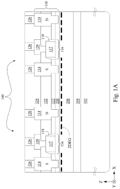
Gallium nitride high electron mobility transistor
PatentPendingUS20230395694A1
Innovation
- The solution involves forming a second AlGaN layer with a different composition over the AlGaN-GaN heterojunction, using sidewall spacers and selective epitaxy to decouple on-resistance from the threshold voltage, achieved by increasing the aluminum concentration in the AlGaN layer and adjusting its thickness, thereby enhancing spontaneous and piezoelectric polarization effects.
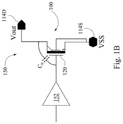
Pulse Width Control Apparatus and Method
PatentActiveUS20230396238A1
Innovation
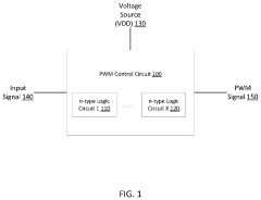
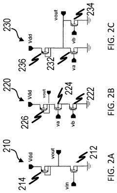
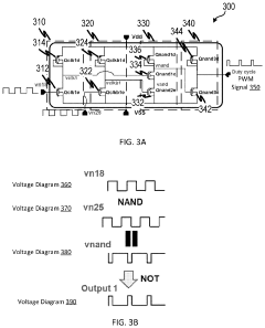
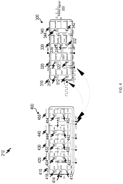
- Implementing logic circuitry using only n-type HEMTs to generate PWM signals with minimal to no power loss, utilizing a combination of enhancement mode (E-HEMTs) and depletion mode (D-HEMTs) in series to control duty cycles without the need for additional components like sawtooth generators, level shifters, or comparators.
Thermal Management Solutions for GaN HEMT
Thermal management represents a critical challenge in GaN HEMT integration for 5G base stations due to the high power density and operating temperatures of these devices. Current thermal management solutions employ multi-layered approaches to effectively dissipate heat and maintain optimal device performance.
Advanced packaging technologies play a crucial role in thermal management, with direct copper bonding (DCB) and direct bonded copper (DBC) substrates offering superior thermal conductivity compared to traditional materials. These substrates typically achieve thermal conductivities of 24-170 W/m·K, significantly enhancing heat dissipation from GaN devices to heat sinks.
Diamond-based heat spreaders represent the cutting edge of thermal management solutions, with thermal conductivity exceeding 1500 W/m·K. Though expensive, these materials are increasingly deployed in high-power density applications where thermal performance is paramount. Companies like Element Six and Sumitomo Electric have commercialized synthetic diamond heat spreaders specifically designed for GaN HEMT applications.
Liquid cooling systems have gained traction in 5G base station designs, offering thermal resistance values as low as 0.1°C/W compared to 0.3-0.5°C/W for advanced air cooling. These systems utilize microchannels etched directly into heat sinks or cold plates, with coolants circulating to extract heat more efficiently than conventional air cooling methods.
Phase change materials (PCMs) provide another innovative approach, absorbing heat during power spikes through latent heat of fusion. PCMs with melting points between 80-120°C are particularly suitable for GaN HEMT applications, offering thermal buffering during transient operations.
Computational fluid dynamics (CFD) modeling has become essential in thermal solution design, enabling engineers to predict hotspots and optimize thermal interfaces before physical prototyping. Advanced simulation tools from companies like ANSYS and COMSOL now incorporate GaN-specific material properties and operating parameters.
Recent developments include the integration of AI-driven thermal management systems that dynamically adjust cooling parameters based on real-time temperature monitoring. These systems can reduce cooling power consumption by 15-30% while maintaining optimal device temperatures, addressing both thermal and energy efficiency concerns in 5G infrastructure deployment.
Industry standards for thermal management in GaN applications continue to evolve, with JEDEC and IEEE developing specialized guidelines for wide bandgap semiconductor thermal characterization and management in telecommunications infrastructure.
Reliability Testing Standards for GaN RF Components
Reliability testing standards for GaN RF components in 5G base stations have evolved significantly to address the unique challenges posed by gallium nitride high-electron-mobility transistors (GaN HEMTs). These standards encompass a comprehensive framework designed to ensure the robustness and longevity of GaN components under the demanding operational conditions of 5G infrastructure.
The Joint Electron Device Engineering Council (JEDEC) has established specific qualification standards for GaN devices, including JEP180 and JESD22, which outline rigorous testing protocols for high-frequency applications. These standards mandate accelerated life testing at elevated temperatures (typically 150-175°C) for periods ranging from 1,000 to 5,000 hours to simulate long-term operational stress.
RF-specific reliability tests for GaN components include load-pull characterization under various impedance conditions, which is critical for evaluating performance in 5G base station environments where impedance matching significantly impacts efficiency. The IEC 62108 standard provides guidelines for thermal cycling tests (-40°C to +125°C), essential for evaluating the thermal resilience of GaN devices in outdoor base station deployments.
Power cycling tests represent another crucial reliability metric, with standards requiring components to withstand 10,000 to 100,000 cycles without significant degradation in performance parameters. This is particularly relevant for 5G applications where dynamic power management leads to frequent operational state changes.
The telecommunications industry has developed specialized standards through organizations like ETSI and 3GPP that address the unique reliability requirements of 5G RF front-end modules. These standards specify minimum mean time between failures (MTBF) of 100,000 hours for critical components and define acceptable degradation thresholds for key parameters such as output power, gain, and efficiency over time.
Environmental testing standards have been enhanced for GaN RF components, incorporating humidity resistance tests (85% RH at 85°C for 1,000 hours) and salt fog exposure tests to simulate coastal deployment conditions. These tests are particularly important as 5G networks expand into diverse geographical locations with varying environmental challenges.
Radiation hardness testing has emerged as an important consideration, with standards specifying tolerance levels for total ionizing dose (TID) and single event effects (SEE), ensuring GaN components can operate reliably in environments with elevated electromagnetic radiation levels common in dense urban 5G deployments.
Unlock deeper insights with PatSnap Eureka Quick Research — get a full tech report to explore trends and direct your research. Try now!
Generate Your Research Report Instantly with AI Agent
Supercharge your innovation with PatSnap Eureka AI Agent Platform!