

How Do GaN HEMTs Support Fast Charging Infrastructure?
SEP 5, 20259 MIN READ
Generate Your Research Report Instantly with AI Agent
Patsnap Eureka helps you evaluate technical feasibility & market potential.
GaN HEMT Technology Evolution and Objectives
Gallium Nitride High Electron Mobility Transistors (GaN HEMTs) have emerged as revolutionary semiconductor devices that are transforming power electronics. The evolution of this technology began in the early 1990s when researchers first demonstrated the unique properties of GaN as a wide bandgap semiconductor material. By the early 2000s, the first commercial GaN HEMTs were introduced, primarily for RF applications in telecommunications and defense sectors.
The technological trajectory of GaN HEMTs has been marked by significant milestones in material quality improvement, device architecture optimization, and manufacturing scalability. Initially limited by substrate quality and defect density issues, the technology has progressively overcome these challenges through innovations in epitaxial growth techniques and device fabrication processes. The introduction of enhancement-mode GaN HEMTs around 2010 represented a pivotal advancement, enabling normally-off operation critical for power switching applications.
Fast charging infrastructure represents one of the most promising application domains for GaN HEMTs. The fundamental technical advantages driving this synergy include GaN's superior electron mobility, higher breakdown voltage, and significantly reduced on-resistance compared to silicon-based alternatives. These properties enable power conversion systems with unprecedented efficiency, operating frequencies, and power density – all critical parameters for next-generation charging solutions.
The current technological objectives for GaN HEMTs in fast charging applications focus on several key areas. First, increasing the voltage handling capability beyond 650V toward 1200V and even 1700V ratings to accommodate higher power charging stations. Second, enhancing thermal management solutions to handle the concentrated heat generation in compact charging systems. Third, improving reliability and robustness under the demanding operational conditions typical of public charging infrastructure.
Industry roadmaps project continued performance improvements, with particular emphasis on reducing dynamic RDS(on) effects, minimizing parasitic inductances, and developing advanced packaging solutions that maximize the inherent benefits of GaN technology. The integration of GaN devices with sophisticated control algorithms and protection mechanisms represents another critical development path, enabling intelligent power management systems that can adapt to varying load conditions and grid requirements.
The ultimate technological goal is to establish GaN HEMTs as the dominant semiconductor technology for fast charging infrastructure, supporting charging powers exceeding 350kW with system efficiencies above 98%, while simultaneously reducing form factors by 70-80% compared to silicon-based solutions. This evolution aligns perfectly with the broader electrification trends in transportation and the growing demand for rapid, efficient energy transfer systems.
Fast Charging Market Demand Analysis
The global fast charging market is experiencing unprecedented growth, driven by the rapid adoption of electric vehicles (EVs) and portable electronic devices. Market research indicates that the fast charging infrastructure market is projected to reach $25.5 billion by 2027, with a compound annual growth rate of approximately 26.8% from 2020. This explosive growth is primarily fueled by government initiatives promoting electric mobility, increasing consumer demand for reduced charging times, and technological advancements in power electronics.
Consumer behavior analysis reveals a significant shift in charging preferences, with EV owners increasingly prioritizing charging speed as a critical factor in purchase decisions. A recent survey conducted across major EV markets showed that 78% of potential EV buyers consider charging time a decisive factor, with 65% expressing willingness to pay premium prices for vehicles supporting ultra-fast charging capabilities. This consumer sentiment has created substantial market pull for advanced charging solutions.
The commercial sector represents another significant demand driver, with fleet operators requiring minimal vehicle downtime to maintain operational efficiency. Public transportation authorities, logistics companies, and ride-sharing services are investing heavily in fast charging infrastructure to support their electrification goals. These commercial applications demand charging systems capable of delivering high power levels consistently while maintaining reliability and safety.
Regional analysis shows varying market maturity levels, with Europe leading in fast charging infrastructure deployment, followed by China and North America. European markets benefit from stringent emission regulations and substantial government incentives, while China's growth is driven by national policies promoting EV adoption. North American markets are experiencing accelerated growth as automotive manufacturers expand their EV offerings and charging networks.
The demand for higher power density and efficiency in fast charging systems directly correlates with the need for advanced semiconductor technologies. Traditional silicon-based power devices are approaching their theoretical limits in handling the high voltage and current requirements of modern fast chargers. This technological bottleneck has created market demand for wide-bandgap semiconductors, particularly Gallium Nitride (GaN) High Electron Mobility Transistors (HEMTs).
Industry forecasts indicate that the market share of GaN-based fast charging solutions will grow from 8% in 2021 to approximately 32% by 2026, reflecting the technology's superior performance characteristics. The ability of GaN HEMTs to operate at higher frequencies enables smaller form factors and reduced cooling requirements, addressing key consumer demands for portable and efficient charging solutions.
GaN HEMT Current Status and Technical Challenges
Gallium Nitride High Electron Mobility Transistors (GaN HEMTs) have emerged as a revolutionary technology in power electronics, particularly for fast charging infrastructure. Currently, GaN HEMTs are transitioning from research laboratories to commercial applications, with significant market penetration in consumer electronics and growing adoption in electric vehicle charging systems. The global market for GaN power devices reached approximately $223 million in 2022 and is projected to exceed $2 billion by 2027, demonstrating the technology's commercial viability and increasing industry acceptance.
Despite this progress, GaN HEMT technology faces several critical technical challenges that limit its broader implementation in fast charging infrastructure. Thermal management remains a primary concern, as GaN devices generate significant heat during high-power operation. Current thermal dissipation solutions are often inadequate for the power densities achieved in advanced charging applications, leading to reliability issues and performance degradation under sustained operation.
Reliability and robustness present another major challenge. GaN HEMTs exhibit various degradation mechanisms including current collapse, dynamic on-resistance increase, and gate leakage that can compromise device performance over time. These issues become particularly pronounced in fast charging applications where devices must withstand high voltages, currents, and switching frequencies simultaneously.
Manufacturing scalability continues to constrain widespread adoption. While 6-inch GaN-on-Si wafers are now standard, the industry is struggling with the transition to 8-inch wafers needed for cost-effective mass production. Defect densities, particularly in the epitaxial layers, remain higher than desired, affecting yield rates and increasing production costs compared to mature silicon technologies.
Integration challenges persist at the system level. GaN HEMTs require specialized gate drivers and protection circuits that differ significantly from silicon-based solutions. The ultra-fast switching speeds (>200 V/ns) create electromagnetic interference (EMI) issues that demand careful circuit layout and shielding techniques not commonly employed in traditional power electronics.
Standardization and qualification frameworks specific to GaN technology are still evolving. The absence of universally accepted reliability testing protocols and application-specific standards creates uncertainty for system designers and slows adoption in mission-critical charging infrastructure.
Geographically, GaN HEMT technology development shows distinct patterns. The United States and Japan lead in fundamental research and intellectual property, while Taiwan and China dominate in manufacturing capacity. Europe maintains strength in automotive-grade qualification and system-level integration, creating a globally distributed technology ecosystem that complicates supply chain management for fast charging infrastructure developers.
Current GaN-based Fast Charging Solutions
01 GaN HEMT device structures for fast charging applications
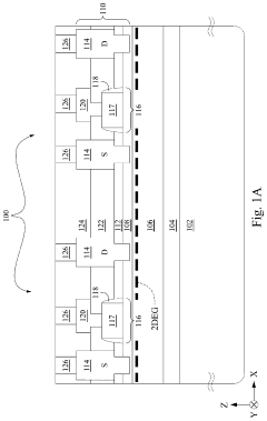
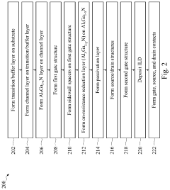
Specific structural designs of GaN HEMTs that enhance their performance in fast charging applications. These designs include optimized gate configurations, channel structures, and substrate materials that improve electron mobility and reduce resistance. The enhanced electron transport properties allow for higher power density and faster charging capabilities while maintaining thermal stability during high-power operation.- GaN HEMT device structure optimization for fast charging: Optimizing the structure of GaN HEMT devices can significantly improve their performance in fast charging applications. This includes modifications to the gate design, channel structure, and substrate materials. Enhanced electron mobility in the two-dimensional electron gas (2DEG) layer and reduced on-resistance contribute to higher efficiency and faster charging capabilities. These structural optimizations allow for higher power density and improved thermal management during rapid charging cycles.
- Power conversion efficiency improvements in GaN-based charging systems: GaN HEMTs enable significant improvements in power conversion efficiency for fast charging applications. Their ability to operate at higher frequencies with lower switching losses compared to silicon-based devices results in more compact and efficient power adapters. Advanced circuit topologies leveraging GaN HEMTs' unique properties can achieve efficiency rates exceeding 95% while supporting higher power densities. These improvements directly translate to faster charging speeds and reduced energy waste in charging infrastructure.
- Thermal management solutions for GaN HEMT fast chargers: Effective thermal management is crucial for GaN HEMT-based fast charging systems to maintain reliability and performance. Various approaches include advanced packaging techniques, integrated heat spreaders, and novel cooling solutions. Improved thermal interfaces between the GaN device and heat dissipation components help manage the high power density during fast charging operations. These thermal solutions enable sustained high-power operation without degradation, allowing for consistent fast charging performance over extended periods.
- Protection and reliability enhancements for GaN fast charging: GaN HEMT fast charging systems incorporate specialized protection circuits and reliability enhancements to ensure safe operation under high-power conditions. These include overvoltage protection, current limiting features, and temperature monitoring systems specifically designed for the unique characteristics of GaN devices. Advanced gate drivers with precise timing control prevent damaging voltage spikes during high-frequency switching. These protection mechanisms enable safe deployment of GaN technology in consumer fast charging products while maintaining long-term reliability.
- Integration of GaN HEMTs in compact fast charging systems: The superior properties of GaN HEMTs enable the development of extremely compact fast charging systems. Integration techniques include embedding GaN devices in advanced packaging solutions, utilizing multi-chip modules, and implementing novel circuit layouts to minimize parasitic effects. The high power density capabilities allow for miniaturization of charging adapters while maintaining or improving charging speeds. These integration approaches result in portable, high-power fast chargers that are significantly smaller than traditional silicon-based solutions.
02 Power conversion efficiency improvements in GaN HEMT chargers
Techniques to improve power conversion efficiency in GaN HEMT-based fast charging systems. These include advanced switching topologies, gate driving methods, and circuit designs that minimize switching and conduction losses. The high electron mobility and breakdown voltage of GaN HEMTs enable higher frequency operation with reduced switching losses, resulting in more efficient and compact fast charging solutions.Expand Specific Solutions03 Thermal management solutions for GaN HEMT fast chargers
Thermal management approaches specifically designed for GaN HEMT-based fast charging systems. These solutions address the heat dissipation challenges associated with high-power density operation, including advanced packaging techniques, heat spreading materials, and thermal interface optimizations. Effective thermal management ensures reliable operation and longer device lifetime while maintaining the high performance needed for fast charging applications.Expand Specific Solutions04 Integration of GaN HEMTs in fast charging systems
System-level integration approaches for incorporating GaN HEMTs into fast charging solutions. These include power delivery architectures, control algorithms, and protection mechanisms that leverage the high-speed switching capabilities of GaN devices. The integration strategies enable compact, efficient, and reliable fast charging systems for various applications including mobile devices, electric vehicles, and industrial equipment.Expand Specific Solutions05 Manufacturing and reliability enhancements for GaN HEMT chargers
Manufacturing processes and reliability improvement techniques for GaN HEMT-based fast charging solutions. These include passivation methods, edge termination designs, and quality control processes that enhance device robustness and consistency. The manufacturing innovations address common reliability concerns such as current collapse, dynamic on-resistance, and gate leakage, ensuring stable performance over the lifetime of fast charging products.Expand Specific Solutions
Leading GaN HEMT Manufacturers and Competitors
GaN HEMT fast charging infrastructure is in a growth phase, with the market expanding rapidly due to increasing demand for efficient power conversion in electric vehicles and consumer electronics. The technology has reached moderate maturity, with key players driving innovation across different segments. Companies like Texas Instruments, Qualcomm, and Huawei are leading commercial applications, while Power Integrations and MACOM focus on specialized power management solutions. Research institutions such as Xidian University and UESTC collaborate with industry leaders like Fujitsu and Nichia to advance fundamental GaN technology. The competitive landscape shows a balance between established semiconductor manufacturers and emerging GaN specialists, with increasing integration between device manufacturers and system solution providers.
Texas Instruments Incorporated
Technical Solution: Texas Instruments has developed comprehensive GaN HEMT solutions specifically engineered for fast charging infrastructure. Their LMG341x family of GaN power stages integrates drivers, protection features, and GaN FETs in a single package, enabling power densities up to 4x higher than silicon alternatives. TI's approach focuses on system-level optimization, with their GaN devices achieving switching frequencies of 1-2MHz while maintaining efficiency above 95%. Their technology incorporates advanced thermal design to manage the unique challenges of GaN operation, including specialized packaging that minimizes parasitic inductance. TI has also developed dedicated controller ICs that maximize the performance benefits of GaN HEMTs in fast charging applications. Their solutions support USB Power Delivery and other fast charging protocols, with power capabilities ranging from 65W to 240W for various charging scenarios.
Strengths: Extensive power management ecosystem supporting GaN implementation; strong integration capabilities combining drivers and protection with GaN FETs; robust supply chain. Weaknesses: Less vertical integration in end-product manufacturing compared to some competitors; higher system complexity requiring more design expertise.
Huawei Technologies Co., Ltd.
Technical Solution: Huawei has developed advanced GaN HEMT-based fast charging solutions that leverage their proprietary SuperCharge technology. Their approach integrates high-frequency GaN power devices with sophisticated power conversion architectures to achieve charging speeds up to 66W and beyond. Huawei's GaN HEMTs feature optimized gate structures that minimize on-resistance while maintaining high breakdown voltage capabilities, enabling efficient operation at frequencies exceeding 1MHz. This allows for significantly smaller passive components in their charger designs. Their technology implements advanced thermal management systems and multi-level protection mechanisms to ensure safety during high-power operation. Huawei has also pioneered intelligent charging protocols that dynamically adjust power delivery based on device temperature and battery state, maximizing charging speed while preserving battery longevity.
Strengths: Vertical integration allowing optimization across hardware and software; extensive deployment experience in consumer electronics; proprietary SuperCharge protocols. Weaknesses: Potential geopolitical challenges affecting global market access; higher cost structure compared to silicon-based alternatives.
Key GaN HEMT Patents and Technical Innovations
Gallium nitride high electron mobility transistor
PatentPendingUS20230395694A1
Innovation
- The solution involves forming a second AlGaN layer with a different composition over the AlGaN-GaN heterojunction, using sidewall spacers and selective epitaxy to decouple on-resistance from the threshold voltage, achieved by increasing the aluminum concentration in the AlGaN layer and adjusting its thickness, thereby enhancing spontaneous and piezoelectric polarization effects.
Transistor with source field plates and non-overlapping gate runner layers
PatentActiveUS20210143258A1
Innovation
- The design includes a field plate extending from the source runner layer or source contact layer, positioned coplanar with the gate runner layer, allowing it to overlap vertically with the metal gate layer, reducing parasitic capacitance and resistance without additional routings, thus enhancing size efficiency.
Thermal Management Strategies for GaN HEMTs
Thermal management represents a critical challenge in the deployment of Gallium Nitride High Electron Mobility Transistors (GaN HEMTs) for fast charging infrastructure. Despite their superior efficiency compared to silicon-based alternatives, GaN HEMTs generate significant heat during high-power operation, which must be effectively dissipated to maintain reliability and performance.
The primary thermal management approaches for GaN HEMTs in charging applications include both passive and active cooling strategies. Passive techniques involve optimized package designs with enhanced thermal interface materials (TIMs) that facilitate heat transfer from the die to the heat sink. Advanced ceramic substrates with aluminum nitride (AlN) or silicon carbide (SiC) offer superior thermal conductivity compared to traditional FR4 materials, enabling more efficient heat dissipation pathways.
Active cooling solutions incorporate forced-air or liquid cooling systems that significantly enhance heat removal capabilities. In high-power fast charging stations exceeding 350kW, liquid cooling has become increasingly prevalent, allowing for more compact designs while maintaining safe operating temperatures. These systems typically utilize water-glycol mixtures circulated through cold plates attached directly to power modules containing GaN devices.
Thermal simulation and modeling play an essential role in optimizing these management strategies. Computational fluid dynamics (CFD) and finite element analysis (FEA) enable engineers to predict hotspots and thermal gradients before physical prototyping, reducing development cycles and improving reliability. Advanced thermal models now incorporate transient thermal behaviors that are particularly relevant for the dynamic load profiles characteristic of fast charging applications.
Innovative approaches emerging in the field include phase-change materials (PCMs) that absorb heat during peak operation and release it during idle periods, helping to smooth thermal cycles. Additionally, direct substrate cooling techniques that bring coolant channels closer to the heat source are showing promise for ultra-high-power density applications.
The industry has also developed specialized thermal management integrated circuits (TMICs) that work alongside GaN HEMTs to provide real-time temperature monitoring and dynamic power adjustment. These systems can modulate charging rates based on thermal conditions, ensuring optimal performance while preventing thermal runaway scenarios that could compromise safety or device longevity.
As charging power levels continue to increase to enable faster charging times, thermal management will remain a critical differentiator in system design. The companies that master these thermal challenges will likely gain significant competitive advantages in the fast-evolving charging infrastructure market.
Cost-Performance Analysis of GaN vs Silicon Technologies
When evaluating GaN HEMTs for fast charging infrastructure, a comprehensive cost-performance analysis compared to traditional silicon technologies reveals significant economic considerations that influence adoption decisions.
GaN HEMTs command a price premium of approximately 1.5-3x over silicon alternatives in current markets. This higher initial component cost has been a primary barrier to widespread adoption, particularly in cost-sensitive consumer applications. However, this differential is steadily narrowing as manufacturing volumes increase and production processes mature, with industry projections suggesting potential cost parity with silicon MOSFETs within 5-7 years for certain applications.
The performance advantages of GaN translate into substantial system-level cost benefits that often outweigh the higher component costs. Fast charging systems utilizing GaN can achieve 30-40% higher power density, enabling smaller form factors that reduce material costs for casings, heat sinks, and other passive components. The higher switching frequencies (typically 3-5x higher than silicon) allow for smaller magnetic components and capacitors, which can reduce overall bill of materials costs by 15-25% in optimized designs.
Energy efficiency improvements of 2-3% in GaN-based charging systems yield significant operational cost savings over product lifetimes. For commercial fast charging stations, this efficiency advantage can translate to thousands of dollars in electricity cost savings per unit annually, particularly in high-utilization scenarios such as public charging infrastructure.
Reliability metrics indicate that GaN HEMTs maintain performance characteristics over longer operational periods in high-temperature environments common in charging applications. This durability reduces maintenance and replacement costs, with mean time between failures (MTBF) rates showing 1.5-2x improvements over silicon alternatives in accelerated life testing under thermal stress conditions.
Total cost of ownership (TCO) analyses demonstrate that despite higher initial investment, GaN-based charging infrastructure typically reaches cost break-even within 12-24 months of deployment compared to silicon alternatives. This ROI timeline continues to improve as GaN manufacturing scales and component costs decrease, making the technology increasingly attractive for both consumer and commercial charging applications.
Market forecasts indicate that as economies of scale improve and manufacturing processes mature, the cost differential between GaN and silicon will continue to narrow, potentially reaching near-parity for many applications by 2026-2028, which will further accelerate adoption across the fast charging ecosystem.
Unlock deeper insights with Patsnap Eureka Quick Research — get a full tech report to explore trends and direct your research. Try now!
Generate Your Research Report Instantly with AI Agent
Supercharge your innovation with Patsnap Eureka AI Agent Platform!