

GaN HEMT Modeling For Accurate Circuit Simulation
SEP 8, 20259 MIN READ
Generate Your Research Report Instantly with AI Agent
PatSnap Eureka helps you evaluate technical feasibility & market potential.
GaN HEMT Technology Evolution and Objectives
Gallium Nitride High Electron Mobility Transistors (GaN HEMTs) have emerged as revolutionary semiconductor devices over the past three decades, transforming power electronics, RF communications, and high-frequency applications. The evolution of GaN HEMT technology began in the early 1990s with rudimentary structures, progressing through significant milestones that have continuously enhanced performance parameters including power density, efficiency, and reliability.
The fundamental advantage of GaN HEMTs lies in their wide bandgap properties (3.4 eV compared to silicon's 1.1 eV), enabling higher breakdown voltages, reduced on-resistance, and superior thermal conductivity. These inherent material characteristics have positioned GaN as the technology of choice for next-generation power and RF applications where traditional silicon-based solutions reach their physical limitations.
Early development phases focused primarily on establishing basic fabrication techniques and understanding the unique properties of the two-dimensional electron gas (2DEG) formed at the AlGaN/GaN heterojunction. This 2DEG creates a high-mobility channel without intentional doping, a distinctive feature that differentiates HEMTs from conventional transistor structures.
The technology evolution trajectory has been marked by several critical advancements: the introduction of field plates to manage peak electric fields, the development of advanced epitaxial growth techniques for reduced defect densities, and the implementation of surface passivation technologies to mitigate current collapse phenomena. Each evolutionary step has addressed specific performance limitations, gradually expanding the application scope of GaN HEMTs.
Current technological objectives center on developing accurate and computationally efficient models that can precisely predict GaN HEMT behavior across diverse operating conditions. The complexity of modeling these devices stems from their unique physical phenomena, including self-heating effects, trapping mechanisms, and nonlinear capacitances that significantly impact circuit performance.
The primary goal of GaN HEMT modeling for circuit simulation is to create physics-based models that maintain accuracy while remaining computationally viable for large-scale circuit designs. These models must capture both DC and RF characteristics, transient responses, and long-term reliability factors to enable designers to fully leverage GaN's capabilities.
Looking forward, the technology roadmap aims to address several key objectives: enhancing model scalability across device geometries, improving prediction accuracy under extreme operating conditions, incorporating degradation mechanisms for lifetime prediction, and developing parameter extraction methodologies that reduce characterization complexity. The ultimate aim is to establish standardized modeling frameworks that can accelerate GaN adoption across broader application domains.
Market Analysis for GaN HEMT Applications
The Gallium Nitride (GaN) High Electron Mobility Transistor (HEMT) market has experienced significant growth in recent years, driven by the superior performance characteristics of these devices compared to traditional silicon-based technologies. The global GaN power device market reached approximately $1.4 billion in 2022 and is projected to grow at a compound annual growth rate (CAGR) of 25% through 2028, with GaN HEMTs representing a substantial portion of this market.
The telecommunications sector remains the largest consumer of GaN HEMT technology, particularly in 5G infrastructure deployment where high-frequency operation and power efficiency are critical. Base station manufacturers have increasingly adopted GaN HEMTs for radio frequency (RF) power amplifiers, with the market share of GaN in this segment growing from 30% in 2019 to over 45% in 2023.
Defense and aerospace applications constitute the second-largest market segment, valued at approximately $380 million in 2022. Radar systems, electronic warfare equipment, and satellite communications heavily rely on GaN HEMT technology for high-power RF applications. Military investments in next-generation radar systems are expected to drive continued growth in this sector.
Consumer electronics represents an emerging market with substantial growth potential. The adoption of GaN technology in fast chargers for smartphones, laptops, and other portable devices has accelerated, with over 120 million GaN-based chargers shipped in 2022. This segment is projected to grow at 35% annually as manufacturers increasingly transition from silicon-based solutions.
The automotive sector presents perhaps the most promising long-term growth opportunity. Electric vehicle (EV) manufacturers are evaluating GaN HEMTs for onboard chargers, DC-DC converters, and traction inverters. The potential market size for GaN in automotive applications could reach $2 billion by 2030, though widespread adoption faces challenges related to reliability qualification and cost considerations.
Regionally, Asia-Pacific dominates GaN HEMT manufacturing and consumption, accounting for 58% of the global market. North America follows at 25%, with Europe representing 15%. China has made significant investments in domestic GaN production capabilities, aiming to reduce dependency on foreign technology in strategic sectors.
The accurate modeling of GaN HEMTs for circuit simulation has become increasingly important as applications expand beyond specialized RF markets into mainstream power electronics. Industry surveys indicate that 72% of design engineers cite simulation accuracy as a critical factor in their decision to adopt GaN technology, highlighting the commercial importance of advanced modeling techniques.
Current Modeling Challenges and Limitations
Despite significant advancements in GaN HEMT technology, accurate modeling for circuit simulation faces several persistent challenges. The complex physical mechanisms in GaN devices create difficulties in developing comprehensive models that capture all relevant behaviors. Current models struggle to simultaneously account for trapping effects, thermal dependencies, and frequency dispersion phenomena that are characteristic of GaN HEMTs.
Trapping effects remain particularly problematic, as they cause dynamic changes in device characteristics that are difficult to predict. Surface and buffer traps lead to current collapse and knee voltage walkout, significantly impacting RF performance. Existing models often fail to accurately represent these effects across different operating conditions, leading to discrepancies between simulated and measured results in high-frequency applications.
Thermal modeling presents another significant limitation. GaN HEMTs operate at high power densities, causing substantial self-heating that affects device performance. Current thermal models typically use simplified approaches that do not adequately capture the complex three-dimensional heat flow within these devices. This results in inaccurate predictions of temperature distribution and its impact on electrical parameters, particularly during pulsed operation or under varying duty cycles.
Nonlinear behavior modeling at high frequencies represents a critical challenge. GaN HEMTs exhibit strong nonlinearities that affect their performance in power amplifier applications. Current models often fail to accurately predict intermodulation distortion, harmonic generation, and memory effects that occur under large-signal conditions. This limitation hampers the design optimization of high-efficiency power amplifiers and other RF circuits.
Parameter extraction methodologies for GaN HEMT models remain inconsistent across the industry. The extraction process is often time-consuming and requires specialized equipment and expertise. Different extraction approaches can yield varying model parameters for the same device, leading to inconsistent simulation results. This lack of standardization complicates model sharing and validation across different design teams and tools.
Scalability issues further limit current modeling approaches. Models developed for one device size or technology variant often cannot be reliably scaled to different geometries or process variations. This forces designers to develop new models for each device variant, increasing development time and cost. The inability to create truly scalable models hampers rapid design iteration and technology optimization.
Integration with commercial circuit simulators presents additional challenges. Many advanced GaN HEMT models require custom implementation in simulation environments, limiting their accessibility and usability. Compatibility issues between model formulations and simulator capabilities can lead to convergence problems or excessive simulation times, particularly for complex circuits operating under transient conditions.
State-of-the-Art GaN HEMT Modeling Approaches
01 GaN HEMT device structure optimization for accuracy
Optimizing the device structure of GaN HEMTs is crucial for improving accuracy. This includes engineering the gate structure, channel design, and substrate selection. Advanced gate designs with reduced gate length and optimized gate-to-channel distance can minimize parasitic capacitances and improve frequency response. Channel engineering techniques such as incorporating AlGaN/GaN heterojunctions with precise composition control enhance electron mobility and confinement, leading to more accurate and predictable device performance.- GaN HEMT device structure optimization for accuracy: Optimizing the structure of GaN HEMT devices can significantly improve their accuracy and performance. This includes modifications to the gate design, channel structure, and substrate materials. Advanced epitaxial layer structures and precise control of the two-dimensional electron gas (2DEG) formation contribute to enhanced device accuracy. Structural improvements can reduce parasitic effects and improve linearity, resulting in more accurate signal processing and amplification.
- Measurement and characterization techniques for GaN HEMT accuracy: Specialized measurement and characterization techniques are essential for evaluating and improving the accuracy of GaN HEMT devices. These include advanced testing methodologies for parameters such as transconductance, threshold voltage, and frequency response. High-precision characterization tools enable more accurate modeling of device behavior under various operating conditions, leading to better prediction of performance and reliability in practical applications.
- Thermal management solutions for improved GaN HEMT accuracy: Thermal management is crucial for maintaining the accuracy of GaN HEMT devices, especially under high-power operation. Various cooling strategies and heat dissipation techniques can be implemented to reduce thermal-induced performance variations. Improved thermal stability leads to more consistent device characteristics, reducing drift in critical parameters and enhancing overall measurement accuracy in applications requiring precise signal processing.
- Advanced fabrication processes for high-accuracy GaN HEMTs: Specialized fabrication processes are developed to enhance the accuracy of GaN HEMT devices. These include precise lithography techniques, controlled etching processes, and advanced metallization methods. Improved manufacturing consistency leads to reduced device-to-device variations, resulting in more predictable performance characteristics. Novel passivation techniques and surface treatments further contribute to stability and accuracy in various operating environments.
- Circuit design techniques for maximizing GaN HEMT accuracy: Circuit-level design approaches can significantly enhance the accuracy of GaN HEMT-based systems. These include specialized biasing schemes, feedback mechanisms, and compensation techniques to mitigate non-linearities and temperature effects. Advanced circuit topologies can leverage the inherent advantages of GaN technology while minimizing its limitations. Integration with precision control and calibration circuits enables dynamic adjustment to maintain accuracy across varying operating conditions.
02 Fabrication techniques for high-accuracy GaN HEMTs
Advanced fabrication techniques are essential for producing high-accuracy GaN HEMTs. These include precise epitaxial growth methods, improved lithography processes, and controlled etching techniques. Molecular beam epitaxy and metal-organic chemical vapor deposition with in-situ monitoring enable atomic-level control of layer thickness and composition. Enhanced lithography and etching processes minimize dimensional variations and reduce defect density, resulting in more uniform device characteristics and improved accuracy in high-frequency applications.Expand Specific Solutions03 Thermal management solutions for stable GaN HEMT operation
Effective thermal management is critical for maintaining the accuracy of GaN HEMTs under various operating conditions. Solutions include advanced heat dissipation structures, thermal interface materials, and active cooling systems. Improved thermal designs reduce junction temperature variations that can affect device parameters and cause drift in performance characteristics. By maintaining consistent operating temperatures, these solutions ensure stable and accurate device operation even under high-power conditions, extending device reliability and precision.Expand Specific Solutions04 Measurement and calibration techniques for GaN HEMT accuracy
Specialized measurement and calibration techniques are developed to characterize and enhance GaN HEMT accuracy. These include advanced RF measurement setups, de-embedding techniques, and parameter extraction methodologies. High-precision test fixtures and calibration standards enable accurate characterization of device parameters across frequency ranges. Real-time monitoring systems and feedback mechanisms allow for dynamic adjustment of operating conditions to maintain optimal performance, ensuring consistent accuracy in applications requiring precise signal processing and amplification.Expand Specific Solutions05 Circuit design approaches for maximizing GaN HEMT accuracy
Innovative circuit design approaches can maximize the accuracy of GaN HEMT-based systems. These include linearization techniques, bias optimization methods, and compensation circuits that account for device non-idealities. Advanced feedback networks and predistortion techniques correct for nonlinearities in the device response. Adaptive biasing schemes maintain optimal operating points under varying conditions, while specialized matching networks ensure consistent performance across frequency bands. These design approaches collectively enhance the accuracy and predictability of GaN HEMT performance in critical applications.Expand Specific Solutions
Leading Companies and Research Institutions
GaN HEMT modeling for accurate circuit simulation is currently in a growth phase, with the market expanding due to increasing demand for high-frequency, high-power applications in telecommunications, defense, and power electronics. The global market size for GaN power devices is projected to reach several billion dollars by 2026, growing at a CAGR of approximately 20%. Regarding technical maturity, academic institutions like Xidian University, University of Electronic Science & Technology of China, and South China University of Technology are leading fundamental research, while companies including TSMC, Nichia Corp., and Fujitsu are advancing commercial implementations. The technology is transitioning from research to industrial application, with significant improvements in modeling accuracy and simulation efficiency being achieved through collaborative efforts between academia and industry.
University of Electronic Science & Technology of China
Technical Solution: UESTC has developed comprehensive GaN HEMT modeling solutions that address both RF and power switching applications. Their modeling approach features multi-physics simulation capabilities that integrate electrical, thermal, and mechanical effects for holistic device behavior prediction. UESTC's models incorporate advanced charge-based formulations that accurately capture the unique electron transport phenomena in GaN heterojunctions across different bias conditions. Their framework includes specialized sub-models for representing surface and buffer trapping effects that significantly impact dynamic performance. UESTC has implemented parameter extraction methodologies that utilize genetic algorithms to optimize model parameters against measurement data, ensuring excellent agreement between simulations and actual device behavior. Their models also feature scalability with respect to device geometry, enabling designers to simulate performance across different device sizes without requiring new parameter extraction.
Strengths: Comprehensive multi-physics approach enables accurate prediction of coupled electrical-thermal-mechanical phenomena; models demonstrate excellent scalability across device geometries. Weaknesses: Complex model formulation may present challenges for implementation in some commercial circuit simulation platforms.
Taiwan Semiconductor Manufacturing Co., Ltd.
Technical Solution: TSMC has developed advanced GaN HEMT modeling techniques integrating physics-based and empirical approaches for accurate circuit simulation. Their proprietary modeling framework incorporates self-heating effects, trapping phenomena, and nonlinear capacitance characteristics critical for GaN HEMT performance prediction. TSMC's models feature multi-bias extraction methodologies that capture device behavior across various operating conditions, enabling precise simulation of large-signal RF performance and power-switching characteristics. Their modeling approach includes temperature-dependent parameter extraction to ensure accuracy across wide temperature ranges, which is essential for automotive and industrial applications. TSMC has also implemented specialized de-embedding techniques to isolate intrinsic device parameters from measurement parasitics, significantly improving model fidelity for millimeter-wave applications.
Strengths: Industry-leading process control enables highly consistent model parameters across wafers; extensive validation against fabricated devices ensures exceptional accuracy. Weaknesses: Models may be optimized primarily for TSMC's specific process technologies, potentially limiting applicability to other fabrication processes.
Key Modeling Techniques and Algorithms
High electron mobility transistor (HEMT)
PatentActiveUS9735240B2
Innovation
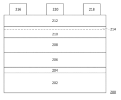
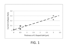
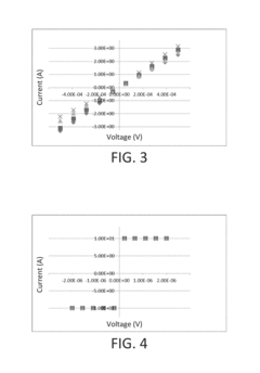
- A HEMT device with a highly resistive gallium nitride layer co-doped with carbon and a donor-type impurity, such as silicon or oxygen, is developed, where the donor-type impurity concentration is higher than carbon, maintaining a sheet resistance above 2300 Ohms/sq and suppressing undesirable defects that cause current collapse.
High electron mobility transistor (HEMT) device
PatentActiveUS10734512B2
Innovation
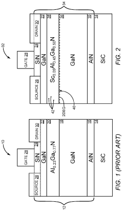
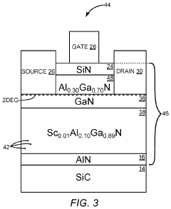
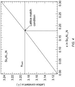
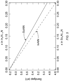
- Incorporating an aluminum (Al) based layer with a Group IIIB transition metal alloying element, such as scandium (Sc), in the epitaxial structure of HEMT devices to relieve lattice stress and maintain high sheet charge density, achieving a sheet charge density of 3.18×10^13/cm^2 with improved electron Hall mobility and reliability.
Thermal Management Considerations
Thermal management represents a critical aspect of GaN HEMT modeling for accurate circuit simulation. The high power density capabilities of GaN HEMTs, while advantageous for power applications, generate significant heat during operation that can dramatically affect device performance and reliability. Accurate thermal modeling must account for the complex heat dissipation pathways within these devices, including the thermal boundary resistances between different material layers.
Self-heating effects in GaN HEMTs manifest as temperature-dependent changes in carrier mobility, saturation velocity, and threshold voltage. These thermal dependencies create non-linear feedback loops where increased channel temperature alters electrical characteristics, which in turn affects power dissipation and further temperature rise. Conventional compact models often fail to capture these dynamic thermal behaviors, leading to significant discrepancies between simulated and actual circuit performance.
Multi-physics simulation approaches have emerged as essential tools for addressing thermal challenges in GaN HEMT modeling. These approaches couple electro-thermal simulations to account for the bidirectional relationship between electrical performance and thermal conditions. Finite element analysis (FEA) and computational fluid dynamics (CFD) techniques enable detailed thermal profile mapping across device structures, providing crucial insights for model refinement.
Recent advancements in thermal modeling include the development of distributed thermal resistance networks that more accurately represent heat flow paths in complex GaN HEMT structures. These networks incorporate both vertical and lateral thermal resistances, accounting for the anisotropic thermal conductivity of GaN and substrate materials. Dynamic thermal impedance models have also been introduced to capture transient thermal behaviors critical for pulse-mode operations common in power applications.
Temperature-dependent parameter extraction methodologies have evolved to improve model accuracy across wide operating temperature ranges. These methods typically involve characterizing device performance at multiple controlled temperatures and developing mathematical relationships that describe parameter variations with temperature. Machine learning techniques are increasingly being applied to optimize these temperature-dependent parameter models based on extensive measurement datasets.
Package-level thermal considerations must also be incorporated into comprehensive GaN HEMT models. The thermal resistance of die attach materials, package leads, and heat spreaders significantly impacts overall thermal performance. Advanced models now include package thermal networks that interface with device-level thermal models to provide end-to-end thermal simulation capabilities for circuit designers.
Reliability and Degradation Modeling
Reliability and degradation mechanisms in GaN HEMTs represent critical challenges for accurate circuit simulation models. The inherent material properties that make GaN attractive for high-power, high-frequency applications also contribute to unique degradation pathways that must be properly characterized and modeled. Current degradation modeling approaches typically focus on three primary mechanisms: hot electron effects, self-heating phenomena, and inverse piezoelectric effects.
Hot electron degradation occurs when electrons gain sufficient energy to create defects in the device structure, particularly at the AlGaN/GaN interface and in the gate region. These defects act as electron traps, altering threshold voltage and reducing channel current over time. Advanced models now incorporate time-dependent trap formation and de-trapping processes, enabling more accurate prediction of device performance degradation under various operating conditions.
Self-heating effects present another significant reliability concern, as GaN HEMTs often operate at high power densities. The thermal resistance between the active channel and heat sink significantly impacts long-term device stability. Modern thermal models have evolved from simple lumped element approaches to sophisticated 3D finite element models that account for spatial temperature distribution and material thermal boundary resistances. These models can now predict junction temperature with greater accuracy, enabling better estimation of device lifetime under various operating conditions.
Inverse piezoelectric effects, resulting from the strong piezoelectric nature of the AlGaN barrier layer, create mechanical stress under high electric fields. This stress can lead to crystallographic defects and even physical cracking of the barrier layer over time. Current models incorporate critical electric field thresholds and stress accumulation factors to predict when and where such degradation might occur.
Time-dependent dielectric breakdown (TDDB) has emerged as another critical reliability concern, particularly for gate structures. Advanced models now incorporate voltage-dependent acceleration factors and statistical Weibull distributions to predict failure probabilities across device populations rather than just individual devices.
Integration of these degradation mechanisms into compact models for circuit simulation remains challenging. Current approaches include embedding empirical degradation factors into standard compact models, developing physics-based aging models that modify key parameters over time, and creating statistical frameworks that account for device-to-device variation in degradation rates. The most promising approaches combine accelerated life testing data with physics-based understanding to create models that can extrapolate device behavior beyond test conditions to real-world operating scenarios.
Unlock deeper insights with PatSnap Eureka Quick Research — get a full tech report to explore trends and direct your research. Try now!
Generate Your Research Report Instantly with AI Agent
Supercharge your innovation with PatSnap Eureka AI Agent Platform!