

Comparison Between GaN HEMTs And SiC MOSFETs
SEP 5, 20259 MIN READ
Generate Your Research Report Instantly with AI Agent
Patsnap Eureka helps you evaluate technical feasibility & market potential.
GaN HEMTs and SiC MOSFETs Background and Development Goals
Power electronics has witnessed a significant evolution over the past decades, with silicon-based devices dominating the market for many years. However, as power systems demand higher efficiency, faster switching speeds, and operation at elevated temperatures, wide bandgap (WBG) semiconductors have emerged as promising alternatives. Among these, Gallium Nitride High Electron Mobility Transistors (GaN HEMTs) and Silicon Carbide Metal-Oxide-Semiconductor Field-Effect Transistors (SiC MOSFETs) stand out as revolutionary technologies transforming power conversion applications.
The development of GaN HEMTs traces back to the 1990s when researchers first demonstrated their potential for high-frequency applications. Initially focused on military and telecommunications applications, GaN technology has gradually expanded into power electronics. The material's wide bandgap (3.4 eV) enables devices to operate at higher voltages, temperatures, and frequencies compared to silicon counterparts.
Similarly, SiC technology has evolved significantly since the early 2000s. With a bandgap of 3.2 eV, SiC MOSFETs offer substantial improvements over traditional silicon devices in terms of breakdown voltage, thermal conductivity, and switching performance. The commercialization of SiC MOSFETs began in earnest around 2010, with continuous improvements in device performance and manufacturing processes reducing costs over time.
The technological evolution of both GaN HEMTs and SiC MOSFETs has been driven by several key factors: increasing demand for energy efficiency in power conversion systems, the push for higher power density in electronic devices, and the need for reliable operation in harsh environments. These drivers have accelerated research and development efforts across academic institutions and industry players worldwide.
Current development goals for GaN HEMTs focus on enhancing reliability, reducing costs through improved manufacturing processes, and extending voltage ratings beyond 650V for broader application in medium to high-power systems. Additionally, researchers are working to address challenges related to dynamic on-resistance and current collapse phenomena that can affect device performance.
For SiC MOSFETs, development goals include reducing on-resistance to minimize conduction losses, improving channel mobility, and enhancing gate oxide reliability. There is also significant emphasis on expanding voltage ratings up to 10kV for utility-scale applications while simultaneously driving down production costs to compete more effectively with silicon devices.
Both technologies aim to penetrate markets traditionally dominated by silicon IGBTs and MOSFETs, particularly in electric vehicles, renewable energy systems, industrial motor drives, and data center power supplies. The ultimate technical objective for both GaN HEMTs and SiC MOSFETs is to achieve an optimal balance between performance, reliability, and cost-effectiveness that enables widespread adoption across diverse power electronics applications.
Market Demand Analysis for Wide Bandgap Power Semiconductors
The wide bandgap (WBG) semiconductor market is experiencing unprecedented growth, driven by increasing demand for high-efficiency power electronics across multiple industries. The global WBG semiconductor market was valued at approximately $1.65 billion in 2022 and is projected to reach $7.5 billion by 2030, representing a compound annual growth rate (CAGR) of over 25%. This remarkable growth trajectory is fueled by the superior performance characteristics of WBG materials, particularly Gallium Nitride (GaN) and Silicon Carbide (SiC), which offer significant advantages over traditional silicon-based semiconductors.
The automotive sector represents the largest market segment for WBG semiconductors, particularly SiC MOSFETs. The electric vehicle (EV) market's explosive growth has created substantial demand for high-efficiency power conversion systems. SiC MOSFETs are increasingly being adopted in EV inverters, onboard chargers, and DC-DC converters due to their ability to operate at higher temperatures and voltages while reducing system size and weight. Major automotive manufacturers including Tesla, BMW, and Toyota have already incorporated SiC technology in their latest EV models.
Industrial applications constitute another significant market segment, with both GaN HEMTs and SiC MOSFETs finding applications in motor drives, industrial power supplies, and renewable energy systems. The industrial sector values the enhanced efficiency and reliability offered by these WBG devices, which translate to reduced operational costs and improved system performance. The market for industrial WBG applications is expected to grow at a CAGR of 22% through 2030.
Consumer electronics represents an emerging market for WBG semiconductors, particularly GaN HEMTs. The demand for smaller, faster-charging power adapters has driven adoption of GaN technology in smartphone chargers, laptop adapters, and other consumer devices. Companies like Apple, Samsung, and Anker have released GaN-based charging solutions that are significantly smaller and more efficient than their silicon counterparts. This segment is projected to grow at the fastest rate among all application areas, with a CAGR exceeding 30%.
Regional analysis reveals that Asia-Pacific currently dominates the WBG semiconductor market, accounting for approximately 45% of global demand. This is primarily due to the strong presence of semiconductor manufacturing facilities and consumer electronics production in countries like China, Japan, and South Korea. North America and Europe follow with market shares of approximately 30% and 20% respectively, driven by automotive and industrial applications.
Market challenges include the higher cost of WBG devices compared to silicon alternatives and manufacturing complexities that impact yield rates. However, as production volumes increase and manufacturing processes mature, the cost differential is expected to narrow significantly. Industry analysts predict price parity with silicon devices in certain application segments by 2026, which will further accelerate market adoption.
Technical Status and Challenges of GaN and SiC Technologies
The global power electronics market has witnessed significant advancements in wide bandgap (WBG) semiconductor technologies, with Gallium Nitride (GaN) and Silicon Carbide (SiC) emerging as frontrunners. Currently, GaN High Electron Mobility Transistors (HEMTs) have achieved remarkable progress in RF applications and are increasingly penetrating the power electronics domain, while SiC Metal-Oxide-Semiconductor Field-Effect Transistors (MOSFETs) have established a strong foothold in medium to high-power applications.
In the United States, companies like Wolfspeed, GaN Systems, and Transphorm are leading GaN and SiC development, while in Europe, STMicroelectronics and Infineon Technologies have made significant investments in WBG technologies. The Asia-Pacific region, particularly Japan with ROHM Semiconductor and China with numerous emerging players, is rapidly expanding its manufacturing capabilities and research initiatives in both technologies.
The primary technical challenges for GaN HEMTs include reliability concerns, particularly dynamic RON degradation under high-voltage switching conditions and gate reliability issues. Current collapse phenomena and buffer-related trapping effects continue to impact device performance in high-frequency applications. Additionally, the normally-on characteristic of many GaN HEMTs necessitates complex gate drive circuits, though enhancement-mode (normally-off) variants are increasingly available.
For SiC MOSFETs, the major challenges revolve around gate oxide reliability, as the interface between SiC and SiO2 exhibits higher defect densities compared to silicon devices. Channel mobility limitations and higher threshold voltage instability under high-temperature operations remain problematic. Manufacturing challenges persist, including substrate quality issues, wafer size limitations (predominantly 6-inch compared to silicon's 12-inch), and higher defect densities that impact yield and cost.
Both technologies face common challenges in packaging and thermal management. The superior switching speeds of these devices create electromagnetic interference (EMI) concerns and require advanced packaging solutions to minimize parasitic inductances. Thermal management becomes critical as these devices can operate at higher temperatures but require effective heat dissipation systems to maximize their potential.
The cost factor remains a significant barrier to widespread adoption, with both GaN and SiC devices commanding premium prices compared to silicon alternatives. However, the gap is narrowing as manufacturing processes mature and economies of scale improve. SiC technology currently enjoys greater maturity in high-power applications, while GaN excels in high-frequency, lower-voltage applications.
Standardization efforts are ongoing but remain fragmented, with different manufacturers employing varying approaches to device architecture and packaging. This lack of standardization complicates system design and integration, particularly for engineers transitioning from silicon-based solutions.
Current Technical Solutions and Implementation Approaches
01 GaN HEMT device structures and fabrication
Gallium Nitride High Electron Mobility Transistors (GaN HEMTs) feature specialized device structures that enhance performance in power applications. These structures include optimized gate designs, buffer layers, and channel formations that improve electron mobility and reduce on-resistance. Advanced fabrication techniques focus on epitaxial growth methods, surface passivation, and contact formation to minimize defects and maximize device reliability. These structural innovations enable GaN HEMTs to operate at higher frequencies and power densities compared to conventional semiconductor devices.- GaN HEMT device structures and fabrication methods: Gallium Nitride High Electron Mobility Transistors (GaN HEMTs) feature specific structural designs that enhance performance in power applications. These include specialized gate configurations, buffer layers, and channel designs that improve electron mobility and reduce on-resistance. Advanced fabrication techniques focus on epitaxial growth processes, surface treatments, and electrode formation to optimize device characteristics and reliability. These structural innovations enable GaN HEMTs to operate at higher frequencies and power densities compared to conventional semiconductor devices.
- SiC MOSFET design and manufacturing technologies: Silicon Carbide Metal-Oxide-Semiconductor Field-Effect Transistors (SiC MOSFETs) incorporate specific design elements to leverage the wide bandgap properties of SiC. Key aspects include specialized gate oxide formation techniques to address interface quality challenges, trench gate structures for reduced on-resistance, and termination designs for higher breakdown voltage. Manufacturing processes focus on substrate preparation, epitaxial growth optimization, and high-temperature annealing steps that are critical for device performance and reliability in high-power applications.
- Hybrid and integrated power modules combining GaN and SiC technologies: Hybrid power modules integrate both GaN HEMTs and SiC MOSFETs to leverage the complementary advantages of each technology. These modules feature specialized packaging solutions that address thermal management challenges, parasitic inductance reduction, and electromagnetic interference mitigation. Integration approaches include multi-chip modules, system-in-package designs, and co-packaged driver circuits. These hybrid solutions enable power conversion systems with optimized efficiency across different operating conditions, combining the high-frequency capabilities of GaN with the high-voltage robustness of SiC.
- Thermal management and reliability enhancement techniques: Advanced thermal management solutions address the high power density challenges in GaN HEMTs and SiC MOSFETs. These include novel substrate materials with enhanced thermal conductivity, advanced die-attach methods, and specialized cooling structures. Reliability enhancement techniques focus on passivation layers to mitigate surface-related degradation, field plate designs to manage electric field distribution, and buffer layer optimization to reduce leakage currents. These approaches extend device lifetime under extreme operating conditions while maintaining performance advantages over silicon-based alternatives.
- Gate driver and control circuit designs for wide bandgap devices: Specialized gate driver and control circuits are designed to address the unique switching characteristics of GaN HEMTs and SiC MOSFETs. These circuits feature high-speed switching capability, robust protection mechanisms against voltage spikes, and precise timing control to prevent shoot-through conditions. Advanced designs incorporate temperature compensation, dynamic dead-time adjustment, and active gate driving techniques that optimize switching transitions. These control solutions enable wide bandgap devices to achieve their full potential in terms of switching frequency and efficiency in power conversion applications.
02 SiC MOSFET design and manufacturing
Silicon Carbide Metal-Oxide-Semiconductor Field-Effect Transistors (SiC MOSFETs) incorporate specialized design elements to leverage the wide bandgap properties of SiC. Key design aspects include optimized gate oxide interfaces, channel doping profiles, and termination structures that enhance breakdown voltage and reduce switching losses. Manufacturing processes focus on substrate preparation, epitaxial growth techniques, and high-temperature annealing to reduce interface states and improve channel mobility. These innovations enable SiC MOSFETs to operate efficiently at higher voltages and temperatures than silicon-based alternatives.Expand Specific Solutions03 Integration and comparison of GaN and SiC power devices
Integration approaches for GaN HEMTs and SiC MOSFETs in power electronic systems leverage the complementary advantages of both technologies. Circuit topologies and driving methods are optimized for the unique switching characteristics of each device type. Comparative analyses reveal that GaN HEMTs typically offer superior high-frequency performance and lower on-resistance, while SiC MOSFETs provide better thermal stability and higher breakdown voltages. Selection criteria for specific applications consider factors such as switching frequency, operating temperature, and system cost requirements.Expand Specific Solutions04 Thermal management and reliability enhancement
Thermal management techniques for wide bandgap devices address the high power density challenges in GaN HEMTs and SiC MOSFETs. Advanced packaging solutions incorporate direct bonded copper substrates, embedded heat spreaders, and optimized die attach materials to improve heat dissipation. Reliability enhancement methods include specialized passivation layers, edge termination structures, and stress relief mechanisms to mitigate failure modes such as current collapse in GaN HEMTs and threshold voltage instability in SiC MOSFETs. Long-term reliability testing protocols are developed to accurately predict device lifetime under various operating conditions.Expand Specific Solutions05 Application-specific optimization for power conversion
GaN HEMTs and SiC MOSFETs are optimized for specific power conversion applications through tailored device parameters and circuit designs. For high-frequency converters, GaN devices are modified to minimize parasitic capacitances and gate drive requirements. For high-voltage applications, SiC MOSFETs feature enhanced edge termination and drift region designs. Application-specific driver circuits accommodate the unique switching characteristics of each device type. These optimizations enable significant improvements in power density, efficiency, and reliability across applications including electric vehicle powertrains, renewable energy systems, and industrial motor drives.Expand Specific Solutions
Key Manufacturers and Competitive Landscape Analysis
The GaN HEMT and SiC MOSFET market is currently in a growth phase, with the wide bandgap semiconductor industry expanding rapidly due to increasing demand for high-efficiency power electronics. The global market size is projected to reach $2-3 billion by 2025, growing at a CAGR of approximately 25%. Technologically, both solutions are maturing but at different rates. Companies like Wolfspeed and United Silicon Carbide have established SiC MOSFET as a more mature technology with wider commercial adoption, particularly in electric vehicles and industrial applications. Meanwhile, GaN Systems, Cambridge GaN Devices, and Innoscience are advancing GaN HEMT technology, which offers superior high-frequency performance but faces challenges in high-voltage applications. Established semiconductor players including Texas Instruments, Fujitsu, and Toshiba are investing in both technologies, indicating the strategic importance of wide bandgap semiconductors in the power electronics landscape.
Wolfspeed, Inc.
Technical Solution: Wolfspeed is a leading manufacturer of SiC MOSFETs, pioneering silicon carbide semiconductor technology. Their latest SiC MOSFET platforms deliver industry-leading efficiency with breakdown voltages ranging from 650V to 1700V. Wolfspeed's third-generation SiC MOSFETs feature optimized cell designs that reduce on-resistance by approximately 30% compared to previous generations[1]. Their C3M™ platform specifically targets high-frequency applications, achieving switching frequencies up to 500kHz while maintaining high efficiency. Wolfspeed's vertical integration approach—controlling everything from substrate production to device fabrication—ensures consistent quality and performance. Their SiC MOSFETs demonstrate superior thermal conductivity (3-4× better than GaN), allowing operation at junction temperatures up to 175°C with reliable performance[2]. The company's devices show particular strength in high-power applications like electric vehicle inverters, where their 1200V SiC MOSFETs have demonstrated efficiency improvements of 5-10% compared to silicon IGBTs[3].
Strengths: Superior thermal performance and reliability at high temperatures; established manufacturing infrastructure; higher voltage handling capability (up to 1700V); better suited for high-power applications. Weaknesses: Higher cost compared to silicon alternatives; slower switching speeds compared to GaN HEMTs; higher switching losses at very high frequencies.
GaN Systems, Inc.
Technical Solution: GaN Systems specializes in gallium nitride power transistors, focusing exclusively on enhancement-mode GaN HEMTs. Their proprietary Island Technology® creates devices with significantly reduced die size (up to 4× smaller than conventional designs) while maintaining high current capability. GaN Systems' 650V GaN transistors achieve switching frequencies exceeding 10MHz with extremely fast switching transitions—rise times under 5ns and fall times under 3ns[1]. Their GaNPX® packaging eliminates wire bonds, reducing parasitic inductance by up to 90% compared to traditional packages, which enables higher-frequency operation with minimal switching losses. The company's latest generation devices feature dynamic RDS(on) improvements of over 50%, addressing a key historical limitation of GaN technology[2]. GaN Systems has demonstrated power densities exceeding 3kW/in³ in their reference designs for applications like server power supplies, achieving efficiency improvements of 2-3% over SiC alternatives while reducing overall solution size by up to 40%[3]. Their thermal innovation includes bottom-side cooling techniques that enable effective heat dissipation despite GaN's lower thermal conductivity compared to SiC.
Strengths: Superior high-frequency performance; significantly faster switching speeds; lower switching losses; smaller form factors enabling higher power density designs; lower gate charge requirements. Weaknesses: Lower thermal conductivity than SiC; typically limited to lower voltage applications (≤650V); relatively newer technology with less field reliability data; dynamic RDS(on) effects can impact performance in some applications.
Core Patents and Technical Literature in Power Electronics
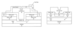
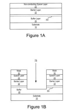
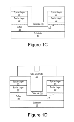
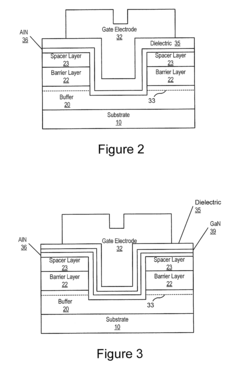
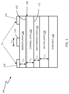
Normally-off semiconductor devices
PatentActiveUS7985986B2
Innovation
- A normally-off GaN HEMT device is developed with a Group III-nitride buffer layer, barrier layer, and non-conducting spacer layers, featuring a trench structure and gate electrode configuration that allows for low on-resistance access regions and stable threshold voltage, achieved through precise etching and layer optimization.
HIGH ELECTRON MOBILITY TRANSISTORS (HEMTS) INCLUDING A YTTRIUM (Y) AND ALUMINUM NITRIDE (AlN) (YAlN) ALLOY LAYER
PatentActiveUS20230223467A1
Innovation
- Incorporating a lattice-matched yttrium aluminum nitride (YAlN) alloy as a back-barrier layer in HEMTs, which has a wider bandgap than the gallium nitride channel layer, preventing secondary 2DEG formation and reducing thermal resistance, and can be used as an etch stop layer to improve electron confinement and gate control.
Thermal Management and Reliability Comparison
Thermal management represents a critical factor in the performance and reliability of power semiconductor devices. GaN HEMTs and SiC MOSFETs exhibit distinct thermal characteristics that significantly impact their operational capabilities in high-power applications. GaN HEMTs generally demonstrate superior thermal conductivity at the device level, with theoretical values reaching 253 W/mK compared to SiC's 370-490 W/mK. However, practical implementations reveal that GaN devices often suffer from self-heating effects due to their higher power density and smaller die sizes.
SiC MOSFETs benefit from better thermal dissipation capabilities owing to their substrate material properties. The thermal resistance (Rth) of SiC devices typically ranges from 0.5 to 1.0°C/W, while GaN HEMTs often exhibit values between 1.0 and 2.5°C/W, indicating that SiC devices can more efficiently transfer heat away from the junction. This advantage becomes particularly evident in high-current continuous operation scenarios where thermal management is paramount.
Reliability testing reveals interesting contrasts between these technologies. SiC MOSFETs demonstrate exceptional robustness under high-temperature operations, with typical maximum junction temperatures reaching 175-200°C. They also exhibit impressive long-term stability with failure rates below 10 FIT (failures in time) after 1000 hours of high-temperature reverse bias (HTRB) testing. The gate oxide reliability, however, remains a concern in extreme conditions.
GaN HEMTs present different reliability challenges. While they can theoretically operate at junction temperatures up to 250°C, practical limitations often restrict them to 150-175°C due to packaging constraints. Their dynamic Rds(on) degradation under switching conditions represents a unique reliability concern not present in SiC devices. Recent advancements in GaN technology have addressed early reliability issues, with modern devices showing mean time to failure (MTTF) exceeding 10^7 hours at 150°C.
Accelerated life testing reveals that SiC MOSFETs typically maintain stable performance characteristics after 1000 hours at elevated temperatures, with threshold voltage shifts under 100mV. GaN HEMTs, while improving, still exhibit more pronounced parametric shifts under similar conditions, particularly in terms of leakage current and dynamic on-resistance.
From a system integration perspective, thermal management strategies differ significantly between these technologies. SiC MOSFETs generally accommodate conventional cooling solutions, whereas GaN HEMTs often require more sophisticated thermal management approaches due to their higher power density and localized heating characteristics. This distinction directly impacts overall system design complexity and cooling requirements in high-power applications.
Application-Specific Performance and Cost-Benefit Analysis
When evaluating GaN HEMTs and SiC MOSFETs for specific applications, performance characteristics and cost-benefit considerations vary significantly across different sectors. In power electronics for electric vehicles (EVs), GaN HEMTs demonstrate superior switching speeds that enable higher frequency operation, resulting in smaller passive components and improved power density. However, SiC MOSFETs offer better thermal conductivity and higher voltage handling capabilities, making them preferable for high-power drivetrain applications where operating temperatures frequently exceed 150°C.
For renewable energy systems, particularly solar inverters, GaN-based solutions provide efficiency advantages at lower power levels (below 10kW), with studies showing 0.5-1% higher conversion efficiency compared to SiC alternatives. This translates to meaningful energy harvest improvements over system lifetime. Conversely, SiC MOSFETs dominate utility-scale installations where higher voltage ratings and robust short-circuit capabilities become critical operational requirements.
Telecommunications infrastructure presents another distinctive application profile. GaN HEMTs excel in RF power amplifiers and 5G base stations due to their superior high-frequency performance and lower parasitic capacitance. The resulting efficiency gains directly impact operational expenditure through reduced cooling requirements and energy consumption, with field deployments reporting 10-15% energy savings compared to conventional solutions.
From a cost-benefit perspective, the initial acquisition premium for both technologies compared to silicon alternatives (typically 2-3x higher) must be evaluated against lifetime operational savings. GaN solutions generally offer better economics in space-constrained, efficiency-critical applications below 650V, while SiC demonstrates superior cost-effectiveness in high-power, high-temperature environments above 1200V. The middle ground between 650-1200V represents a competitive battleground where application-specific requirements determine the optimal choice.
Manufacturing maturity also influences the cost-benefit equation. SiC MOSFETs benefit from more established production processes and wider supplier diversity, resulting in more stable pricing and availability. GaN HEMTs, while advancing rapidly, still face challenges in standardization and quality consistency across different manufacturers, potentially increasing implementation risks for mission-critical applications.
Total cost of ownership calculations reveal that despite higher initial component costs, both technologies can deliver 20-40% system-level cost reductions through decreased cooling requirements, smaller passive components, and improved energy efficiency. However, these benefits materialize differently across application domains, necessitating careful evaluation of specific operational parameters and design constraints.
Unlock deeper insights with Patsnap Eureka Quick Research — get a full tech report to explore trends and direct your research. Try now!
Generate Your Research Report Instantly with AI Agent
Supercharge your innovation with Patsnap Eureka AI Agent Platform!