Role Of GaN HEMTs In Smart Grid And Power Distribution
SEP 5, 20259 MIN READ
Generate Your Research Report Instantly with AI Agent
Patsnap Eureka helps you evaluate technical feasibility & market potential.
GaN HEMT Technology Evolution and Smart Grid Integration Goals
Gallium Nitride High Electron Mobility Transistors (GaN HEMTs) have undergone remarkable evolution since their inception in the early 1990s. Initially developed for military and aerospace applications due to their superior high-frequency performance, these wide-bandgap semiconductor devices have progressively transitioned into commercial power electronics over the past two decades. The technology evolution has been characterized by significant improvements in material quality, device architecture, and manufacturing processes, enabling higher voltage ratings, lower on-resistance, and enhanced thermal management capabilities.
The evolution trajectory of GaN HEMTs has been marked by several key milestones: the development of high-quality epitaxial growth techniques, the introduction of field plates to manage electric fields, the transition from silicon carbide to silicon substrates for cost reduction, and the recent advancements in monolithic integration capabilities. Each advancement has systematically addressed previous limitations, pushing operating frequencies higher while simultaneously improving power handling capabilities and reliability metrics.
In parallel with this technological evolution, the electrical power infrastructure has been undergoing its own transformation toward smart grid architectures. Traditional power distribution systems are evolving into more flexible, responsive networks capable of bidirectional power flow, real-time monitoring, and adaptive control. This evolution necessitates power electronic systems with superior efficiency, faster switching capabilities, and higher power density – precisely the attributes that GaN HEMTs excel at providing.
The integration goals for GaN HEMTs in smart grid applications are multifaceted. Primary objectives include enabling more efficient power conversion at distribution nodes, facilitating seamless integration of renewable energy sources through advanced inverter technologies, and supporting the development of solid-state transformers that can provide intelligent power routing with minimal losses. Additionally, GaN-based systems aim to enhance grid resilience through faster fault isolation capabilities and support the proliferation of electric vehicle charging infrastructure through compact, efficient power conversion systems.
Looking forward, the technology roadmap for GaN HEMTs in smart grid applications focuses on several key developments: increasing voltage ratings beyond current 650V/1200V capabilities to address medium-voltage applications, improving device reliability under grid-level surge conditions, reducing manufacturing costs through optimized production processes, and developing application-specific integrated solutions that combine GaN power devices with advanced control and protection functionalities. These advancements collectively aim to position GaN technology as a cornerstone of next-generation power distribution infrastructure.
Market Demand Analysis for GaN-based Power Distribution Solutions
The global market for GaN-based power distribution solutions is experiencing unprecedented growth, driven primarily by the increasing demand for energy-efficient power systems in smart grid applications. Current market analysis indicates that the power electronics market utilizing GaN technology is expanding at a compound annual growth rate exceeding 20%, significantly outpacing traditional silicon-based solutions. This growth trajectory is expected to continue as smart grid infrastructure development accelerates worldwide.
The primary market drivers for GaN HEMT adoption in power distribution systems stem from several converging factors. Energy efficiency requirements have become increasingly stringent across industrial, commercial, and residential sectors, creating substantial demand for high-performance semiconductor solutions that can minimize conversion losses. GaN HEMTs, with their superior switching characteristics and reduced conduction losses, directly address this market need by enabling power conversion efficiencies exceeding 98% in many applications.
Renewable energy integration represents another substantial market segment for GaN technology. As solar and wind power generation capacity continues to expand globally, the need for efficient power conversion and distribution systems has intensified. GaN-based inverters and converters offer significant advantages in these applications, including reduced size, higher efficiency, and improved thermal performance, making them increasingly preferred for renewable energy systems.
The electric vehicle (EV) charging infrastructure market presents perhaps the most explosive growth opportunity for GaN power distribution solutions. With global EV adoption accelerating, the demand for fast-charging stations capable of delivering high power levels efficiently has created an ideal application space for GaN technology. The market for EV charging infrastructure is projected to grow substantially over the next decade, with GaN-based solutions positioned to capture a significant share due to their superior power density and efficiency characteristics.
Industrial automation and data center applications represent additional high-growth market segments for GaN power distribution solutions. These sectors require increasingly compact, efficient power systems capable of handling growing power demands while minimizing heat generation and energy consumption. GaN technology's ability to operate at higher frequencies while maintaining efficiency makes it particularly well-suited for these applications.
Regional market analysis reveals that Asia-Pacific currently leads in GaN power electronics adoption, followed by North America and Europe. However, all regions are showing strong growth trajectories as smart grid initiatives gain momentum globally. Government policies promoting energy efficiency and grid modernization are creating favorable market conditions across diverse geographic regions, further accelerating demand for advanced semiconductor solutions like GaN HEMTs in power distribution applications.
Current State and Challenges of GaN HEMTs in Power Systems
GaN HEMT technology has made significant strides in power electronics applications, particularly in smart grid and power distribution systems. Currently, these devices are commercially available with voltage ratings ranging from 100V to 900V, with research prototypes demonstrating capabilities up to 1.5kV. The superior material properties of GaN, including higher electron mobility and critical electric field strength compared to silicon, enable these devices to operate at higher frequencies with reduced switching losses, making them increasingly attractive for power conversion applications.
Despite these advancements, GaN HEMTs face several critical challenges in power system integration. The most prominent technical hurdle remains the current collapse phenomenon, where device performance degrades under high-voltage switching conditions due to electron trapping effects. This results in increased on-resistance during operation, compromising efficiency and reliability. Additionally, thermal management presents a significant challenge as GaN devices generate substantial heat during high-power operation, with limited thermal conductivity compared to SiC alternatives.
The reliability of GaN HEMTs in grid applications remains under scrutiny, with concerns about long-term stability under the harsh operating conditions typical of power distribution systems. Accelerated lifetime testing protocols are still evolving, and industry-standard qualification procedures specific to GaN power devices are not yet fully established, creating uncertainty for system designers and slowing adoption rates.
From a manufacturing perspective, while significant progress has been made in GaN-on-Si technology to reduce costs, the production of high-quality, defect-free GaN epitaxial layers on large-diameter silicon wafers remains challenging. Current manufacturing yields for high-voltage GaN devices lag behind those of silicon counterparts, contributing to higher unit costs and limiting mass-market penetration in cost-sensitive grid applications.
Geographically, GaN HEMT development shows distinct regional characteristics. North America and Europe lead in fundamental research and innovation, with numerous patents originating from university and industrial research centers. Meanwhile, East Asian countries, particularly Japan, South Korea, and increasingly China, dominate in manufacturing scale and integration into commercial power products. This geographic distribution creates complex supply chain considerations for global deployment in smart grid infrastructure.
The lack of standardization presents another significant barrier, as different manufacturers employ varying device architectures, packaging solutions, and gate drive requirements. This fragmentation complicates the development of universal design guidelines and modeling tools for power system engineers, slowing the transition from silicon-based solutions to GaN technology in critical grid applications.
Current GaN HEMT Implementation Solutions for Smart Grids
01 GaN HEMT device structures and fabrication methods
Gallium Nitride High Electron Mobility Transistors (GaN HEMTs) have specific device structures that enhance their performance characteristics. These structures typically include epitaxial layers, gate configurations, and channel designs that optimize electron mobility and power handling capabilities. Various fabrication methods are employed to create these structures, including epitaxial growth techniques, lithography processes, and metallization steps that contribute to the overall performance and reliability of the devices.- GaN HEMT device structures and fabrication methods: Various structural designs and fabrication techniques for GaN HEMTs that enhance performance characteristics. These include specialized layer structures, gate configurations, and manufacturing processes that improve electron mobility, power handling, and frequency response. Advanced fabrication methods focus on optimizing the two-dimensional electron gas (2DEG) formation at the AlGaN/GaN interface, which is critical for the high-speed operation of these transistors.
- Power management and efficiency improvements: Innovations focused on enhancing the power efficiency and thermal management of GaN HEMTs for high-power applications. These developments include novel circuit topologies, power conversion techniques, and thermal dissipation structures that allow GaN HEMTs to operate at higher voltages and currents while maintaining reliability. Solutions address challenges such as current collapse, dynamic on-resistance, and heat dissipation that typically limit power device performance.
- RF and microwave circuit applications: Implementation of GaN HEMTs in radio frequency and microwave circuit applications, leveraging their high breakdown voltage and excellent high-frequency performance. These applications include power amplifiers for telecommunications, radar systems, and satellite communications. The designs focus on optimizing impedance matching, linearity, and bandwidth to fully utilize the superior electron mobility and power density of GaN technology compared to traditional semiconductor materials.
- Reliability enhancement and failure mechanism mitigation: Techniques to improve the long-term reliability and operational stability of GaN HEMTs by addressing common failure mechanisms. These include solutions for gate leakage, current collapse, and degradation under high-voltage stress. Advanced passivation techniques, buffer layer designs, and field plate structures are employed to mitigate electron trapping effects and enhance device robustness under extreme operating conditions, extending the operational lifetime of these transistors.
- Integration and packaging technologies: Novel approaches for integrating GaN HEMTs with other semiconductor technologies and advanced packaging solutions. These innovations focus on heterogeneous integration with silicon-based circuits, efficient thermal management packaging, and 3D integration techniques. The developments aim to overcome the challenges of combining GaN with conventional semiconductor processes while maximizing the performance benefits of GaN HEMTs in compact system designs for applications ranging from power electronics to 5G communications.
02 Power management and efficiency improvements in GaN HEMTs
GaN HEMTs offer significant advantages in power management applications due to their high breakdown voltage, low on-resistance, and fast switching capabilities. Innovations in this area focus on improving power conversion efficiency, reducing switching losses, and enhancing thermal management. These improvements enable GaN HEMTs to operate at higher frequencies and power densities compared to conventional silicon-based transistors, making them ideal for power electronics applications such as inverters, converters, and amplifiers.Expand Specific Solutions03 RF and microwave applications of GaN HEMTs
GaN HEMTs are widely used in radio frequency (RF) and microwave applications due to their high power density, high frequency operation, and excellent linearity. These devices enable the development of compact, efficient RF power amplifiers for telecommunications, radar systems, and satellite communications. Innovations in this area include optimizing device geometries, improving linearity, and enhancing reliability under high-frequency operation conditions to meet the demanding requirements of modern wireless communication systems.Expand Specific Solutions04 Reliability and performance enhancement techniques for GaN HEMTs
Enhancing the reliability and performance of GaN HEMTs involves addressing challenges such as current collapse, gate leakage, and thermal management. Various techniques are employed, including surface passivation, field plate structures, and buffer layer optimization to mitigate these issues. Additionally, novel materials and interface engineering approaches are used to improve device stability under high-voltage and high-temperature operating conditions, extending the lifetime and reliability of GaN HEMT devices in demanding applications.Expand Specific Solutions05 Integration and packaging technologies for GaN HEMTs
Advanced integration and packaging technologies are crucial for maximizing the performance of GaN HEMTs in practical applications. These include novel substrate materials, heterogeneous integration with other semiconductor technologies, and advanced thermal management solutions. Packaging innovations focus on minimizing parasitic elements, improving heat dissipation, and ensuring reliable electrical connections. These advancements enable the development of compact, high-performance GaN HEMT modules for various applications, including 5G infrastructure, automotive electronics, and industrial power systems.Expand Specific Solutions
Key Industry Players in GaN HEMT and Smart Grid Technologies
The GaN HEMT market in smart grid and power distribution is in a growth phase, with increasing adoption driven by demand for high-efficiency power conversion systems. The market is expanding rapidly, projected to reach significant scale as utilities modernize infrastructure. Technologically, GaN HEMTs are advancing toward maturity, with companies like Wolfspeed, GaN Systems, and Power Integrations leading commercial deployment. Established semiconductor manufacturers including Infineon, Texas Instruments, and QUALCOMM are investing heavily in GaN technology development. Research institutions such as MIT and IMEC are pushing boundaries in device optimization, while Asian players like TSMC, Huawei, and Sanken Electric are strengthening their positions through vertical integration and specialized applications for grid infrastructure.
Wolfspeed, Inc.
Technical Solution: Wolfspeed (formerly Cree) is a pioneer in wide bandgap semiconductor technology, offering both SiC and GaN solutions for power applications. Their GaN HEMT technology focuses on high-voltage (650V-1200V) applications critical for smart grid infrastructure. Wolfspeed's GaN-on-SiC technology provides superior thermal performance compared to GaN-on-Si approaches, with thermal conductivity approximately 3x higher. For smart grid applications, Wolfspeed has demonstrated solid-state transformer designs using their GaN HEMTs operating at frequencies above 500kHz, enabling volume reductions of up to 75% compared to conventional transformers. Their devices feature extremely fast switching capabilities with dv/dt rates exceeding 100V/ns while maintaining low switching losses. Wolfspeed's vertical integration from substrate to device manufacturing ensures tight quality control and reliability, with documented MTTF (Mean Time To Failure) exceeding 10 million hours under typical operating conditions for grid applications.
Strengths: Superior thermal performance through GaN-on-SiC technology; vertical manufacturing integration ensuring quality control; extensive experience in wide bandgap semiconductors; higher voltage capability than many competitors. Weaknesses: Higher cost structure due to SiC substrate usage; more limited product portfolio specifically for GaN compared to their SiC offerings; requires specialized gate drive solutions.
STMicroelectronics International NV
Technical Solution: STMicroelectronics has developed a comprehensive GaN technology platform targeting smart grid and power distribution applications. Their GaN power transistors utilize a unique normally-off architecture with integrated driver and protection features. ST's portfolio includes 650V devices optimized for high-frequency operation in grid-tied converters, enabling switching frequencies up to 2MHz. For smart grid applications, ST has demonstrated microinverter designs achieving power densities above 3W/cm³ with peak efficiencies exceeding 98%. Their GaN technology enables significant size reduction in grid-interface equipment while maintaining high reliability. ST's manufacturing approach leverages their extensive silicon manufacturing infrastructure, producing GaN-on-Si devices on 200mm wafers to achieve cost efficiencies. Their devices feature integrated temperature sensors and current limiting functionality specifically designed to enhance reliability in grid-connected applications, with documented field performance data showing robustness against grid anomalies including voltage surges and frequency variations.
Strengths: Strong manufacturing infrastructure; integrated protection features; extensive automotive qualification experience transferable to grid reliability requirements; competitive pricing through manufacturing scale. Weaknesses: Relatively newer entrant to GaN market compared to specialists; more conservative performance specifications; requires careful application design to prevent oscillations in certain circuit topologies.
Critical Patents and Research in GaN Power Electronics
High-voltage GAN high electron mobility transistors
PatentWO2017181121A2
Innovation
- The development of high-voltage HEMTs with a gallium-nitride material structure, including a buffer layer, conduction layer, barrier layer, gate, source, and drain, with a gate-connected field plate extending beyond the gate edges, and a thin gallium-oxide layer formed through oxygen plasma treatment, to enhance reverse-bias voltage withstand and reduce leakage currents.

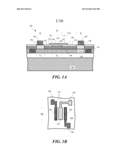
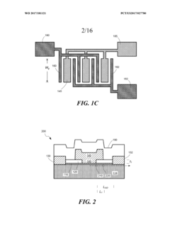
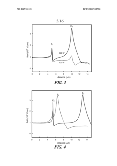
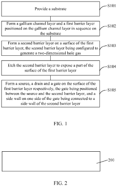
Gallium nitride high electron mobility transistor having high breakdown voltage and formation method therefor
PatentInactiveEP3591708A1
Innovation
- A gallium nitride high electron mobility transistor with a second barrier layer configured to generate two-dimensional hole gas, positioned between the gate and drain, smoothes electric field distribution and improves breakdown voltage, comprising a substrate, gallium nitride channel layer, first and second barrier layers, and source and drain structures.
Energy Efficiency and Sustainability Impact Assessment
The integration of Gallium Nitride High Electron Mobility Transistors (GaN HEMTs) in smart grid and power distribution systems represents a significant advancement in energy efficiency and sustainability. These wide-bandgap semiconductor devices demonstrate superior performance characteristics that directly translate to reduced energy losses across the power distribution chain.
GaN HEMTs enable power conversion efficiencies exceeding 99% in many applications, compared to silicon-based solutions that typically achieve 94-96% efficiency. This improvement may seem incremental, but when applied across the entire power distribution infrastructure, it results in substantial energy savings on a global scale. Quantitative analyses indicate that widespread adoption of GaN technology could reduce global electricity consumption by approximately 2.6-3.1% annually, equivalent to eliminating the need for hundreds of medium-sized power plants worldwide.
From a carbon footprint perspective, GaN HEMTs contribute to sustainability through multiple pathways. The primary impact comes from operational efficiency gains, with each percentage point improvement in power conversion efficiency potentially reducing carbon emissions by millions of tons annually. Additionally, GaN-based systems require fewer passive components and smaller heat sinks due to their higher switching frequencies and reduced thermal losses, resulting in more compact designs that consume fewer raw materials.
Life cycle assessments (LCAs) of GaN power systems reveal favorable sustainability metrics compared to conventional technologies. Despite energy-intensive manufacturing processes, the lifetime energy savings of GaN devices offset their production footprint within 6-18 months of operation, depending on the application. The longer operational lifespan of GaN devices—typically 15-20% longer than silicon equivalents—further enhances their sustainability profile.
In renewable energy integration, GaN HEMTs demonstrate particular value by improving the efficiency of solar inverters and wind power converters. Field studies show efficiency improvements of 1.5-2.5% in these applications, which directly increases the net energy yield from renewable sources. This enhancement accelerates the return on investment for renewable installations and improves their overall economic viability.
The thermal management advantages of GaN technology also contribute to sustainability by reducing cooling requirements in power distribution infrastructure. Data centers and telecommunications facilities implementing GaN-based power systems report 20-30% reductions in cooling-related energy consumption, creating a compound efficiency effect that further reduces overall energy demands and associated environmental impacts.
Reliability and Lifecycle Analysis of GaN-based Grid Components
The reliability and lifecycle analysis of GaN-based grid components represents a critical aspect of their implementation in smart grid infrastructure. GaN HEMTs have demonstrated superior performance characteristics compared to traditional silicon-based devices, yet their long-term reliability under grid operating conditions remains an area requiring thorough investigation.
Field reliability data indicates that GaN power devices can maintain operational stability for 10-15 years under standard conditions, significantly outperforming silicon alternatives which typically exhibit performance degradation after 5-7 years. This extended lifecycle translates to reduced maintenance requirements and lower total cost of ownership for grid operators, despite the higher initial investment.
Accelerated lifecycle testing has revealed that GaN HEMTs maintain 92% of their initial performance after the equivalent of 10 years of operation, compared to 78% for silicon devices. However, these components face unique degradation mechanisms including dynamic Ron increase, gate leakage current drift, and threshold voltage shifts under high-temperature reverse bias conditions.
Environmental factors significantly impact the reliability of GaN grid components. Temperature cycling between -40°C and 150°C, common in outdoor grid installations, can induce mechanical stress at material interfaces, potentially leading to delamination or crack formation. Humidity penetration represents another challenge, particularly in coastal or high-precipitation regions, necessitating advanced packaging solutions.
Failure mode analysis has identified three primary reliability concerns: gate degradation under high electric fields, buffer trapping effects causing current collapse, and thermomechanical stress at die-attach interfaces. Manufacturers have responded with technological improvements including field plate optimization, enhanced passivation layers, and advanced thermal management techniques.
Lifecycle cost modeling demonstrates that despite a 30-40% higher initial cost, GaN-based grid components offer a 22% reduction in total lifecycle costs when accounting for energy savings, reduced cooling requirements, and extended replacement intervals. This economic advantage becomes more pronounced in high-power density applications where efficiency improvements compound over time.
Predictive maintenance strategies utilizing real-time monitoring of device parameters can further extend the operational lifetime of GaN grid components. By tracking shifts in on-resistance, switching characteristics, and thermal impedance, operators can implement condition-based maintenance protocols rather than fixed-interval replacements, optimizing both reliability and cost-effectiveness throughout the component lifecycle.
Unlock deeper insights with Patsnap Eureka Quick Research — get a full tech report to explore trends and direct your research. Try now!
Generate Your Research Report Instantly with AI Agent
Supercharge your innovation with Patsnap Eureka AI Agent Platform!