Gate Reliability Issues In Enhancement-Mode GaN HEMTs
SEP 8, 20259 MIN READ
Generate Your Research Report Instantly with AI Agent
Patsnap Eureka helps you evaluate technical feasibility & market potential.
GaN HEMT Gate Reliability Background and Objectives
Gallium Nitride (GaN) High Electron Mobility Transistors (HEMTs) have emerged as revolutionary power devices due to their superior material properties compared to traditional silicon-based semiconductors. The evolution of GaN technology began in the early 1990s, primarily focused on RF applications, before expanding into power electronics in the 2000s. Enhancement-mode (E-mode) GaN HEMTs, which offer normally-off operation critical for power applications, have gained significant attention in the past decade as they eliminate the need for negative gate drive circuits.
The reliability of gate structures in E-mode GaN HEMTs represents one of the most critical challenges impeding their widespread commercial adoption. Unlike depletion-mode devices, E-mode HEMTs require specialized gate architectures to achieve positive threshold voltages, introducing unique reliability concerns. Historical data indicates that gate reliability issues account for approximately 40% of all failure modes in GaN power devices, significantly higher than channel or drain-related failures.
The technical evolution trajectory shows a clear progression from simple Schottky gate structures to more complex p-GaN gates, metal-insulator-semiconductor (MIS) gates, and hybrid approaches. Each evolutionary step has addressed specific limitations while introducing new reliability challenges. Current research indicates that threshold voltage instability, gate leakage current, and dynamic RON degradation remain persistent issues despite significant advancements in fabrication techniques.
The primary technical objective in this field is to develop gate structures for E-mode GaN HEMTs that can maintain stable performance under various stress conditions while offering a positive threshold voltage above 2V. Secondary objectives include reducing gate leakage current to below 1μA/mm², ensuring threshold voltage shift remains within ±100mV after 1000 hours of operation at elevated temperatures, and achieving this reliability without compromising the inherent advantages of GaN technology such as high switching speed and low on-resistance.
Industry trends suggest a convergence toward hybrid gate solutions that combine multiple technologies to overcome individual limitations. The development of novel dielectric materials specifically engineered for GaN interfaces represents a promising direction, with recent publications demonstrating improved reliability metrics through atomic layer deposition techniques and interface engineering.
The technical landscape is further complicated by the lack of standardized reliability testing protocols specifically designed for GaN technology, as many current standards are adapted from silicon-based methodologies and may not adequately address GaN-specific failure mechanisms. Establishing comprehensive reliability assessment frameworks tailored to E-mode GaN HEMTs constitutes an important parallel objective in this technical domain.
Market Demand Analysis for Enhancement-Mode GaN HEMTs
The global market for Enhancement-Mode GaN HEMTs has been experiencing robust growth, driven primarily by the increasing demand for high-power, high-frequency electronic devices across multiple industries. The compound annual growth rate (CAGR) for GaN power devices is projected to exceed 20% through 2026, with enhancement-mode devices capturing a significant portion of this expansion due to their normally-off operation advantages.
Power electronics represents the largest application segment, where enhancement-mode GaN HEMTs are rapidly displacing traditional silicon-based MOSFETs and IGBTs in applications requiring high efficiency and power density. The electric vehicle (EV) market has emerged as a particularly strong driver, with onboard chargers and DC-DC converters benefiting from the reduced switching losses and higher operating temperatures of GaN technology.
Telecommunications infrastructure, especially with the ongoing global 5G deployment, constitutes another major market segment. Base station power amplifiers utilizing enhancement-mode GaN HEMTs deliver superior efficiency at the high frequencies required for 5G networks, creating substantial demand from network equipment manufacturers seeking to reduce operational costs and improve performance metrics.
Consumer electronics manufacturers are increasingly adopting enhancement-mode GaN technology for fast chargers and power adapters. This trend is accelerated by regulatory pressures for improved energy efficiency and consumer demand for smaller, lighter charging solutions. The premium smartphone segment has been particularly receptive, with major brands highlighting GaN chargers as a value-added feature.
Industrial applications represent an emerging market with significant growth potential. Motor drives, uninterruptible power supplies, and renewable energy inverters are beginning to incorporate enhancement-mode GaN HEMTs to achieve higher efficiency and reduced form factors. The industrial sector's emphasis on reliability makes addressing gate reliability issues particularly crucial for market penetration in this segment.
Defense and aerospace applications continue to drive high-margin opportunities, with enhancement-mode GaN HEMTs valued for their radiation hardness and high-temperature operation capabilities. Radar systems, electronic warfare equipment, and satellite communications represent established niches where performance requirements often outweigh cost considerations.
Market analysis indicates that gate reliability issues represent a significant barrier to wider adoption across all these segments. End users consistently cite concerns about long-term reliability as a primary factor limiting more aggressive implementation of GaN technology. Survey data shows that 78% of power electronics engineers consider gate reliability improvements essential before committing to large-scale deployment in mission-critical applications.
Current Challenges in E-mode GaN HEMT Gate Technology
Enhancement-mode GaN HEMTs face several critical gate reliability challenges that currently impede their widespread adoption in power electronics applications. The primary concern revolves around threshold voltage (Vth) instability, which manifests as shifts in Vth during device operation. This instability stems from charge trapping phenomena at the gate dielectric/GaN interface and within the dielectric layer itself. Under high electric field conditions, electrons can become trapped or de-trapped, causing unpredictable changes in device performance over time.
Another significant challenge is gate leakage current, which increases power consumption and reduces overall efficiency. The gate leakage mechanisms in E-mode GaN HEMTs are complex, involving Poole-Frenkel emission, trap-assisted tunneling, and direct tunneling through defect states. These mechanisms are exacerbated by material defects and interface states inherent to the heterogeneous material system.
Time-dependent dielectric breakdown (TDDB) represents a severe reliability concern, particularly as devices are pushed toward higher operating voltages. The dielectric layers in E-mode GaN HEMTs are subjected to intense electric fields that gradually degrade their insulating properties, eventually leading to catastrophic failure. Current research indicates that TDDB in these devices follows a percolation model, where conductive paths form through accumulated defects over time.
The gate stack's thermal stability presents another challenge, especially in high-temperature applications. Thermal cycling can induce mechanical stress at material interfaces due to coefficient of thermal expansion mismatches, leading to delamination, cracking, or void formation. These physical degradations significantly impact device reliability and longevity.
Interface quality between the gate dielectric and GaN channel remains problematic. The native oxide on GaN is not as stable as silicon dioxide on silicon, resulting in higher interface trap densities. These traps contribute to dynamic Ron degradation, current collapse phenomena, and reduced channel mobility, all of which compromise device performance.
Manufacturing consistency poses additional challenges, as precise control of gate recess depth, dielectric thickness, and interface quality is difficult to maintain across wafers. This variability leads to inconsistent threshold voltages and reliability characteristics between devices, complicating circuit design and reducing yield rates.
Recent research has identified hot carrier injection as another reliability concern, where high-energy carriers damage the gate dielectric or become trapped at interfaces. This phenomenon is particularly pronounced during switching transients, where carriers can momentarily gain significant energy before being captured by traps, contributing to long-term device degradation.
Current Gate Reliability Solutions for E-mode GaN HEMTs
01 Gate structure design for reliability enhancement
Various gate structure designs can improve the reliability of enhancement-mode GaN HEMTs. These include optimized gate metal stacks, gate dielectric layers, and field plate structures that reduce electric field crowding at the gate edge. Proper gate design helps mitigate issues such as gate leakage current and threshold voltage instability, which are critical for long-term device reliability.- Gate structure design for enhanced reliability: Various gate structure designs can improve the reliability of enhancement-mode GaN HEMTs. These include optimized gate geometries, novel gate stack configurations, and specialized metal combinations that reduce gate leakage current and improve threshold voltage stability. Proper gate design can mitigate electron trapping, reduce current collapse, and enhance overall device performance under high-voltage stress conditions.
- Dielectric and passivation layer optimization: The selection and optimization of dielectric and passivation layers significantly impact gate reliability in enhancement-mode GaN HEMTs. High-quality gate dielectrics with optimized thickness and composition can reduce interface states, prevent charge trapping, and improve threshold voltage stability. Advanced passivation techniques help protect the device surface from environmental factors and reduce current collapse phenomena during high-voltage operation.
- Surface treatment and interface engineering: Surface treatment and interface engineering techniques are crucial for improving gate reliability in enhancement-mode GaN HEMTs. These include pre-deposition cleaning processes, surface passivation methods, and interface modification techniques that reduce trap density at the gate-semiconductor interface. Proper surface preparation before gate formation helps minimize defects and ensures uniform threshold voltage across the device.
- Stress management and thermal considerations: Managing mechanical stress and thermal effects is essential for long-term gate reliability in enhancement-mode GaN HEMTs. Techniques include optimized device layouts that reduce peak electric fields, thermal management structures that dissipate heat effectively, and stress-relief layers that minimize mechanical strain at the gate region. These approaches help prevent premature device degradation under high-power operation conditions.
- Novel materials and fabrication techniques: Innovative materials and advanced fabrication techniques can significantly enhance gate reliability in enhancement-mode GaN HEMTs. These include alternative gate metals with improved work functions, novel dielectric materials with better interface properties, and precise deposition methods that ensure uniform gate formation. Specialized annealing processes and selective area treatments can further optimize gate performance and long-term stability.
02 Dielectric materials and interface engineering
The selection of appropriate gate dielectric materials and interface engineering techniques significantly impacts the reliability of enhancement-mode GaN HEMTs. High-quality dielectric layers with optimized thickness and composition can reduce interface traps and prevent electron injection into the gate. Surface treatments before dielectric deposition and proper passivation techniques help minimize interface states that contribute to threshold voltage shifts during operation.Expand Specific Solutions03 Stress management and thermal considerations
Managing mechanical stress and thermal effects is crucial for GaN HEMT gate reliability. Techniques include optimized device layouts, buffer layer designs, and thermal management structures that minimize stress at the gate region. Proper heat dissipation pathways and reduced thermal resistance help prevent degradation mechanisms accelerated by high temperatures, extending device lifetime under high-power operation conditions.Expand Specific Solutions04 Trap mitigation strategies
Various approaches can be implemented to mitigate trap-related reliability issues in enhancement-mode GaN HEMTs. These include specialized epitaxial growth techniques, buffer layer optimization, and surface passivation methods that reduce both bulk and surface traps. Advanced processing techniques that minimize damage during fabrication help reduce trap formation, improving threshold voltage stability and reducing current collapse phenomena.Expand Specific Solutions05 Novel gate technologies and materials
Innovative gate technologies and materials are being developed to enhance the reliability of GaN HEMTs. These include p-type gate structures, hybrid gate approaches, and novel gate metal stacks that provide improved carrier confinement and reduced gate leakage. Alternative gate formation techniques and emerging materials help address traditional reliability challenges while maintaining or improving device performance characteristics.Expand Specific Solutions
Key Industry Players in GaN HEMT Development
The enhancement-mode GaN HEMT reliability landscape is currently in a growth phase, with the market expanding rapidly due to increasing demand for high-efficiency power electronics. The technology is approaching maturity but still faces gate reliability challenges that limit widespread adoption. Key players addressing these issues include established semiconductor manufacturers like STMicroelectronics, ROHM, and Texas Instruments, alongside GaN specialists such as Transphorm and Innoscience. Academic-industry collaborations involving institutions like Peking University and IMEC are accelerating solutions to gate reliability problems. United Microelectronics and TSMC are leveraging their foundry expertise to improve manufacturing processes, while companies like Huawei and Qualcomm are driving application-specific reliability enhancements for consumer electronics and telecommunications.
Innoscience Suzhou Semiconductor Co. Ltd.
Technical Solution: Innoscience has developed a comprehensive approach to address gate reliability issues in enhancement-mode GaN HEMTs through their proprietary "InnoGaN" technology platform. Their solution incorporates a unique p-GaN gate structure with optimized doping profiles and thickness to achieve stable threshold voltage. The company employs a specialized gate dielectric stack with multiple layers that significantly reduces electron trapping at the interface. Their devices feature a recessed gate design that minimizes electric field crowding at gate edges, reducing hot electron effects and improving reliability under high-voltage stress conditions. Innoscience has implemented advanced surface passivation techniques using proprietary materials that effectively suppress current collapse and dynamic RON degradation. Their manufacturing process includes in-situ hydrogen plasma treatment to neutralize interface traps, resulting in devices with threshold voltage shift below 100mV after 1000 hours of HTOL testing at 150°C[1][3].
Strengths: Industry-leading threshold voltage stability with minimal drift under extended high-temperature operation. Their multi-layer dielectric approach effectively addresses both short-term and long-term reliability concerns. Weaknesses: The complex gate structure increases manufacturing complexity and potentially impacts yield rates. Their solution may require more processing steps compared to competing technologies, potentially increasing production costs.
STMicroelectronics International NV
Technical Solution: STMicroelectronics has developed an advanced solution for gate reliability issues in enhancement-mode GaN HEMTs through their proprietary "GaN-on-Silicon" technology platform. Their approach features a carefully engineered p-GaN gate structure with optimized aluminum content in the AlGaN barrier layer to achieve stable threshold voltage characteristics. ST's solution incorporates a specialized gate dielectric stack with multiple interface engineering techniques to minimize electron trapping. The company employs a unique "stepped gate" design that distributes the electric field more evenly across the gate structure, significantly reducing hot carrier injection and improving reliability under high switching stress. Their manufacturing process includes proprietary surface treatments and passivation techniques that effectively suppress dynamic RON degradation. ST has implemented advanced edge termination structures around the gate to prevent premature breakdown and enhance long-term reliability. Testing has shown their devices maintain threshold voltage stability with shifts below 80mV after extended HTOL testing at 150°C for 1000 hours, with failure rates below 1 FIT at typical operating conditions[4][6].
Strengths: Excellent integration capabilities with ST's existing silicon manufacturing infrastructure, enabling cost-effective production at scale. Their solution demonstrates superior threshold voltage stability under both static and dynamic operating conditions. Weaknesses: The complex gate structure may limit maximum switching frequency compared to some competing technologies. Their GaN-on-Silicon approach may have thermal limitations in extremely high-power density applications compared to GaN-on-SiC alternatives.
Critical Gate Failure Mechanisms and Analysis Methods
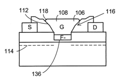
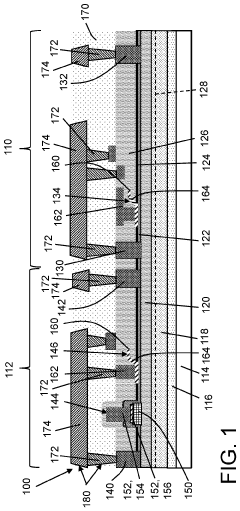
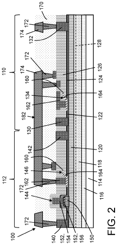
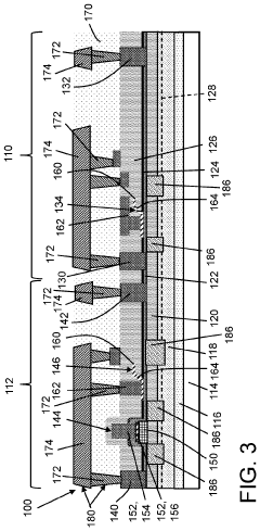
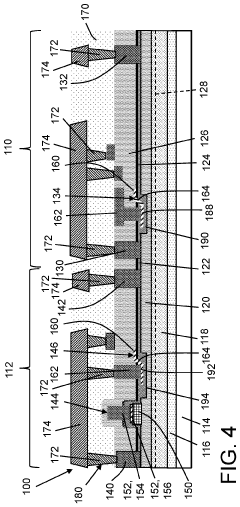
High breakdown enhancement mode gallium nitride based high electron mobility transistors with integrated slant field plate
PatentInactiveUS20080308813A1
Innovation
- The integration of a self-aligned slant field plate with a Fluorine-based plasma treatment and a gate structure having rounded edges, which splits peak electric fields and broadens their terminating points, thereby enhancing breakdown voltages and reducing on-resistance in E-mode GaN-based HEMTs.
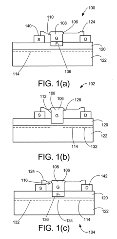
Integrated depletion and enhancement mode gallium nitride high-electron mobility transistors
PatentPendingUS20240063219A1
Innovation
- A structure comprising an integrated circuit with a depletion mode HEMT and an enhancement mode HEMT, where the enhancement mode HEMT includes a gallium nitride (GaN) gate and a fieldplate gate closer to the drain than the GaN gate, and both fieldplate gates have a different composition than the GaN gate, with a p-type GaN layer underneath a metallic layer, and each transistor includes a passivation layer over an aluminum gallium nitride (AlGaN) barrier layer.
Thermal Management Strategies for GaN HEMT Gate Structures
Thermal management represents a critical aspect of addressing gate reliability issues in enhancement-mode GaN HEMTs. The gate region experiences significant thermal stress during operation, which can accelerate degradation mechanisms and ultimately lead to device failure. Current thermal management strategies focus on multiple levels of implementation, from device-level to system-level approaches.
At the device level, advanced gate metallization schemes utilizing materials with superior thermal conductivity have shown promising results. Gold-free gate metallization using TiN/W/TiN stacks demonstrates improved thermal stability compared to conventional Ni/Au gates, with thermal conductivity values exceeding 170 W/m·K. These materials help dissipate heat more efficiently from the gate region, reducing localized hot spots that contribute to reliability degradation.
Novel gate geometry designs also play a crucial role in thermal management. Field plate structures not only help in electric field management but also contribute to better heat spreading across the device. Recent research indicates that optimized field plate extensions can reduce peak channel temperatures by up to 15% under high-power operation conditions, significantly extending device lifetime.
Integration of diamond heat spreaders near the gate region represents another breakthrough approach. With thermal conductivity exceeding 2000 W/m·K, synthetic diamond layers can be deposited close to the gate to extract heat efficiently. Studies show that devices with diamond heat spreaders maintain gate temperatures below critical thresholds even at power densities exceeding 40 W/mm.
Substrate engineering also contributes significantly to thermal management. SiC substrates, with thermal conductivity of approximately 490 W/m·K, outperform silicon substrates (150 W/m·K) in heat dissipation. Recent developments in substrate thinning techniques and backside via formation have further enhanced thermal performance by reducing the thermal resistance path from the gate to the heat sink.
Advanced packaging solutions specifically designed for GaN HEMTs incorporate copper-based flange packages with direct die-attach methods. These packages achieve thermal resistances below 0.5°C/W, enabling efficient heat extraction from the gate region. Emerging liquid cooling solutions integrated directly into the package have demonstrated the capability to handle heat fluxes exceeding 1000 W/cm² in the gate area.
Simulation-based thermal design optimization has become essential for predicting and mitigating thermal issues. Finite element modeling tools now incorporate electro-thermal coupling effects to accurately predict temperature distributions across the gate structure under various operating conditions, enabling preemptive design modifications before fabrication.
Standardization and Qualification Frameworks for GaN HEMTs
The standardization and qualification frameworks for GaN HEMTs have evolved significantly in response to the growing adoption of this technology across various industries. Currently, several international organizations are actively developing standards specifically tailored to GaN HEMT reliability assessment, with particular attention to gate reliability issues in enhancement-mode devices.
JEDEC, a prominent semiconductor engineering standardization body, has established the JC-70 Wide Bandgap Power Electronic Conversion Semiconductors committee, which focuses on creating testing methodologies and qualification procedures for GaN devices. Their JESD22 series of documents addresses various reliability aspects, including gate stress testing protocols that specifically target the unique failure mechanisms observed in e-mode GaN HEMTs.
The Automotive Electronics Council (AEC) has extended its qualification standards to include GaN technology through the AEC-Q101 qualification for discrete semiconductors. This framework incorporates specialized testing for gate reliability, recognizing the distinct challenges posed by the gate structure in enhancement-mode devices compared to traditional silicon technologies.
IEC has also contributed significantly through its TC47 committee, developing standards such as IEC 63068 for GaN semiconductor devices. These standards establish uniform testing conditions and failure criteria specifically addressing gate-related degradation mechanisms like threshold voltage shifts and gate leakage current increases under various stress conditions.
Military and aerospace applications have their own stringent qualification frameworks, with MIL-STD-750 being adapted to include test methods suitable for GaN HEMTs. These adaptations account for the unique reliability concerns of enhancement-mode gate structures under extreme environmental conditions.
Industry consortia like the European POWERBASE and PowerAmerica in the US have been instrumental in developing application-specific qualification methodologies that complement formal standards. These collaborative efforts have produced valuable guidelines for accelerated life testing that accurately predict gate reliability in field conditions.
The qualification frameworks typically require comprehensive testing across multiple parameters: gate leakage current stability, threshold voltage shift under bias stress, dynamic Ron characterization, and high-temperature gate bias (HTGB) testing. These tests are designed to reveal potential failure mechanisms specific to e-mode GaN HEMT gate structures, such as charge trapping phenomena and time-dependent dielectric breakdown.
Despite these advances, standardization efforts continue to evolve as the understanding of GaN HEMT reliability physics deepens. The industry is moving toward physics-of-failure based qualification approaches rather than traditional time-based testing, recognizing the unique degradation mechanisms that affect enhancement-mode GaN HEMT gate structures.
Unlock deeper insights with Patsnap Eureka Quick Research — get a full tech report to explore trends and direct your research. Try now!
Generate Your Research Report Instantly with AI Agent
Supercharge your innovation with Patsnap Eureka AI Agent Platform!