Cost Trends And Market Adoption Of GaN HEMT Technology
SEP 5, 20259 MIN READ
Generate Your Research Report Instantly with AI Agent
Patsnap Eureka helps you evaluate technical feasibility & market potential.
GaN HEMT Technology Evolution and Objectives
Gallium Nitride High Electron Mobility Transistor (GaN HEMT) technology has evolved significantly since its inception in the early 1990s, transforming from a laboratory curiosity to a commercial reality. The technology leverages the wide bandgap properties of GaN, which enables higher breakdown voltages, faster switching speeds, and superior thermal performance compared to traditional silicon-based semiconductors. This evolution has been driven by increasing demands for higher power density, efficiency, and frequency performance in various applications.
The initial development phase of GaN HEMT technology focused primarily on military and defense applications, particularly for radar and communication systems. During this period, research concentrated on understanding the fundamental material properties and device physics of GaN heterostructures. By the early 2000s, significant progress had been made in epitaxial growth techniques, particularly metal-organic chemical vapor deposition (MOCVD), which enabled the production of high-quality GaN layers on various substrates.
A pivotal advancement came with the development of GaN-on-Silicon technology around 2005-2010, which dramatically reduced substrate costs compared to traditional sapphire or silicon carbide substrates. This innovation marked a turning point for commercial viability, opening doors to mass-market applications beyond the defense sector. Subsequently, improvements in device reliability, particularly addressing issues like current collapse and gate leakage, further accelerated market adoption.
The technology evolution trajectory has been characterized by continuous improvements in power handling capability, efficiency, and reliability. Modern GaN HEMTs now routinely achieve power densities exceeding 5 W/mm at microwave frequencies, with breakdown voltages above 100V, and power-added efficiencies approaching 70% in certain configurations. These performance metrics represent orders of magnitude improvement over the first-generation devices.
Current technical objectives for GaN HEMT technology focus on several key areas. Cost reduction remains paramount, with efforts directed toward improving yield, reducing epitaxial layer complexity, and optimizing manufacturing processes. Integration challenges are being addressed through advanced packaging solutions and monolithic integration with drive and control circuitry. Reliability enhancement continues to be critical, with research targeting degradation mechanisms and developing robust passivation techniques.
Looking forward, the technology roadmap aims to expand the frequency range of operation into millimeter-wave bands for 5G and beyond, increase power handling capabilities for electric vehicle and renewable energy applications, and further reduce costs to enable penetration into consumer electronics markets. The ultimate objective is to position GaN HEMT technology as the dominant solution for high-frequency, high-power applications across multiple industries, displacing legacy silicon and GaAs technologies where performance advantages justify the cost premium.
Market Demand Analysis for GaN HEMT Solutions
The global market for GaN HEMT (Gallium Nitride High Electron Mobility Transistor) technology has witnessed substantial growth in recent years, driven primarily by increasing demands in power electronics, RF applications, and telecommunications infrastructure. Market research indicates that the GaN power device market is expected to reach $1.75 billion by 2026, growing at a CAGR of approximately 35% from 2021 to 2026.
The telecommunications sector represents the largest market segment for GaN HEMT technology, particularly with the ongoing global deployment of 5G infrastructure. Network operators are increasingly adopting GaN-based power amplifiers due to their superior efficiency and bandwidth capabilities compared to traditional silicon-based solutions. This transition has been accelerated by the need for higher data rates and expanded network coverage, creating a sustained demand growth of nearly 40% annually in this segment alone.
Defense and aerospace applications form another significant market for GaN HEMT technology. Military radar systems, electronic warfare equipment, and satellite communications increasingly rely on GaN HEMTs for their high-power density and reliability under extreme conditions. The defense sector's demand for GaN technology has grown steadily at 25% annually, with government contracts and defense modernization programs serving as key market drivers.
Consumer electronics represents an emerging but rapidly expanding market for GaN HEMT solutions. The fast-charging segment for mobile devices and laptops has seen particularly strong adoption, with GaN-based chargers offering significantly smaller form factors and higher efficiency than silicon alternatives. Market penetration in consumer electronics has doubled each year since 2019, with over 50 million GaN chargers shipped in 2022 alone.
Automotive applications, particularly in electric vehicles (EVs) and their charging infrastructure, present substantial growth opportunities for GaN HEMT technology. The superior switching performance and thermal characteristics of GaN make it ideal for onboard chargers, DC-DC converters, and inverters in EVs. Industry forecasts suggest that by 2025, approximately 15% of new EVs will incorporate GaN power electronics, up from less than 3% in 2021.
Regional analysis reveals that Asia-Pacific currently dominates the GaN HEMT market with 45% share, followed by North America (30%) and Europe (20%). China's aggressive investments in 5G infrastructure and semiconductor manufacturing capabilities have positioned it as the fastest-growing market, with domestic demand increasing by 50% annually since 2020.
Price sensitivity remains a critical factor affecting market adoption. While GaN HEMT solutions offer superior performance, their cost premium over silicon alternatives (currently 2.5-3x higher) continues to limit penetration in price-sensitive applications. However, this premium has been decreasing by approximately 15% annually as manufacturing scales and yields improve.
Global GaN HEMT Development Status and Barriers
GaN HEMT technology has witnessed significant global development over the past decade, with research centers and manufacturers across North America, Europe, and Asia-Pacific regions actively advancing this technology. The United States maintains leadership through institutions like MIT, Stanford, and companies such as Cree, Qorvo, and Northrop Grumman. Europe has established strong research capabilities through Fraunhofer Institute in Germany and IMEC in Belgium, while Japan's contributions come from Fujitsu, Toshiba, and various universities.
China has rapidly accelerated its GaN development programs through investments in both academic institutions and commercial enterprises, particularly focusing on applications in 5G infrastructure and power electronics. South Korea and Taiwan have leveraged their semiconductor manufacturing expertise to develop specialized GaN production capabilities, with companies like Samsung and TSMC exploring integration possibilities.
Despite this global progress, significant barriers impede wider GaN HEMT adoption. Technical challenges remain prominent, including current collapse phenomena, reliability issues under high-voltage operations, and thermal management limitations. The electron trapping mechanisms at interfaces and within the device structure continue to affect long-term performance stability. Additionally, the lack of standardized reliability testing protocols across the industry complicates quality assurance processes.
Manufacturing scalability presents another major barrier. The epitaxial growth of high-quality GaN layers on various substrates (silicon, silicon carbide, or sapphire) involves complex processes with challenges in maintaining uniformity across larger wafer sizes. The transition from 4-inch to 6-inch and 8-inch wafers has proven difficult, with yield rates significantly impacting production economics.
Cost factors remain a critical impediment to mass adoption. While silicon carbide substrates offer superior thermal performance, their high cost drives many manufacturers toward silicon substrates despite performance trade-offs. The specialized equipment required for GaN processing and the need for precise process control further increase manufacturing investments.
Regulatory and standardization issues also present barriers. The lack of unified standards for GaN device characterization and qualification across different application domains creates market fragmentation. Additionally, regulatory frameworks for emerging applications like wireless power transfer and automotive electronics are still evolving, creating uncertainty for manufacturers and slowing adoption in these sectors.
Current Cost Reduction Strategies for GaN HEMT
01 Manufacturing cost reduction strategies for GaN HEMT
Various approaches have been developed to reduce the manufacturing costs of GaN HEMT technology. These include optimizing substrate materials, improving epitaxial growth processes, and developing more efficient fabrication techniques. Advanced manufacturing methods such as batch processing and automated production lines have significantly decreased production costs. Additionally, innovations in packaging technology and thermal management solutions have contributed to overall cost reduction while maintaining or improving device performance.- Manufacturing cost reduction strategies for GaN HEMT: Various approaches are being developed to reduce the manufacturing costs of GaN HEMT technology. These include optimizing substrate materials, improving epitaxial growth processes, and enhancing device fabrication techniques. Advanced manufacturing methods such as batch processing and automated production lines are being implemented to achieve economies of scale. Additionally, innovations in packaging technology and integration methods are contributing to overall cost reduction while maintaining performance standards.
- Market adoption trends across different sectors: GaN HEMT technology is experiencing varying adoption rates across different market sectors. The telecommunications industry, particularly 5G infrastructure, has been an early adopter due to the high-frequency performance benefits. Power electronics and automotive sectors are showing increasing adoption rates driven by efficiency gains and electrification trends. Consumer electronics manufacturers are gradually incorporating GaN technology in charging solutions and audio equipment. Defense and aerospace remain significant markets with specialized high-performance requirements driving premium segment adoption.
- Performance improvements driving commercial viability: Continuous improvements in GaN HEMT performance characteristics are enhancing commercial viability and market adoption. Key advancements include higher power density, improved thermal management, enhanced reliability, and better frequency response. These improvements are enabling GaN HEMTs to outperform silicon-based alternatives in high-power and high-frequency applications. The development of normally-off (enhancement-mode) GaN HEMTs has also expanded application possibilities by simplifying circuit design and improving safety characteristics.
- Supply chain and ecosystem development: The maturation of the GaN HEMT supply chain and supporting ecosystem is critical for widespread market adoption. This includes the development of specialized foundry services, testing protocols, and design tools specific to GaN technology. Collaborations between substrate suppliers, epitaxy providers, device manufacturers, and packaging houses are creating more integrated supply chains. Industry standardization efforts are emerging to establish common specifications, reliability standards, and qualification procedures, which reduce barriers to adoption for system designers.
- Integration and packaging innovations: Innovations in integration and packaging technologies are addressing key challenges in GaN HEMT adoption. Advanced packaging solutions are being developed to manage the thermal challenges associated with high-power density operation. System-in-package approaches are enabling the integration of GaN devices with silicon-based control circuits, creating more complete solutions. Monolithic integration of multiple GaN HEMTs and passive components is reducing parasitic effects and improving overall system performance while potentially lowering total system costs.
02 Market adoption trends across different sectors
GaN HEMT technology has seen varying adoption rates across different market sectors. The telecommunications industry has been an early adopter, particularly for 5G infrastructure due to GaN's high-frequency capabilities. Power electronics applications have shown steady growth, especially in automotive and industrial sectors. Consumer electronics manufacturers are increasingly incorporating GaN technology in fast chargers and power adapters. Defense and aerospace sectors continue to be significant markets due to GaN's radiation hardness and reliability under extreme conditions.Expand Specific Solutions03 Performance improvements driving cost-benefit ratio
Continuous improvements in GaN HEMT performance characteristics have enhanced the cost-benefit ratio, accelerating market adoption. Higher breakdown voltages, improved thermal conductivity, and reduced on-resistance have expanded application possibilities. Enhanced reliability and longer device lifetimes have reduced total cost of ownership for end users. These performance improvements have made GaN HEMTs increasingly competitive with traditional silicon and silicon carbide technologies, even in price-sensitive markets where initial cost is a significant consideration.Expand Specific Solutions04 Supply chain developments and material availability
The GaN HEMT supply chain has evolved significantly, affecting both costs and market adoption. Increased availability of high-quality GaN substrates and epitaxial wafers has helped stabilize prices. Development of alternative substrate materials has provided manufacturers with more options to optimize cost versus performance. Vertical integration by some manufacturers has streamlined production and reduced costs. Global supply chain diversification has mitigated regional production risks and helped maintain competitive pricing structures.Expand Specific Solutions05 Emerging applications expanding market potential
New applications for GaN HEMT technology are continuously emerging, expanding the total addressable market and driving economies of scale. Electric vehicle charging infrastructure represents a rapidly growing segment. Renewable energy systems, particularly solar inverters and wind power converters, are increasingly adopting GaN technology. Data center power supplies benefit from GaN's high efficiency and power density. RF applications in satellite communications, radar systems, and wireless infrastructure continue to grow. These expanding applications help amortize research and development costs across larger production volumes.Expand Specific Solutions
Key Industry Players in GaN HEMT Market
The GaN HEMT technology market is currently in a growth phase, with increasing adoption across power electronics, RF applications, and telecommunications sectors. The market size is projected to expand significantly due to GaN's superior performance characteristics over traditional silicon-based technologies. Academic institutions like Xidian University, South China University of Technology, and University of Electronic Science & Technology of China are driving fundamental research, while commercial players demonstrate varying levels of technological maturity. Companies such as TSMC, Qualcomm, and Nichia have established advanced manufacturing capabilities, while emerging players like CorEnergy Semiconductor and Yangzhou Yangjie Electronic are developing specialized applications. Chinese institutions and companies are making significant investments in this space, indicating a competitive landscape that is evolving from primarily research-focused to increasingly commercialized applications.
Nichia Corp.
Technical Solution: Nichia has developed proprietary GaN HEMT technology leveraging their extensive experience in GaN materials from their LED business. Their approach focuses on vertical GaN power devices grown on native GaN substrates, achieving breakdown voltages exceeding 1500V with specific on-resistance below 1 mΩ·cm². Nichia's vertical device architecture enables higher current densities and improved thermal performance compared to lateral HEMTs. Their manufacturing process incorporates advanced epitaxial growth techniques that reduce defect densities to below 10^5 cm^-2. Nichia has demonstrated devices with switching frequencies above 2 MHz while maintaining efficiency above 98%. Their cost reduction roadmap includes transitioning from small-diameter GaN substrates to larger formats and developing hybrid approaches that combine the benefits of vertical devices with more cost-effective substrate technologies.
Strengths: Unparalleled expertise in GaN materials science, vertical integration from substrate to device, and strong IP position in GaN technology. Weaknesses: Higher manufacturing costs due to use of native GaN substrates, and limited production capacity compared to silicon semiconductor manufacturers.
Interuniversitair Micro-Electronica Centrum VZW
Technical Solution: IMEC has pioneered GaN-on-Si technology for power electronics, developing 200mm GaN-on-Si epitaxy and device processing capabilities. Their technology platform includes enhancement-mode devices with threshold voltages above 2V and breakdown voltages ranging from 100V to 1200V. IMEC's approach focuses on buffer optimization to minimize current collapse and dynamic on-resistance issues that historically plagued GaN HEMTs. They've developed proprietary in-situ SiN passivation techniques that significantly improve device reliability by reducing surface-related degradation mechanisms. IMEC has demonstrated 650V-rated devices with specific on-resistance below 2 mΩ·cm² and switching losses 75% lower than silicon counterparts. Their cost modeling indicates that at sufficient volumes, their GaN-on-Si technology can achieve cost parity with silicon devices while delivering superior performance.
Strengths: World-class research capabilities, extensive collaboration network with industry partners, and advanced 200mm GaN-on-Si process technology. Weaknesses: As a research institution, relies on technology transfer to industrial partners for commercialization, which can slow market penetration.
Critical Patents and Innovations in GaN HEMT
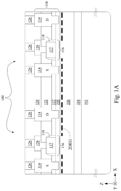
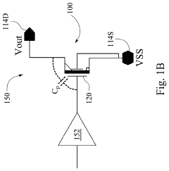
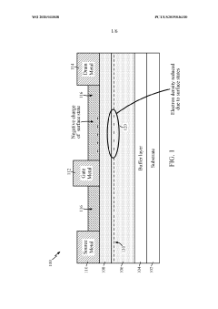
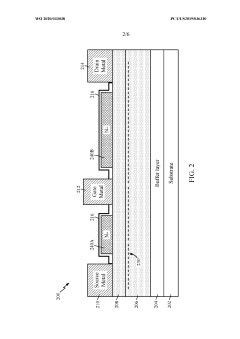
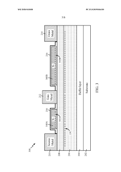
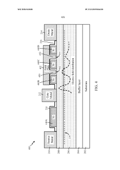
Gallium nitride high electron mobility transistor
PatentPendingUS20230395694A1
Innovation
- The solution involves forming a second AlGaN layer with a different composition over the AlGaN-GaN heterojunction, using sidewall spacers and selective epitaxy to decouple on-resistance from the threshold voltage, achieved by increasing the aluminum concentration in the AlGaN layer and adjusting its thickness, thereby enhancing spontaneous and piezoelectric polarization effects.
Gallium nitride high electron mobility transistor with ledges and field plates
PatentWO2020033038A1
Innovation
- Incorporating n-doped protuberances, or ledges, between the gate and source/drain electrodes, and optionally using field plates, to reduce surface states and increase channel electron density, thereby enhancing breakdown voltage and switching efficiency.
Supply Chain Analysis for GaN HEMT Production
The GaN HEMT supply chain represents a complex ecosystem involving raw materials, substrate manufacturing, epitaxial growth, device fabrication, packaging, and testing. Silicon carbide (SiC) remains the dominant substrate material for GaN HEMT production, accounting for approximately 85% of the market, while sapphire and silicon substrates serve specific application niches. The geographical distribution of this supply chain shows significant concentration, with the United States, Japan, and Europe controlling approximately 70% of high-quality substrate production capacity.
Raw material sourcing presents a notable vulnerability in the GaN HEMT supply chain. Gallium, a critical element for GaN epitaxial layers, faces supply constraints with China controlling over 95% of global production. This concentration creates potential bottlenecks and geopolitical risks that manufacturers must navigate through diversification strategies and recycling initiatives.
Epitaxial growth represents another critical bottleneck in the production process, requiring specialized equipment and expertise. Metal-Organic Chemical Vapor Deposition (MOCVD) systems, essential for high-quality GaN epitaxial layers, are primarily supplied by only three major manufacturers: Aixtron (Germany), Veeco (USA), and AMEC (China). This limited supplier base creates potential constraints as demand increases.
The fabrication segment shows greater diversity with foundry services offered by companies including WIN Semiconductors, Global Foundries, and TSMC. However, specialized GaN process capabilities remain concentrated among a smaller subset of these providers, creating potential capacity limitations as market adoption accelerates.
Packaging and testing infrastructure for GaN HEMTs has evolved from traditional silicon-based approaches, with specialized solutions now addressing the unique thermal and electrical characteristics of GaN devices. This segment has seen significant investment from companies like Amkor, ASE Group, and Carsem to develop GaN-specific packaging solutions.
Vertical integration strategies are increasingly evident among major players like Infineon, STMicroelectronics, and Wolfspeed, who are securing their supply chains through strategic acquisitions and partnerships. This trend reflects the strategic importance of GaN HEMT technology and concerns about supply chain resilience.
The COVID-19 pandemic exposed vulnerabilities in the GaN HEMT supply chain, prompting increased regionalization efforts. Major markets including the US, EU, and Japan have initiated programs to strengthen domestic semiconductor capabilities, including GaN technology, through substantial funding initiatives and policy support.
Regulatory Framework Impacting GaN HEMT Adoption
The regulatory landscape surrounding GaN HEMT technology has evolved significantly in recent years, creating both opportunities and challenges for market adoption. Government policies across major economies have increasingly recognized the strategic importance of wide bandgap semiconductors, including GaN, leading to supportive frameworks that accelerate commercialization. In the United States, the CHIPS Act has allocated substantial funding for semiconductor research and manufacturing, with specific provisions benefiting GaN technology development. Similarly, the European Union's Important Projects of Common European Interest (IPCEI) on Microelectronics has designated GaN as a critical technology deserving of targeted investment and regulatory support.
Environmental regulations have also shaped the GaN HEMT market trajectory. The global push toward energy efficiency has resulted in stringent power consumption standards for electronic devices, indirectly favoring GaN HEMTs due to their superior efficiency compared to silicon alternatives. For instance, the European Ecodesign Directive has established increasingly demanding efficiency requirements for power supplies and electronic systems, creating regulatory tailwinds for GaN adoption in consumer electronics and industrial applications.
Military and defense applications face particularly complex regulatory considerations. Export controls, including the U.S. International Traffic in Arms Regulations (ITAR) and Export Administration Regulations (EAR), impose significant compliance requirements on GaN HEMT manufacturers serving defense markets. These regulations have influenced supply chain structures and international collaboration patterns, sometimes limiting technology transfer but also creating protected market segments for domestic producers.
Telecommunications standards and regulations have emerged as another critical factor affecting GaN HEMT adoption. As 5G infrastructure deployment accelerates globally, regulatory bodies like the Federal Communications Commission (FCC) and the International Telecommunication Union (ITU) have established technical specifications that increasingly favor GaN-based power amplifiers due to their efficiency at higher frequencies. These standards effectively mandate performance levels that are challenging to achieve without GaN technology.
Safety certification requirements present additional regulatory hurdles. GaN HEMT devices must undergo rigorous testing to meet standards such as UL, CE, and various industry-specific certifications before commercial deployment. The relative newness of GaN technology has sometimes resulted in certification processes that were initially designed for silicon devices, requiring adaptation and occasionally causing delays in product launches.
Intellectual property regulations have also significantly impacted the GaN HEMT landscape. Patent protection strategies vary across regions, with different approaches to licensing and cross-licensing agreements. The complex patent ecosystem surrounding GaN technology has led to strategic alliances and occasional litigation, influencing market structure and technology access.
Unlock deeper insights with Patsnap Eureka Quick Research — get a full tech report to explore trends and direct your research. Try now!
Generate Your Research Report Instantly with AI Agent
Supercharge your innovation with Patsnap Eureka AI Agent Platform!