How Do GaN HEMTs Improve Efficiency In Power Converters?
SEP 5, 202510 MIN READ
Generate Your Research Report Instantly with AI Agent
Patsnap Eureka helps you evaluate technical feasibility & market potential.
GaN HEMT Technology Background and Objectives
Gallium Nitride (GaN) High Electron Mobility Transistors (HEMTs) represent a revolutionary advancement in semiconductor technology that has been evolving since the early 1990s. Initially developed for RF applications in telecommunications and radar systems, GaN HEMTs have progressively expanded into power electronics due to their superior material properties compared to traditional silicon-based devices. The wide bandgap nature of GaN (3.4 eV versus 1.1 eV for silicon) enables these devices to withstand higher electric fields and operate at elevated temperatures, making them ideal candidates for high-efficiency power conversion applications.
The technological evolution of GaN HEMTs has been marked by significant milestones, including the development of enhancement-mode devices around 2010, which eliminated the need for negative gate drive voltages and simplified circuit design. Further advancements in epitaxial growth techniques, particularly Metal-Organic Chemical Vapor Deposition (MOCVD), have enabled the production of high-quality GaN layers on various substrates, including silicon, which has substantially reduced manufacturing costs.
Current technological trends in GaN HEMT development focus on increasing power density, improving thermal management, enhancing reliability, and reducing parasitic elements. The integration of GaN devices with advanced packaging technologies, such as embedded die packaging and chip-scale packaging, is enabling unprecedented levels of miniaturization and efficiency in power converter designs.
The primary objective of GaN HEMT technology in power converters is to achieve significantly higher efficiency than conventional silicon-based solutions. This is accomplished through reduced switching losses due to lower gate charge and output capacitance, as well as lower conduction losses resulting from the high electron mobility in the two-dimensional electron gas (2DEG) channel. These characteristics allow for operation at much higher switching frequencies (often exceeding 1 MHz), which enables the use of smaller passive components and results in more compact and lightweight power converter designs.
Additional technical goals include pushing the boundaries of power density beyond 50 W/cm³, achieving junction temperatures above 200°C for enhanced reliability in harsh environments, and developing innovative gate driver solutions that can fully exploit the switching speed capabilities of GaN HEMTs while ensuring safe operation. The ultimate aim is to enable a new generation of power converters with efficiency exceeding 99% across a wide load range, which would represent a paradigm shift in energy conservation for applications ranging from consumer electronics to electric vehicles and renewable energy systems.
The trajectory of GaN HEMT technology suggests continued improvements in device performance, reliability, and cost-effectiveness, potentially leading to widespread adoption across numerous power electronics applications where efficiency is paramount.
Market Demand Analysis for High-Efficiency Power Converters
The global power electronics market is experiencing unprecedented growth, driven by increasing demand for energy-efficient solutions across multiple sectors. The power converter segment specifically is projected to reach $29.1 billion by 2026, growing at a CAGR of 7.2% from 2021. This growth is primarily fueled by the urgent need for high-efficiency power conversion technologies that can minimize energy losses and reduce carbon footprints.
Industrial applications represent the largest market segment for high-efficiency power converters, accounting for approximately 35% of the total market share. Manufacturing facilities are increasingly adopting advanced power conversion systems to reduce operational costs and meet stringent energy efficiency regulations. The automotive sector follows closely, with electric vehicles (EVs) and hybrid electric vehicles (HEVs) creating substantial demand for compact, lightweight, and highly efficient power converters.
Consumer electronics constitutes another significant market segment, with manufacturers seeking power conversion solutions that enable longer battery life and faster charging capabilities. The telecommunications industry also demonstrates growing demand, particularly for efficient power supplies in data centers and network infrastructure, where even marginal improvements in efficiency translate to substantial energy savings at scale.
Geographically, Asia-Pacific leads the market with approximately 40% share, driven by rapid industrialization, expanding electronics manufacturing, and aggressive renewable energy adoption in countries like China, Japan, and South Korea. North America and Europe follow with 25% and 22% market shares respectively, where stringent energy efficiency regulations and sustainability initiatives are driving adoption.
The market is witnessing a clear shift toward wide-bandgap (WBG) semiconductor technologies, particularly GaN HEMTs, which offer superior performance compared to traditional silicon-based solutions. Industry surveys indicate that 78% of power electronics engineers are considering GaN for their next designs, highlighting the growing market acceptance of this technology.
Key market drivers include increasingly stringent energy efficiency regulations worldwide, rising electricity costs, growing renewable energy integration requiring efficient power conversion, and the miniaturization trend in electronics demanding higher power density solutions. The total addressable market for GaN-based power converters specifically is expected to grow from $1.1 billion in 2021 to $4.3 billion by 2026, representing one of the fastest-growing segments within power electronics.
Customer requirements are evolving toward solutions that not only offer higher efficiency but also provide higher switching frequencies, reduced form factors, and improved thermal performance – all areas where GaN HEMTs demonstrate significant advantages over conventional technologies.
Current Status and Challenges in GaN HEMT Implementation
The global GaN HEMT (Gallium Nitride High Electron Mobility Transistor) market has experienced significant growth in recent years, with adoption accelerating across multiple power conversion applications. Currently, commercial GaN HEMTs are available with voltage ratings primarily in the 100V to 650V range, with some manufacturers pushing toward 900V and beyond. These devices have demonstrated superior switching performance compared to traditional silicon MOSFETs, with switching frequencies reaching into the MHz range while maintaining high efficiency.
Despite promising advancements, GaN HEMT implementation faces several critical challenges. Thermal management remains a significant concern as the high power density of GaN devices creates localized hotspots that can degrade performance and reliability. Current packaging technologies often limit the full potential of GaN chips, with traditional wire bonding introducing parasitic inductances that compromise high-frequency operation. More advanced packaging solutions like embedded die technology are emerging but remain costly.
Reliability concerns persist in the industry, particularly regarding dynamic RDS(on) degradation under high-voltage switching conditions. This phenomenon, where on-resistance increases over time, can reduce efficiency gains and create uncertainty about long-term performance. Additionally, gate driving presents unique challenges due to GaN HEMTs' lower gate threshold voltages and sensitivity to overvoltage conditions, requiring specialized gate driver ICs with precise voltage control.
The cost factor remains a significant barrier to widespread adoption. While prices have decreased substantially over the past decade, GaN solutions still command a premium of approximately 1.5-3x compared to silicon alternatives. This cost differential is particularly challenging for price-sensitive consumer applications, though the gap continues to narrow as production volumes increase.
Geographically, GaN HEMT development shows distinct regional characteristics. North America leads in innovation with companies like EPC, GaN Systems (now Infineon), and Navitas pioneering commercial applications. Asia, particularly Japan and China, has invested heavily in manufacturing infrastructure, with companies like Innoscience scaling production to drive costs down. Europe maintains strength in automotive and industrial applications, with STMicroelectronics and Infineon focusing on reliability and standardization.
Standardization and qualification frameworks represent another significant challenge. Unlike silicon devices with well-established reliability standards, GaN qualification procedures are still evolving. The industry is working toward consensus on testing methodologies specific to GaN's unique failure mechanisms, with organizations like JEDEC developing specialized standards for wide bandgap semiconductors.
Integration challenges persist at the system level, as optimal GaN implementation often requires redesigning power conversion topologies rather than simple component substitution. Engineers must reconsider PCB layouts, magnetic components, and control strategies to fully leverage GaN's high-speed switching capabilities.
Current GaN HEMT Solutions for Power Conversion
01 Device structure optimization for improved efficiency
Various structural modifications in GaN HEMTs can significantly enhance their efficiency. These include optimized gate designs, improved channel structures, and novel buffer layer configurations. By carefully engineering the device architecture, power losses can be reduced while maintaining high switching speeds. Advanced epitaxial growth techniques and substrate selection also play crucial roles in minimizing defects and improving thermal management, which directly impacts device efficiency.- Device structure optimization for improved efficiency: Various structural modifications in GaN HEMTs can significantly enhance their efficiency. These include optimized gate designs, improved channel structures, and novel buffer layer configurations. By carefully engineering the device architecture, power losses can be reduced while maintaining high electron mobility in the channel. These structural optimizations help in achieving higher breakdown voltages and better thermal management, which are crucial for high-efficiency operation.
- Advanced materials and fabrication techniques: The efficiency of GaN HEMTs can be enhanced through the use of advanced materials and fabrication techniques. This includes the development of high-quality epitaxial layers, improved ohmic contacts, and novel dielectric materials for passivation. Advanced fabrication processes such as selective area growth and precise etching techniques help in reducing parasitic elements and improving carrier transport properties, leading to higher efficiency devices.
- Thermal management solutions: Effective thermal management is critical for maintaining high efficiency in GaN HEMTs. Various approaches include the integration of heat sinks, thermal vias, and advanced packaging techniques. Improved thermal interfaces and substrate materials with higher thermal conductivity help in dissipating heat more efficiently. These solutions prevent performance degradation due to self-heating effects and extend the operational lifetime of the devices.
- Power conversion circuit design: The efficiency of GaN HEMT-based power systems can be optimized through innovative circuit designs. This includes resonant switching topologies, synchronous rectification techniques, and advanced gate driving methods. By minimizing switching losses and optimizing operating frequencies, these circuit designs leverage the inherent advantages of GaN HEMTs such as fast switching speeds and low on-resistance to achieve higher power conversion efficiencies.
- Reliability enhancement techniques: Various techniques can be employed to enhance the reliability and long-term efficiency of GaN HEMTs. These include surface passivation methods, edge termination designs, and field plate structures to manage electric fields. Stress testing and degradation mechanism studies help in developing robust devices that maintain their efficiency over extended operation. Additionally, compensation techniques for threshold voltage shifts and current collapse phenomena contribute to stable performance under various operating conditions.
02 Power management and thermal solutions
Effective power management and thermal solutions are essential for maximizing GaN HEMT efficiency. Innovations in heat dissipation techniques, including advanced packaging methods and thermal interface materials, help maintain optimal operating temperatures. Integration of power management circuits with GaN HEMTs enables dynamic control of operating parameters, reducing power consumption during different load conditions. These approaches collectively minimize energy losses and extend device lifetime under high-power operation.Expand Specific Solutions03 Material composition and doping techniques
The efficiency of GaN HEMTs is heavily influenced by material composition and doping strategies. Innovations in barrier layer materials, such as AlGaN/GaN heterostructures with optimized aluminum content, enhance carrier mobility and confinement. Advanced doping techniques, including selective area doping and graded doping profiles, help control threshold voltage and reduce parasitic resistances. Novel materials for ohmic contacts and passivation layers further contribute to reducing interface states and improving overall device performance.Expand Specific Solutions04 Circuit integration and application-specific designs
Integration of GaN HEMTs into specialized circuits and application-specific designs enhances system-level efficiency. Monolithic integration of multiple components, including drivers, protection circuits, and passive elements, reduces parasitic effects and improves switching performance. Custom designs for specific applications such as power converters, RF amplifiers, and motor drives leverage the unique properties of GaN HEMTs to achieve optimal efficiency. Advanced packaging techniques enable higher power density while maintaining thermal performance.Expand Specific Solutions05 Reliability enhancement techniques
Improving the reliability of GaN HEMTs directly impacts their long-term efficiency. Passivation techniques and surface treatments reduce current collapse and dynamic on-resistance, which are common efficiency-limiting factors. Field plate structures and edge termination designs help manage peak electric fields, preventing premature breakdown. Stress testing methodologies and lifetime prediction models enable the development of more robust devices that maintain high efficiency throughout their operational lifetime. Advanced characterization techniques help identify and mitigate degradation mechanisms.Expand Specific Solutions
Key Industry Players in GaN Power Electronics
The GaN HEMT power converter market is experiencing rapid growth, currently in the early mainstream adoption phase with a projected market size exceeding $2 billion by 2026. Technical maturity varies among key players: established semiconductor leaders like Wolfspeed, Texas Instruments, and Infineon Technologies Austria have advanced commercial solutions, while innovative specialists such as Transphorm, Cambridge GaN Devices, and InnoScience are driving next-generation developments. Academic institutions including Xidian University and University of Electronic Science & Technology of China contribute fundamental research. The competitive landscape features both vertically integrated manufacturers (Wolfspeed, ROHM) and fabless design companies (Power Integrations), with increasing competition from Asian manufacturers challenging traditional Western dominance in this transformative power electronics technology.
Wolfspeed, Inc.
Technical Solution: Wolfspeed has pioneered GaN HEMT technology for power conversion applications, focusing on silicon carbide (SiC) and GaN-on-SiC solutions. Their GaN HEMTs feature lateral device structures with high electron mobility channels formed at the AlGaN/GaN heterojunction interface. This design enables significantly faster switching speeds (up to 100x faster than silicon) and lower on-resistance, resulting in power converters with efficiency exceeding 98%. Wolfspeed's latest generation devices incorporate advanced field plate structures to manage peak electric fields, allowing operation at higher voltages (650V+) while maintaining reliability. Their proprietary passivation techniques minimize current collapse phenomena, ensuring consistent performance under high-frequency switching conditions. Wolfspeed has demonstrated GaN-based power converters achieving power densities of 3-4x higher than silicon equivalents while reducing switching losses by up to 80%.
Strengths: Industry-leading switching performance with minimal losses; extensive reliability testing and qualification; mature manufacturing processes with high yield rates. Weaknesses: Higher cost compared to silicon solutions; requires specialized gate drivers to fully utilize high-speed switching capabilities; thermal management challenges at highest power densities.
Texas Instruments Incorporated
Technical Solution: Texas Instruments has developed an integrated GaN HEMT solution that combines power stage, gate driver, and protection features in a single package. Their GaN technology utilizes an enhancement-mode architecture with proprietary gate structure that enables normally-off operation without requiring a cascode configuration. TI's GaN HEMTs feature ultra-low gate charge (Qg) and output capacitance (Coss), allowing switching frequencies up to 2MHz with minimal losses. This translates to power converter efficiency improvements of 3-5% compared to silicon solutions. Their devices incorporate advanced thermal management techniques, including flip-chip packaging that reduces thermal resistance by up to 30%. TI has demonstrated GaN-based power converters achieving power densities exceeding 100W/in³ in applications like server power supplies and industrial motor drives. Their integrated solution approach simplifies design complexity while providing built-in protection features like overcurrent, overvoltage, and thermal shutdown, addressing key reliability concerns in GaN implementation.
Strengths: Highly integrated solution reduces component count and design complexity; comprehensive protection features enhance system reliability; extensive design support ecosystem. Weaknesses: Limited voltage range compared to some competitors; higher cost than discrete solutions; proprietary architecture requires specific design approaches.
Critical Technical Analysis of GaN HEMT Architectures
Gallium nitride high electron mobility transistor
PatentPendingUS20230395694A1
Innovation
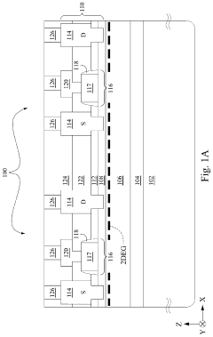
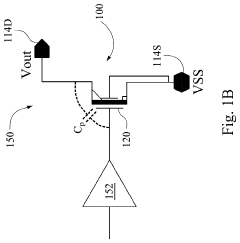
- The solution involves forming a second AlGaN layer with a different composition over the AlGaN-GaN heterojunction, using sidewall spacers and selective epitaxy to decouple on-resistance from the threshold voltage, achieved by increasing the aluminum concentration in the AlGaN layer and adjusting its thickness, thereby enhancing spontaneous and piezoelectric polarization effects.
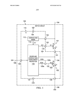
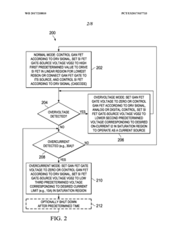
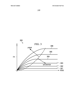
Overvoltage protection and short-circuit withstanding for gallium nitride devices
PatentWO2017218810A1
Innovation
- A driver and current source circuit are integrated with GaN transistors to detect overvoltage and overcurrent conditions, allowing controlled current sinking and cascode configuration to prevent damage, using a low voltage silicon transistor as a current source, either monolithically or in a dual-die configuration, to provide overvoltage and short-circuit protection.
Thermal Management Strategies for GaN Power Devices
Thermal management is a critical aspect of GaN HEMT implementation in power conversion systems. Due to their high power density and switching frequencies, GaN devices generate significant heat that must be effectively dissipated to maintain reliability and performance advantages. Conventional silicon-based cooling solutions often prove inadequate for GaN's thermal requirements, necessitating innovative approaches to thermal management.
The primary thermal challenge with GaN HEMTs stems from their concentrated heat generation in a small active region, creating localized hotspots that can reach temperatures exceeding 200°C during operation. This thermal concentration is exacerbated by GaN's lower thermal conductivity compared to silicon carbide alternatives, requiring more sophisticated cooling strategies to maintain junction temperatures within safe operating limits.
Advanced packaging technologies have emerged as a crucial element in GaN thermal management. Direct bonded copper (DBC) substrates and insulated metal substrates (IMS) provide superior thermal pathways compared to traditional FR4 PCB materials. Novel approaches such as double-sided cooling, where heat is extracted from both top and bottom surfaces of the device, have demonstrated up to 30% improvement in thermal resistance compared to single-sided solutions.
Active cooling techniques including liquid cooling systems and microfluidic channels integrated directly into GaN packages represent the cutting edge of thermal management. These solutions can achieve thermal resistances below 0.1°C/W, enabling GaN devices to operate at their full power density potential without thermal limitations. However, these approaches introduce additional complexity, cost, and reliability considerations that must be balanced against performance benefits.
Thermal interface materials (TIMs) play a vital role in the thermal stack, with next-generation materials such as phase-change metals, graphene-enhanced compounds, and liquid metal TIMs offering thermal conductivities exceeding 20 W/m·K. These advanced materials minimize the thermal boundary resistance between the GaN device and heat dissipation structures, addressing a critical bottleneck in the thermal pathway.
System-level thermal design considerations are equally important, with optimized PCB layouts featuring thermal vias, copper coins, and strategic component placement to facilitate heat spreading. Computational fluid dynamics (CFD) modeling has become an essential tool for predicting thermal behavior and optimizing cooling solutions before physical prototyping, reducing development cycles and ensuring thermal requirements are met under all operating conditions.
The integration of temperature sensors and dynamic thermal management algorithms enables real-time monitoring and adaptive control of GaN power systems, preventing thermal runaway while maximizing performance. These intelligent thermal management approaches represent a paradigm shift from static cooling solutions to dynamic systems that respond to changing thermal loads and environmental conditions.
Cost-Performance Trade-offs in GaN HEMT Adoption
The adoption of GaN HEMTs in power conversion applications presents significant cost-performance trade-offs that organizations must carefully evaluate. While GaN technology offers superior efficiency and performance characteristics, its implementation involves higher initial costs compared to traditional silicon-based solutions. The current price premium for GaN devices ranges from 1.5 to 3 times that of equivalent silicon MOSFETs, depending on voltage rating and production volume.
This cost differential stems primarily from manufacturing complexities, lower production volumes, and the relatively nascent state of GaN fabrication infrastructure. However, a comprehensive total cost of ownership (TCO) analysis reveals more nuanced considerations beyond component pricing. The enhanced efficiency of GaN-based converters translates to reduced cooling requirements, smaller passive components, and more compact designs, potentially offsetting the higher semiconductor costs through system-level savings.
Performance advantages must be quantified against cost implications across different application scenarios. In high-frequency applications operating above 500 kHz, GaN HEMTs demonstrate clear advantages with efficiency improvements of 2-5% over silicon alternatives. This efficiency gain becomes particularly valuable in data centers and telecommunications infrastructure, where the lifetime energy savings can justify the higher initial investment with ROI periods of 1-3 years.
For consumer electronics and automotive applications, the value proposition varies significantly based on power levels and operating conditions. Mid-power applications (500W-3kW) typically represent the current "sweet spot" where GaN benefits are maximized relative to cost premiums. Below this range, the absolute efficiency gains may not justify the cost difference, while above it, silicon carbide (SiC) devices may offer more competitive performance-cost ratios.
Manufacturing scale remains a critical factor in the cost equation. Industry projections suggest GaN device costs will decrease by approximately 10-15% annually as production volumes increase and manufacturing processes mature. This trend is accelerating as major semiconductor manufacturers expand their GaN production capabilities, with several foundries announcing capacity expansions specifically for wide-bandgap semiconductors.
Design complexity presents another important consideration in the cost-performance balance. GaN HEMTs require more sophisticated gate drivers, careful PCB layout, and enhanced EMI mitigation strategies. These design requirements can increase engineering costs and development time, particularly for organizations with limited experience in high-frequency power electronics design. However, the growing availability of reference designs, evaluation boards, and application notes from semiconductor manufacturers is gradually reducing these barriers to adoption.
Unlock deeper insights with Patsnap Eureka Quick Research — get a full tech report to explore trends and direct your research. Try now!
Generate Your Research Report Instantly with AI Agent
Supercharge your innovation with Patsnap Eureka AI Agent Platform!