

How Do GaN HEMTs Enable High-Frequency Power Conversion?
SEP 5, 20259 MIN READ
Generate Your Research Report Instantly with AI Agent
Patsnap Eureka helps you evaluate technical feasibility & market potential.
GaN HEMT Technology Background and Objectives
Gallium Nitride High Electron Mobility Transistors (GaN HEMTs) represent a revolutionary advancement in semiconductor technology that has evolved significantly over the past three decades. Initially developed for defense and aerospace applications in the 1990s, GaN technology has progressively transitioned into commercial power electronics, marking a paradigm shift from traditional silicon-based devices. The wide bandgap properties of GaN (3.4 eV compared to silicon's 1.1 eV) enable these devices to operate at substantially higher voltages, frequencies, and temperatures than conventional silicon transistors.
The evolution of GaN HEMTs has been characterized by continuous improvements in material quality, device architecture, and manufacturing processes. Early challenges included high defect densities in GaN epitaxial layers and reliability concerns, which have been systematically addressed through innovations in substrate technology and epitaxial growth techniques. The transition from silicon carbide to silicon substrates for GaN epitaxy represented a critical milestone, significantly reducing production costs while maintaining performance advantages.
Current technical objectives for GaN HEMT development focus on several key areas: increasing power density to exceed 5 kW/cm³, improving switching frequencies beyond 10 MHz, enhancing thermal management capabilities, and reducing manufacturing costs to achieve price parity with silicon devices in mainstream applications. Additionally, researchers aim to extend operating voltages beyond 1200V for medium-voltage applications while simultaneously improving device reliability and operational lifetime.
The technology trajectory indicates a clear trend toward monolithic integration, where multiple GaN power devices and control circuitry are fabricated on a single chip. This integration promises to further enhance switching performance by minimizing parasitic inductances and capacitances that limit high-frequency operation. Concurrently, efforts are underway to develop normally-off (enhancement-mode) GaN HEMTs that offer improved safety and simplified gate drive requirements compared to their normally-on counterparts.
From a global perspective, GaN HEMT technology has emerged as a strategic focus area for major economies, with significant research investments in North America, Europe, and East Asia. The technology is positioned to enable critical advancements in power electronics for electric vehicles, renewable energy systems, data centers, and telecommunications infrastructure, aligning with global initiatives for energy efficiency and carbon reduction. The ultimate goal is to establish GaN HEMTs as the dominant technology for high-frequency power conversion applications where efficiency, power density, and thermal performance are paramount considerations.
Market Demand for High-Frequency Power Conversion
The global market for high-frequency power conversion technologies has experienced substantial growth in recent years, driven primarily by increasing demands for more efficient, compact, and high-performance power electronics systems. This market expansion is particularly evident in sectors such as telecommunications, data centers, renewable energy, automotive, and consumer electronics, where power density and efficiency are critical competitive factors.
In the telecommunications sector, the rollout of 5G infrastructure has created significant demand for high-frequency power conversion solutions. Base stations require compact, efficient power supplies capable of operating at higher frequencies to support increased data throughput while minimizing energy consumption and physical footprint. Industry analysts project the 5G infrastructure market to grow at a CAGR of over 30% through 2026, directly driving demand for advanced power conversion technologies.
Data centers represent another major market driver, with global data center power consumption reaching approximately 200 TWh annually. As these facilities face mounting pressure to reduce energy costs and carbon footprints, the adoption of high-efficiency power conversion technologies has become imperative. High-frequency operation enables smaller passive components, reducing overall system size while improving thermal performance—critical factors in dense computing environments.
The electric vehicle (EV) market presents perhaps the most dynamic growth opportunity for high-frequency power conversion. On-board chargers, DC-DC converters, and traction inverters all benefit from the size, weight, and efficiency advantages of high-frequency operation. With global EV sales growing by over 40% annually, automotive manufacturers are increasingly prioritizing power electronics that maximize range and minimize charging times.
Consumer electronics manufacturers continue to push for smaller, lighter devices with longer battery life, creating steady demand for miniaturized power conversion solutions. The ability to operate efficiently at high frequencies directly translates to smaller form factors and reduced heat generation—both essential for modern portable devices.
Industrial applications and renewable energy systems also contribute significantly to market growth. Solar inverters, wind power converters, and industrial motor drives all benefit from high-frequency operation, with the global renewable energy inverter market alone expected to reach $30 billion by 2027.
This market landscape has created intense competition among semiconductor technologies, with traditional silicon-based solutions increasingly challenged by wide-bandgap alternatives. End users across all sectors consistently prioritize three key performance metrics: efficiency (to reduce operating costs and thermal management requirements), power density (to minimize physical footprint), and reliability (to ensure consistent operation in demanding environments).
Current State and Challenges in GaN HEMT Development
Gallium Nitride High Electron Mobility Transistors (GaN HEMTs) have emerged as revolutionary components in power electronics, particularly for high-frequency applications. Currently, GaN HEMT technology has reached commercial maturity in several sectors, with devices operating at breakdown voltages ranging from 100V to 900V and frequencies up to several gigahertz. The global market has witnessed significant growth, with major semiconductor manufacturers including Infineon, Texas Instruments, GaN Systems, and Transphorm establishing strong production capabilities.
Despite impressive advancements, GaN HEMT technology faces several critical challenges. Reliability remains a primary concern, particularly regarding dynamic Ron effects and threshold voltage instability under high-temperature, high-voltage operations. These issues stem from electron trapping phenomena at the AlGaN/GaN interface and within the buffer layers, which can significantly degrade device performance over time.
Manufacturing scalability presents another substantial hurdle. While 6-inch and 8-inch GaN-on-Si wafers have become standard, the transition to larger wafer sizes faces challenges related to wafer bow, crystal defects, and thermal mismatch between GaN and silicon substrates. These issues directly impact yield rates and manufacturing costs, limiting broader market adoption.
Thermal management represents a persistent technical challenge. GaN HEMTs generate significant heat during high-frequency, high-power operation, and current packaging technologies struggle to efficiently dissipate this thermal energy. Advanced thermal interface materials and innovative package designs are under development but have not yet reached optimal performance levels for the most demanding applications.
The geographic distribution of GaN HEMT technology development shows concentration in North America, Europe, Japan, and increasingly China. The United States maintains leadership in military and aerospace applications, while Japan and Europe focus on automotive and industrial implementations. China has made substantial investments to reduce dependency on foreign technology, establishing several GaN semiconductor fabrication facilities in recent years.
Cost remains a significant barrier to widespread adoption. Despite improvements in manufacturing processes, GaN HEMTs still command a premium price compared to silicon alternatives. This cost differential, while narrowing, continues to limit penetration in price-sensitive consumer electronics markets.
Standardization issues further complicate industry growth, as different manufacturers employ varying approaches to device design, packaging, and characterization. This fragmentation creates challenges for system designers seeking to incorporate GaN technology into new products, particularly regarding reliability assessment and qualification procedures.
Current GaN HEMT Power Conversion Solutions
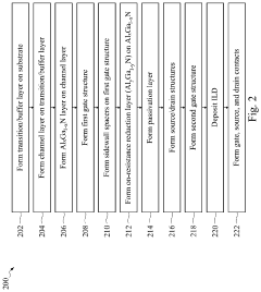
01 GaN HEMT device structure optimization for high-frequency applications
Optimizing the structure of GaN HEMT devices is crucial for high-frequency power conversion applications. This includes engineering the epitaxial layers, gate design, and channel configurations to enhance electron mobility and reduce parasitic capacitances. Advanced gate structures such as recessed gates, field plates, and optimized barrier layers help improve frequency response while maintaining high breakdown voltage capabilities necessary for power conversion.- Device structure optimization for GaN HEMTs: Optimizing the device structure of GaN HEMTs is crucial for high-frequency power conversion applications. This includes engineering the gate structure, channel design, and substrate materials to enhance electron mobility and reduce parasitic effects. Advanced structures such as recessed gates, field plates, and optimized barrier layers can significantly improve the high-frequency performance and power handling capabilities of these transistors.
- Thermal management techniques for GaN power devices: Effective thermal management is essential for GaN HEMTs operating at high frequencies and power levels. Various approaches include advanced packaging solutions, integration of heat spreaders, optimized die attachment methods, and substrate engineering. These techniques help dissipate heat efficiently, preventing thermal runaway and ensuring reliable operation under high-power conditions, which is critical for maintaining performance in power conversion applications.
- Gate driver and control circuit designs: Specialized gate driver and control circuit designs are necessary to fully leverage GaN HEMTs' high-frequency capabilities in power conversion. These circuits must handle fast switching speeds, minimize parasitic inductances, and provide precise timing control. Advanced gate driver topologies with optimized dead-time management and protection features enable efficient operation while preventing device failure due to voltage spikes or current overshoots during high-frequency switching.
- Power conversion topologies utilizing GaN HEMTs: Novel power conversion topologies specifically designed for GaN HEMTs can maximize the benefits of these devices in high-frequency applications. These include resonant and soft-switching converters, multilevel inverters, and hybrid topologies that reduce switching losses and electromagnetic interference. Such specialized circuit configurations enable higher power density, improved efficiency, and better thermal performance compared to conventional silicon-based designs.
- Material and fabrication innovations: Advancements in material science and fabrication techniques are enhancing GaN HEMT performance for high-frequency power conversion. These innovations include improved epitaxial growth methods, novel buffer layer designs, surface passivation techniques, and integration of complementary materials. Enhanced fabrication processes reduce defect densities and improve uniformity, resulting in devices with higher breakdown voltage, lower on-resistance, and better reliability under high-frequency switching conditions.
02 Thermal management solutions for GaN HEMT power converters
Effective thermal management is essential for GaN HEMT-based high-frequency power conversion systems. Various approaches include advanced packaging techniques, integration of heat dissipation structures, and substrate material selection to optimize thermal conductivity. These solutions help maintain device performance and reliability under high-power operation conditions by preventing performance degradation and extending device lifetime through efficient heat removal.Expand Specific Solutions03 GaN HEMT power conversion circuit topologies
Novel circuit topologies specifically designed for GaN HEMT-based power converters leverage the high-frequency capabilities of these devices. These include resonant converters, multilevel converter architectures, and soft-switching techniques that minimize switching losses. The circuit designs accommodate the fast switching speeds of GaN HEMTs while addressing challenges related to gate driving, parasitic inductances, and electromagnetic interference at high frequencies.Expand Specific Solutions04 GaN HEMT reliability enhancement techniques
Improving the reliability of GaN HEMTs for high-frequency power conversion involves addressing specific failure mechanisms such as current collapse, dynamic on-resistance, and gate leakage. Techniques include surface passivation, field plate optimization, buffer layer design, and specialized dielectric materials. These approaches help maintain stable performance under high-voltage switching conditions and extend the operational lifetime of devices in power conversion applications.Expand Specific Solutions05 Integration and packaging solutions for GaN HEMT power modules
Advanced integration and packaging technologies for GaN HEMT power modules focus on minimizing parasitic elements and improving thermal performance. These include system-in-package approaches, embedded die technologies, and co-packaging with gate drivers and passive components. Such integration solutions enable compact power conversion modules that maximize the high-frequency performance benefits of GaN HEMTs while addressing electromagnetic interference challenges.Expand Specific Solutions
Key Players in GaN Semiconductor Industry
The GaN HEMT power conversion market is in a growth phase, with increasing adoption across high-frequency applications due to superior switching performance compared to silicon. The market is expanding rapidly, projected to reach several billion dollars by 2026 with a CAGR exceeding 20%. Technologically, companies like Wolfspeed, Innoscience, and GaN Systems lead in commercialization, while established semiconductor players including Texas Instruments, QUALCOMM, and Huawei are investing heavily in GaN development. Research institutions such as Xidian University and University of Electronic Science & Technology of China are advancing fundamental technologies. The ecosystem shows varying maturity levels, with some companies offering production-ready devices while others focus on next-generation innovations to address thermal management and reliability challenges.
Wolfspeed, Inc.
Technical Solution: Wolfspeed has pioneered GaN HEMT technology for high-frequency power conversion through their proprietary HD-GaN (High Density GaN) platform. Their approach utilizes a lateral device structure with optimized gate design that enables switching frequencies exceeding 100 MHz while maintaining high power density. Wolfspeed's GaN HEMTs feature a unique epitaxial layer structure grown on SiC substrates, providing superior thermal conductivity (>3.5 W/cm·K) compared to traditional silicon-based devices. Their latest generation devices achieve on-resistance values below 40 mΩ and can operate at junction temperatures up to 175°C with minimal performance degradation. The company has developed specialized packaging solutions that minimize parasitic inductances to fully leverage GaN's high-speed switching capabilities, enabling power conversion efficiencies exceeding 98% in MHz-range operation.
Strengths: Industry-leading thermal performance due to SiC substrate integration; extremely high switching speeds enabling compact power system designs; mature manufacturing process with proven reliability. Weaknesses: Higher cost compared to silicon-based alternatives; requires specialized gate drivers to fully utilize switching capabilities; more complex thermal management requirements.
Power Integrations, Inc.
Technical Solution: Power Integrations has developed an innovative approach to GaN HEMT technology for high-frequency power conversion through their InnoSwitch™-GaN platform. Their solution integrates GaN HEMTs with advanced control circuitry in a single package, enabling simplified designs with reduced component count. Power Integrations' GaN technology utilizes a proprietary high-voltage GaN-on-Si process that achieves breakdown voltages exceeding 750V while maintaining low on-resistance (typically 170mΩ for 750V devices). Their integrated approach addresses one of the key challenges in GaN implementation - the interface between the high-speed GaN switch and its control circuitry. By incorporating specialized gate drivers optimized for GaN switching characteristics, their devices can operate efficiently at frequencies up to 1MHz. This enables power supply designs with power densities exceeding 30W/in³, significantly higher than conventional silicon-based solutions operating at 65-100kHz.
Strengths: Highly integrated solution reducing design complexity and time-to-market; robust protection features including thermal shutdown and overcurrent protection; simplified regulatory compliance through integrated safety features. Weaknesses: Less flexibility for custom designs compared to discrete solutions; limited to specific power ranges and topologies; higher cost per watt for very high-power applications compared to discrete implementations.
Core Innovations in GaN HEMT Device Physics
High-voltage GAN high electron mobility transistors
PatentWO2017181121A2
Innovation
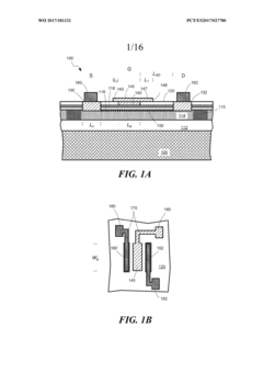
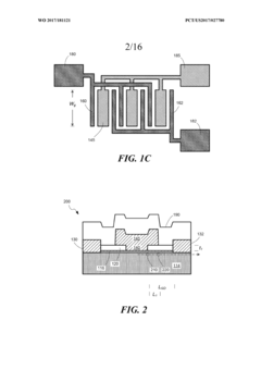
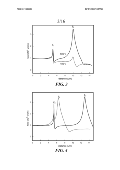
- The development of high-voltage HEMTs with a gallium-nitride material structure, including a buffer layer, conduction layer, barrier layer, gate, source, and drain, with a gate-connected field plate extending beyond the gate edges, and a thin gallium-oxide layer formed through oxygen plasma treatment, to enhance reverse-bias voltage withstand and reduce leakage currents.

Gallium nitride high electron mobility transistor
PatentPendingUS20230395694A1
Innovation
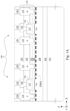
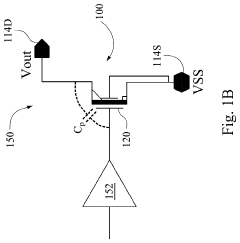
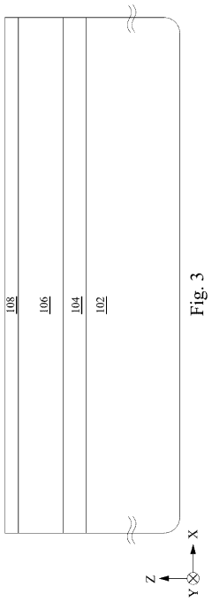
- The solution involves forming a second AlGaN layer with a different composition over the AlGaN-GaN heterojunction, using sidewall spacers and selective epitaxy to decouple on-resistance from the threshold voltage, achieved by increasing the aluminum concentration in the AlGaN layer and adjusting its thickness, thereby enhancing spontaneous and piezoelectric polarization effects.
Thermal Management Strategies for GaN HEMTs
Thermal management is a critical aspect of GaN HEMT technology that directly impacts the performance and reliability of high-frequency power conversion systems. The superior thermal conductivity of GaN (approximately 130 W/m·K) compared to silicon (148 W/m·K) provides a foundation for effective heat dissipation, but the high power density of GaN HEMTs presents significant thermal challenges that require innovative solutions.
Advanced substrate materials play a crucial role in thermal management strategies. Silicon carbide (SiC) substrates, with thermal conductivity of approximately 370-490 W/m·K, have become the preferred choice for high-power GaN applications, offering superior heat dissipation compared to traditional silicon or sapphire substrates. Diamond substrates, though still in development stages, promise even better thermal performance with conductivity exceeding 2000 W/m·K.
Package-level thermal solutions have evolved significantly to address GaN HEMT thermal requirements. Flip-chip packaging techniques eliminate wire bonds and provide direct thermal paths to heat sinks, reducing thermal resistance by up to 30% compared to conventional packages. Advanced thermal interface materials (TIMs) with enhanced thermal conductivity further optimize heat transfer between the device and cooling system.
Active cooling technologies are increasingly being integrated into GaN HEMT systems. Microfluidic cooling channels embedded directly into device packages can achieve thermal resistances below 0.1°C/W, enabling power densities exceeding 1 kW/cm². Two-phase cooling systems utilizing the latent heat of vaporization offer even greater cooling capacity for extreme power density applications.
Thermal simulation and modeling have become essential tools in GaN HEMT design. Finite element analysis (FEA) and computational fluid dynamics (CFD) enable accurate prediction of thermal hotspots and optimization of cooling strategies before physical prototyping. These simulation approaches have reduced thermal design cycles by approximately 40% while improving thermal performance.
Emerging thermal management approaches include heterogeneous integration of cooling elements directly within the semiconductor structure. Techniques such as through-substrate vias (TSVs) filled with high thermal conductivity materials create vertical thermal pathways that can reduce junction-to-case thermal resistance by up to 50%. Additionally, novel nanostructured materials like graphene-based thermal interface materials show promise for next-generation thermal solutions with thermal conductivities potentially exceeding 5000 W/m·K.
The implementation of effective thermal management strategies has enabled GaN HEMTs to achieve switching frequencies above 100 MHz while maintaining junction temperatures below critical thresholds, directly contributing to the technology's success in high-frequency power conversion applications.
Reliability and Qualification Standards for GaN Devices
The reliability and qualification of GaN HEMTs represent critical considerations for their widespread adoption in high-frequency power conversion applications. Unlike silicon-based devices with decades of established standards, GaN technology requires specialized qualification frameworks that address its unique material properties and failure mechanisms.
Industry standards organizations including JEDEC, AEC, and IEC have developed specific test protocols for GaN devices. JEDEC JEP180 and AEC-Q101 qualification standards have been adapted to address GaN-specific reliability concerns, with particular focus on dynamic RDS(on) degradation, threshold voltage instability, and gate leakage current—phenomena not typically problematic in silicon devices.
Accelerated life testing methodologies for GaN HEMTs include high-temperature reverse bias (HTRB), high-temperature gate bias (HTGB), and temperature-humidity-bias (THB) tests. These tests evaluate device performance under extreme conditions to predict long-term reliability. Additionally, power cycling and thermal cycling tests assess the robustness of GaN devices under repetitive thermal stress conditions typical in power conversion applications.
Time-dependent dielectric breakdown (TDDB) testing has emerged as particularly important for GaN technology due to the high electric fields present in these devices. Manufacturers typically guarantee minimum lifetimes of 10-15 years under rated operating conditions based on these accelerated tests and subsequent statistical modeling.
Field reliability data is increasingly becoming available as GaN deployment expands. Current data indicates failure rates below 10 FIT (failures in time, per billion device-hours) for properly qualified devices, comparable to mature silicon technologies. However, application-specific reliability considerations remain crucial, particularly for automotive and industrial applications where operating environments are harsh.
Mission profile-based qualification has gained prominence, where testing conditions are tailored to match the specific application environment rather than using generic standards. This approach has proven particularly valuable for GaN devices in telecommunications infrastructure and automotive applications, where operating conditions vary significantly.
Manufacturers have established comprehensive qualification processes that often exceed standard requirements. Companies like GaN Systems, EPC, Transphorm, and Infineon publish detailed reliability reports demonstrating compliance with industry standards while highlighting application-specific reliability metrics relevant to high-frequency power conversion scenarios.
Unlock deeper insights with Patsnap Eureka Quick Research — get a full tech report to explore trends and direct your research. Try now!
Generate Your Research Report Instantly with AI Agent
Supercharge your innovation with Patsnap Eureka AI Agent Platform!