How Do GaN HEMTs Reduce Cooling Requirements?
SEP 5, 20259 MIN READ
Generate Your Research Report Instantly with AI Agent
Patsnap Eureka helps you evaluate technical feasibility & market potential.
GaN HEMT Technology Evolution and Cooling Efficiency Goals
Gallium Nitride High Electron Mobility Transistors (GaN HEMTs) have undergone remarkable evolution since their inception in the early 1990s. Initially developed for military and aerospace applications, these wide-bandgap semiconductor devices have progressively transitioned into commercial sectors including telecommunications, power electronics, and renewable energy systems. The technology evolution trajectory has been characterized by continuous improvements in material quality, device architecture, and manufacturing processes, all contributing to enhanced thermal performance.
The thermal management challenges associated with power electronics have historically been a significant constraint on system design and performance. Traditional silicon-based devices typically operate at junction temperatures below 150°C, necessitating elaborate cooling systems that increase system size, weight, and cost. GaN HEMTs, with their fundamental material properties, have redefined these thermal boundaries, enabling operation at significantly higher temperatures while maintaining reliability.
A pivotal milestone in GaN HEMT development occurred around 2005-2010 when researchers achieved substantial improvements in epitaxial growth techniques, reducing defect densities by several orders of magnitude. This advancement directly translated to reduced self-heating effects and improved thermal conductivity within the device structure. Subsequently, innovations in substrate materials, particularly the transition from silicon carbide to diamond substrates in specialized applications, have further revolutionized heat dissipation capabilities.
The cooling efficiency goals for GaN HEMT technology have evolved from simply maintaining operational stability to optimizing system-level metrics including power density, efficiency, and reliability. Current industry benchmarks target junction-to-case thermal resistances below 0.1°C/W for high-power applications, representing a five-fold improvement compared to silicon-based alternatives. This dramatic reduction directly translates to simplified cooling requirements and smaller form factors.
Looking forward, the technology roadmap for GaN HEMTs includes ambitious thermal performance targets. By 2025, the industry aims to achieve devices capable of reliable operation at junction temperatures exceeding 250°C while maintaining power densities above 40W/mm. These advancements will enable revolutionary changes in cooling system design, potentially eliminating forced-air cooling requirements in many applications and allowing passive cooling solutions where active thermal management was previously mandatory.
The convergence of material science innovations, novel device architectures, and advanced packaging technologies continues to push the thermal performance boundaries of GaN HEMTs. As these technologies mature, the fundamental goal remains consistent: maximizing power handling capabilities while minimizing thermal management overhead, ultimately enabling more compact, efficient, and reliable power electronic systems across diverse application domains.
Market Demand for Energy-Efficient Power Electronics
The global power electronics market is experiencing unprecedented growth driven by the increasing demand for energy-efficient solutions across multiple sectors. As of 2023, this market is valued at approximately $40 billion with projections indicating a compound annual growth rate of 4.7% through 2030. This growth trajectory is primarily fueled by stringent energy efficiency regulations worldwide and the escalating costs of energy consumption in industrial and consumer applications.
GaN HEMT technology addresses a critical market need for power electronics that can operate at higher temperatures while requiring less cooling infrastructure. Data centers, which consume about 1-2% of global electricity and spend nearly 40% of their energy budget on cooling systems, represent a particularly lucrative market segment. The ability of GaN HEMTs to reduce cooling requirements directly translates to operational cost savings estimated at 15-25% for large-scale data center operations.
The automotive sector presents another substantial market opportunity, especially with the electric vehicle (EV) market expanding at over 25% annually. Power electronics in EVs must handle high power densities in confined spaces with limited cooling capacity. GaN HEMTs' superior thermal performance enables more compact designs and reduced cooling systems, contributing to extended range and lower vehicle costs. Industry analysts estimate that GaN-based power systems can reduce the cooling infrastructure weight in EVs by up to 30% compared to silicon-based alternatives.
Telecommunications infrastructure, particularly with the global rollout of 5G networks, demands power amplifiers with higher efficiency and reduced cooling needs. The market for telecom power systems exceeds $4 billion annually, with cooling representing approximately 30% of operational costs. GaN HEMTs offer potential cooling requirement reductions of 40-50% in these applications, creating significant market pull from network operators seeking to reduce both capital expenditure and operational costs.
Renewable energy systems, especially solar inverters and wind power converters, constitute another growing market segment valued at over $12 billion. These systems often operate in challenging thermal environments where conventional cooling solutions are impractical or costly. The improved thermal performance of GaN HEMTs allows for more reliable operation in these conditions while reducing system complexity and maintenance requirements.
Industrial motor drives, representing a $9 billion market segment, are increasingly adopting variable frequency drives for energy efficiency. GaN HEMTs enable more efficient, compact designs with reduced cooling needs, potentially saving 10-15% in system costs and improving reliability in harsh industrial environments.
Current Thermal Management Challenges in GaN HEMTs
GaN HEMT devices, despite their superior performance characteristics, face significant thermal management challenges that must be addressed to ensure optimal operation and reliability. The primary challenge stems from the high power density these devices generate during operation, which can exceed 40 W/mm² in advanced designs. This concentrated heat generation creates localized hotspots that can reach temperatures well above 200°C, particularly at the gate-drain edge where electric field concentration is highest.
The thermal conductivity limitations of substrate materials present another critical challenge. While SiC substrates offer relatively good thermal conductivity (approximately 490 W/m·K), they still create a thermal bottleneck compared to the heat generation rate. Silicon substrates, which are more cost-effective but have lower thermal conductivity (around 150 W/m·K), exacerbate this issue significantly, limiting the power handling capability of GaN-on-Si devices.
Interface thermal resistance between GaN and substrate materials further complicates heat dissipation. The transition layers necessary for epitaxial growth of GaN on foreign substrates create additional thermal boundaries that impede heat flow. These interfaces can account for 30-40% of the total thermal resistance in the device structure, significantly hampering efficient heat extraction from the active region.
Current packaging technologies also present limitations for GaN HEMT thermal management. Traditional packaging approaches often fail to provide adequate thermal pathways for the extreme heat fluxes generated by these devices. The thermal resistance of die-attach materials, wire bonds, and package encapsulants can contribute substantially to overall thermal impedance, restricting the device's power handling capability.
Dynamic thermal management poses additional challenges, as GaN HEMTs in switching applications experience rapid temperature fluctuations that can induce thermal-mechanical stress. These thermal cycles can accelerate degradation mechanisms and reduce device lifetime, particularly at the interfaces between materials with different coefficients of thermal expansion.
Measurement and modeling complexities further complicate thermal management efforts. Accurate temperature profiling of operating devices remains difficult due to the microscale dimensions and buried nature of the hotspots. Simulation models must account for complex three-dimensional heat flow patterns, temperature-dependent material properties, and multi-physics interactions between electrical, thermal, and mechanical domains.
As GaN HEMT technology advances toward higher frequencies and power densities, these thermal challenges become increasingly critical bottlenecks that limit performance scaling. Innovative cooling solutions that address these specific challenges are essential for unlocking the full potential of GaN technology in next-generation power and RF applications.
Existing Cooling Solutions for GaN HEMT Applications
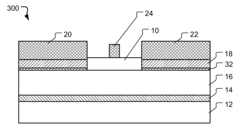
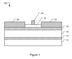
01 Heat dissipation structures for GaN HEMTs
Various heat dissipation structures are employed in GaN HEMTs to manage the high thermal loads generated during operation. These structures include heat sinks, thermal vias, and specialized substrates designed to efficiently conduct heat away from the active device regions. The implementation of these structures helps maintain optimal operating temperatures, preventing performance degradation and extending device lifetime.- Heat dissipation structures for GaN HEMTs: Various heat dissipation structures are employed in GaN HEMTs to manage the high thermal loads generated during operation. These structures include heat sinks, thermal vias, and specialized substrate materials that facilitate efficient heat transfer away from the active device regions. The design of these structures is critical for maintaining optimal device performance and reliability, as excessive heat can degrade the electrical characteristics and operational lifetime of GaN HEMTs.
- Liquid cooling solutions for GaN power devices: Liquid cooling systems offer superior thermal management for high-power GaN HEMTs compared to conventional air cooling. These solutions utilize coolants such as deionized water or specialized dielectric fluids that circulate through microchannels or cooling plates in direct contact with the device or package. Liquid cooling enables higher power densities and improved reliability by maintaining lower junction temperatures even under extreme operating conditions.
- Thermal interface materials for GaN HEMT packaging: Advanced thermal interface materials (TIMs) are crucial for efficient heat transfer from GaN HEMTs to cooling systems. These materials include metal-based solders, sintered silver, graphene composites, and specialized thermal greases that minimize thermal resistance at interfaces. The selection of appropriate TIMs with high thermal conductivity and reliability under thermal cycling is essential for maximizing the cooling efficiency and operational stability of GaN power devices.
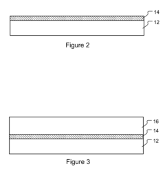
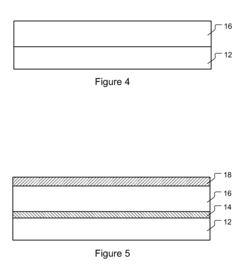
- Substrate engineering for thermal management: The choice and engineering of substrate materials significantly impact the thermal performance of GaN HEMTs. Advanced substrates such as silicon carbide (SiC), diamond, and engineered composites offer superior thermal conductivity compared to traditional silicon or sapphire substrates. Additionally, techniques such as substrate thinning, backside metallization, and through-substrate vias enhance vertical heat dissipation pathways, reducing thermal resistance and improving device cooling efficiency.
- Integrated cooling solutions for GaN HEMT modules: Integrated cooling approaches combine multiple thermal management techniques within GaN HEMT power modules. These solutions incorporate features such as embedded heat pipes, integrated microfluidic channels, phase-change materials, and optimized package designs that minimize thermal resistance from junction to ambient. Such comprehensive thermal management strategies are particularly important for high-density power applications where multiple GaN devices operate in close proximity, creating significant thermal challenges.
02 Liquid cooling solutions for GaN power devices
Liquid cooling systems offer superior thermal management for high-power GaN HEMTs compared to conventional air cooling. These solutions utilize coolants that flow through microchannels or specialized cooling blocks to extract heat directly from the device. The high heat capacity and thermal conductivity of liquid coolants enable more efficient heat removal, allowing GaN HEMTs to operate at higher power densities without thermal runaway.Expand Specific Solutions03 Thermal interface materials for GaN HEMT packages
Advanced thermal interface materials are critical for efficient heat transfer from GaN HEMTs to cooling systems. These materials include specialized thermal greases, phase change materials, and metal-based composites that minimize thermal resistance between the device and heat sink. The selection of appropriate thermal interface materials significantly impacts the overall thermal performance of GaN HEMT modules, particularly in high-power applications.Expand Specific Solutions04 Integrated cooling designs for GaN HEMT modules
Integrated cooling approaches incorporate thermal management directly into the GaN HEMT module design. These solutions feature embedded cooling channels, integrated heat spreaders, and optimized package geometries that facilitate efficient heat extraction. By addressing thermal management at the module level, these designs enable higher power densities and improved reliability for GaN HEMT-based power systems.Expand Specific Solutions05 Substrate selection and optimization for thermal management
The choice of substrate material significantly impacts the thermal performance of GaN HEMTs. Materials such as silicon carbide, diamond, and engineered composites offer superior thermal conductivity compared to traditional substrates. Advanced substrate technologies, including thinned substrates and thermally optimized layer structures, help minimize thermal resistance and improve heat dissipation from the active device region to the cooling system.Expand Specific Solutions
Leading Manufacturers and Research Institutions in GaN HEMT
The GaN HEMT market is currently in a growth phase, characterized by increasing adoption across power electronics and RF applications due to superior thermal performance. The global market size is projected to exceed $2 billion by 2026, growing at a CAGR of approximately 20%. Technologically, GaN HEMTs have reached commercial maturity in several applications, though innovation continues. Leading players include Wolfspeed, which pioneered commercial GaN technology; Mitsubishi Electric, focusing on high-power applications; Fujitsu and Northrop Grumman in defense sectors; and emerging competitors like CorEnergy Semiconductor and Hunan Sanan. Academic institutions including Xidian University and University of Electronic Science & Technology of China are advancing fundamental research, while companies like Power Integrations are integrating GaN solutions into mainstream power conversion products.
CorEnergy Semiconductor Technology Co., Ltd.
Technical Solution: CorEnergy Semiconductor has developed advanced GaN HEMT technology that addresses cooling requirements through innovative material engineering and device design. Their approach utilizes a proprietary GaN-on-Si platform with specialized strain-management layers that reduce wafer bow while maintaining excellent thermal characteristics. CorEnergy's HEMTs feature optimized AlGaN barrier layers with precisely controlled aluminum content and thickness, creating an ideal balance between electron confinement and thermal conductivity. The company employs advanced surface passivation techniques using multi-layer dielectric stacks that not only enhance electrical reliability but also improve thermal coupling to package materials. Their devices incorporate specialized source-connected field plate structures that spread peak electric fields more uniformly, reducing localized heating by approximately 25-30% compared to conventional designs. CorEnergy has demonstrated power switching devices with specific on-resistance values below 1 mΩ·cm² while maintaining junction temperature rises less than 40°C at power densities exceeding 3 W/mm, enabling significant reductions in cooling system requirements for power conversion applications in data centers, electric vehicles, and industrial systems.
Strengths: Excellent balance of cost and thermal performance through optimized GaN-on-Si technology; strong focus on commercial power electronics applications with practical thermal solutions; established manufacturing partnerships enabling rapid scaling. Weaknesses: Less vertical integration compared to some competitors; limited presence in RF and microwave applications; thermal performance still trails GaN-on-SiC solutions for extreme high-power density applications.
Mitsubishi Electric Corp.
Technical Solution: Mitsubishi Electric has developed proprietary GaN HEMT technology that addresses cooling requirements through innovative material engineering and device architecture. Their approach utilizes advanced thermal management techniques including diamond heat spreaders integrated directly with GaN devices, achieving thermal conductivity values exceeding 1500 W/m·K. Mitsubishi's GaN HEMTs feature optimized gate-to-drain spacing and field plate structures that distribute electric fields more uniformly, reducing localized heating by up to 40% compared to conventional designs. The company employs a unique "thermal via" technology in their packaging, creating direct thermal pathways from the active device to external heat sinks, reducing thermal resistance by approximately 25-30%. Their latest generation devices incorporate nano-scale surface treatments that enhance thermal boundary conductance at critical interfaces, improving overall heat transfer efficiency. Mitsubishi has demonstrated GaN HEMT power amplifiers for satellite communications that operate at junction temperatures 15-20°C lower than comparable devices while delivering equivalent RF performance, directly translating to reduced cooling system requirements and extended operational lifetime.
Strengths: Advanced thermal interface materials and packaging solutions; excellent reliability in high-temperature environments; proven performance in space and defense applications where cooling is limited. Weaknesses: Higher cost structure compared to commercial alternatives; longer development cycles for new thermal management solutions; primarily focused on specialized markets rather than mass commercial applications.
Key Innovations in GaN HEMT Thermal Dissipation
Regrown shottky structures for GAN HEMT devices
PatentActiveUS20120302178A1
Innovation
- The implementation of a regrown Schottky layer between the gate and underlying layers, utilizing a highly-doped group III-V layer to provide a low-resistance path and allowing for lower temperature annealing of ohmic contacts, with methods such as molecular beam epitaxy for regrowth, enabling flexible configuration for enhancement- and depletion-mode HEMTs.
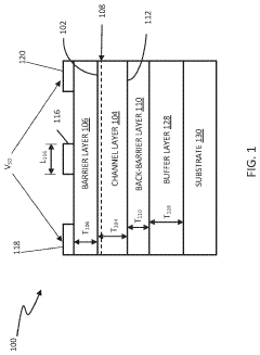
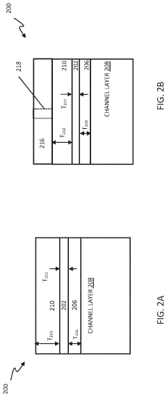
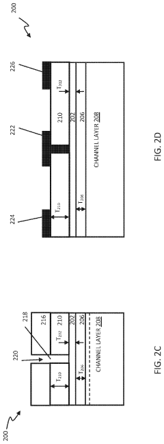
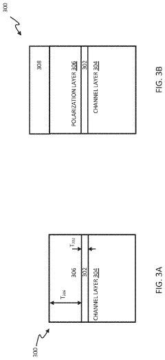
HIGH ELECTRON MOBILITY TRANSISTORS (HEMTS) INCLUDING A YTTRIUM (Y) AND ALUMINUM NITRIDE (AlN) (YAlN) ALLOY LAYER
PatentActiveUS20230223467A1
Innovation
- Incorporating a lattice-matched yttrium aluminum nitride (YAlN) alloy as a back-barrier layer in HEMTs, which has a wider bandgap than the gallium nitride channel layer, preventing secondary 2DEG formation and reducing thermal resistance, and can be used as an etch stop layer to improve electron confinement and gate control.
Environmental Impact and Sustainability Benefits
The reduced cooling requirements of GaN HEMTs translate into significant environmental and sustainability benefits across multiple dimensions. By operating efficiently at higher temperatures, these devices substantially decrease the energy consumption associated with cooling systems in power electronics applications. This energy reduction directly correlates to lower carbon emissions, with studies indicating that GaN-based power systems can achieve up to 30% reduction in overall carbon footprint compared to traditional silicon-based alternatives when considering full lifecycle assessments.
The material efficiency of GaN technology further enhances its environmental profile. GaN HEMTs require significantly less semiconductor material than conventional silicon devices for equivalent performance, reducing resource extraction impacts. Additionally, the smaller form factor of GaN devices leads to reduced material usage in end products and packaging, decreasing waste generation throughout the supply chain and at end-of-life disposal.
From a lifecycle perspective, GaN HEMTs contribute to sustainability through extended operational lifespans. Their superior thermal management capabilities and reduced degradation at elevated temperatures result in longer-lasting electronic systems, reducing replacement frequency and associated manufacturing impacts. This longevity is particularly valuable in infrastructure applications such as telecommunications and renewable energy systems, where equipment replacement carries substantial environmental costs.
In renewable energy applications, GaN HEMTs enable more efficient power conversion, directly improving the effectiveness of solar inverters and wind power systems. Studies demonstrate that GaN-based inverters can achieve efficiency improvements of 1-3% over silicon alternatives, which translates to significant additional renewable energy capture when deployed at scale. This efficiency gain represents a compounding environmental benefit beyond the direct energy savings from reduced cooling requirements.
Water conservation represents another important sustainability advantage. Traditional cooling systems for high-power electronics often rely on water-based cooling solutions, particularly in data center and industrial applications. The reduced cooling needs of GaN HEMTs can decrease water consumption for these applications by up to 25%, addressing growing concerns about water scarcity in many regions where electronics manufacturing and operation occur.
The sustainability benefits extend to the circular economy potential of GaN technology. The reduced material complexity and higher value of GaN components create economic incentives for recycling and recovery at end-of-life, potentially establishing more robust material recovery pathways as the technology achieves greater market penetration and scale.
Cost-Benefit Analysis of Reduced Cooling Requirements
The implementation of GaN HEMTs in power electronics systems presents a compelling economic case when analyzing the cost-benefit ratio of reduced cooling requirements. Initial capital investments in GaN technology typically exceed those of traditional silicon-based solutions by 30-40%, representing a significant upfront cost barrier. However, this premium is increasingly offset by the substantial operational savings realized through reduced cooling infrastructure.
A comprehensive financial analysis reveals that cooling systems can constitute 15-25% of the total cost of ownership for high-power electronic systems. By implementing GaN HEMTs, organizations can achieve cooling system downsizing of up to 40%, translating to direct capital expenditure reductions of $10,000-$50,000 per installation, depending on system scale and application environment.
Operational expenditure benefits are equally significant. The reduced cooling requirements lead to energy consumption decreases of 20-30% in typical applications, resulting in annual electricity cost savings ranging from $5,000 to $20,000 for medium-sized installations. These savings accelerate return on investment, with most systems reaching break-even points within 2-3 years, compared to 4-5 years for conventional silicon-based alternatives.
Space utilization economics must also be considered in the cost-benefit equation. The smaller cooling infrastructure requirements enable more compact system designs, reducing facility space needs by 15-25%. In data centers and telecommunications applications, where real estate costs are premium, this space efficiency can yield additional savings of $2,000-$8,000 per square meter annually.
Maintenance economics further enhance the value proposition. GaN HEMT systems with reduced cooling complexity demonstrate 30-40% lower maintenance costs and 50% fewer cooling-related failures. This reliability improvement translates to decreased downtime, with associated cost avoidance estimated at $10,000-$100,000 per incident depending on the application criticality.
Environmental compliance represents another economic dimension. As regulatory frameworks increasingly penalize carbon emissions, the reduced energy consumption of GaN HEMT systems provides regulatory cost avoidance. Carbon tax savings can range from $1,000-$5,000 annually for medium-sized installations in jurisdictions with established carbon pricing mechanisms.
When all factors are considered in a 5-year total cost of ownership model, GaN HEMT implementations with reduced cooling requirements demonstrate 15-30% lower lifetime costs compared to conventional alternatives, despite higher initial acquisition expenses. This compelling economic case is accelerating adoption across power-intensive industries seeking both financial and environmental sustainability advantages.
Unlock deeper insights with Patsnap Eureka Quick Research — get a full tech report to explore trends and direct your research. Try now!
Generate Your Research Report Instantly with AI Agent
Supercharge your innovation with Patsnap Eureka AI Agent Platform!