Impact Of Temperature On GaN HEMT Switching Performance
SEP 5, 20259 MIN READ
Generate Your Research Report Instantly with AI Agent
Patsnap Eureka helps you evaluate technical feasibility & market potential.
GaN HEMT Technology Background and Thermal Goals
Gallium Nitride High Electron Mobility Transistors (GaN HEMTs) have emerged as revolutionary power semiconductor devices over the past two decades, offering superior performance characteristics compared to traditional silicon-based technologies. The wide bandgap nature of GaN (3.4 eV compared to 1.1 eV for silicon) enables these devices to operate at higher voltages, frequencies, and power densities while maintaining efficiency. The development of GaN technology began in the 1990s primarily for RF applications in defense and telecommunications, but has since expanded significantly into power electronics applications.
The fundamental advantage of GaN HEMTs lies in their unique two-dimensional electron gas (2DEG) formation at the AlGaN/GaN heterojunction, which provides high electron mobility and carrier concentration without intentional doping. This results in exceptionally low on-resistance and high current density capabilities, making GaN HEMTs particularly attractive for high-frequency switching applications in power conversion systems.
Despite these advantages, thermal management remains a critical challenge for GaN HEMT technology. As operating temperatures increase, electron mobility decreases, leading to degraded switching performance and reliability concerns. The thermal conductivity of GaN (approximately 130 W/m·K) is higher than silicon but lower than silicon carbide, creating challenges in heat dissipation particularly in high-power density applications. Current research indicates that junction temperatures above 150°C can significantly impact switching speeds and increase dynamic on-resistance.
The primary thermal goals for GaN HEMT technology development include extending the reliable operating temperature range beyond 200°C, reducing thermal resistance between the active device region and heat sink, and minimizing self-heating effects during high-frequency switching operations. Additionally, there is significant focus on developing accurate thermal models that can predict device behavior under various operating conditions, as traditional silicon-based thermal models have proven inadequate for GaN technology.
Recent technological advancements have focused on substrate innovations, with silicon, silicon carbide, and diamond being explored as base materials to enhance thermal performance. Silicon substrates offer cost advantages but suffer from thermal mismatch issues, while SiC and diamond substrates provide superior thermal conductivity at higher manufacturing costs. The industry trend indicates a gradual shift toward SiC substrates for high-performance applications where thermal management is critical.
Understanding the temperature-dependent switching characteristics of GaN HEMTs is essential for optimizing device design and system-level thermal management strategies. Current research suggests that switching losses can increase by 20-30% when junction temperatures rise from 25°C to 150°C, highlighting the importance of effective thermal design in maximizing the benefits of GaN technology in next-generation power electronics systems.
Market Demand Analysis for High-Temperature GaN Applications
The global market for high-temperature GaN applications is experiencing robust growth, driven primarily by the increasing demand for power electronics in automotive, industrial, and renewable energy sectors. GaN HEMTs (High Electron Mobility Transistors) offer superior performance at elevated temperatures compared to traditional silicon-based devices, making them particularly valuable in harsh operating environments.
The automotive industry represents one of the largest market segments for high-temperature GaN applications, with electric vehicles (EVs) and hybrid electric vehicles (HEVs) requiring power electronics capable of operating efficiently at higher temperatures. The market size for GaN power devices in automotive applications is projected to grow significantly as vehicle electrification accelerates globally. This growth is further supported by stringent fuel efficiency regulations and the push for reduced emissions.
Industrial applications constitute another major market segment, with GaN HEMTs being increasingly adopted in motor drives, industrial power supplies, and factory automation systems. The ability of GaN devices to maintain switching performance at elevated temperatures translates directly to higher system reliability and reduced cooling requirements, addressing key pain points for industrial customers.
The renewable energy sector, particularly solar inverters and wind power converters, represents a rapidly expanding market for high-temperature GaN applications. These applications benefit from GaN's ability to maintain high efficiency at elevated temperatures, which is critical for maximizing energy harvest in variable environmental conditions.
Defense and aerospace applications form a premium segment of the high-temperature GaN market, where the extreme operating conditions and reliability requirements justify the higher cost of GaN technology. The demand in this sector is driven by radar systems, electronic warfare equipment, and satellite communications that must function reliably in harsh environments.
Market analysis indicates that the Asia-Pacific region, particularly China, Japan, and South Korea, leads in terms of manufacturing capacity and adoption of GaN technology, while North America and Europe lead in research and development activities. The regional distribution of the market is influenced by local industrial policies, semiconductor manufacturing capabilities, and end-user industry concentrations.
Customer requirements across these markets consistently emphasize reliability at high temperatures, with particular focus on maintaining switching performance above 150°C. This temperature threshold represents a critical benchmark for many applications where traditional cooling solutions become impractical or cost-prohibitive. The market increasingly values comprehensive temperature characterization data and validated thermal models that accurately predict device performance across the full operating temperature range.
Thermal Challenges in GaN HEMT Development
Gallium Nitride (GaN) High Electron Mobility Transistors (HEMTs) have emerged as revolutionary power devices due to their superior electrical properties compared to traditional silicon-based technologies. However, thermal management remains one of the most significant challenges in GaN HEMT development, directly impacting device performance, reliability, and lifetime.
The fundamental thermal challenge in GaN HEMTs stems from their high power density operation. These devices can handle power densities exceeding 40 W/mm², significantly higher than silicon-based counterparts. This concentrated power generation creates intense localized heating, with junction temperatures potentially reaching beyond 200°C during operation, particularly at the gate-drain edge where electric field peaks occur.
Material thermal properties present another critical challenge. While GaN offers excellent electrical characteristics, its thermal conductivity (approximately 130 W/m·K for bulk GaN) is lower than silicon carbide (SiC) substrates (370-490 W/m·K). This thermal conductivity mismatch creates bottlenecks in heat dissipation pathways. Furthermore, the thermal boundary resistance at material interfaces, particularly at the GaN/substrate interface, significantly impedes efficient heat transfer.
Device architecture introduces additional thermal complications. The presence of nucleation layers, buffer layers, and channel interfaces creates multiple thermal resistance boundaries. The AlGaN barrier layer, essential for the formation of the two-dimensional electron gas (2DEG), exhibits poor thermal conductivity (approximately 20-25 W/m·K), further restricting heat flow from the active region.
Temperature-dependent material properties compound these challenges. GaN's thermal conductivity decreases with increasing temperature, creating a negative feedback loop where higher temperatures further reduce heat dissipation capability. Additionally, thermal expansion coefficient mismatches between different materials in the device structure generate thermomechanical stress during temperature cycling, potentially leading to reliability issues such as delamination or cracking.
Self-heating effects during high-frequency switching operations present particularly complex challenges. The transient thermal response during rapid switching events creates dynamic temperature fluctuations that are difficult to model and mitigate. These thermal transients directly impact electron mobility, threshold voltage, and on-resistance, ultimately degrading switching performance and efficiency.
Package-level thermal management introduces another dimension of complexity. Traditional packaging solutions often prove inadequate for the extreme thermal demands of GaN HEMTs. The thermal resistance of die-attach materials, substrate choices, and heat spreader designs significantly influences overall thermal performance. Advanced cooling solutions such as microfluidic cooling, phase-change materials, and diamond heat spreaders are being explored but present integration and cost challenges.
Current Thermal Management Solutions for GaN HEMTs
01 Device structure optimization for GaN HEMT switching
Optimizing the device structure of GaN HEMTs can significantly improve switching performance. This includes modifications to the gate design, source/drain configurations, and channel engineering. Advanced structures such as recessed gates, field plates, and optimized buffer layers help reduce parasitic capacitances and resistances, leading to faster switching speeds and lower switching losses. These structural improvements enable higher frequency operation while maintaining reliability under high-voltage switching conditions.- Device structure optimization for improved switching performance: Optimizing the structure of GaN HEMT devices can significantly enhance switching performance. This includes modifications to the gate design, buffer layers, and channel regions. Specific structural improvements such as field plates, recessed gates, and optimized barrier layers can reduce parasitic capacitances and resistances, leading to faster switching speeds and lower switching losses. These structural enhancements help manage the electric field distribution and improve carrier transport efficiency.
- Gate driver and control techniques: Advanced gate driver circuits and control techniques are crucial for maximizing GaN HEMT switching performance. These include optimized gate drive voltage profiles, active gate driving methods, and precise timing control. Implementing specialized gate drivers that can handle the fast switching speeds of GaN HEMTs while providing appropriate voltage levels and slew rates helps minimize switching losses and prevent parasitic oscillations. Adaptive gate driving techniques can further optimize performance across different operating conditions.
- Thermal management solutions: Effective thermal management is essential for maintaining optimal GaN HEMT switching performance. Various cooling techniques and packaging solutions can be implemented to dissipate heat efficiently. These include advanced substrate materials with high thermal conductivity, innovative heat sink designs, and improved packaging methods. Better thermal management prevents performance degradation during high-frequency switching operations and extends device lifetime by reducing thermal stress on the semiconductor materials.
- Reliability enhancement techniques: Improving the reliability of GaN HEMTs under high-frequency switching conditions involves addressing various degradation mechanisms. Techniques include passivation layers to reduce surface traps, field management structures to prevent breakdown, and buffer optimization to minimize current collapse. Enhanced reliability ensures consistent switching performance over the device lifetime and under various operating conditions, making GaN HEMTs more suitable for demanding power conversion applications.
- Circuit topology and system integration: Optimized circuit topologies and system integration approaches can maximize the benefits of GaN HEMT switching capabilities. This includes minimizing parasitic inductances in PCB layouts, implementing resonant switching techniques, and developing specialized power conversion architectures. Proper integration of GaN HEMTs with other components and careful consideration of interconnections and packaging can significantly reduce switching losses and enable higher operating frequencies, resulting in more efficient and compact power conversion systems.
02 Gate drive techniques for enhanced switching
Specialized gate drive techniques can substantially enhance GaN HEMT switching performance. These include optimized gate voltage slew rates, active gate driving methods, and multi-level gate drive schemes. By precisely controlling the gate voltage transitions during switching events, these techniques minimize switching losses, reduce ringing, and mitigate electromagnetic interference. Advanced gate drivers designed specifically for GaN HEMTs can address the unique requirements of these devices, including faster switching speeds and lower gate charge characteristics.Expand Specific Solutions03 Thermal management solutions for high-frequency switching
Effective thermal management is crucial for maintaining optimal GaN HEMT switching performance, especially at high frequencies. Various cooling strategies including advanced packaging techniques, integrated heat spreaders, and novel substrate materials help dissipate heat efficiently. Thermal design considerations such as optimized layout patterns and thermal vias improve heat flow away from active device regions. These thermal management solutions prevent performance degradation during high-frequency switching operations and extend device lifetime under demanding switching conditions.Expand Specific Solutions04 Integration of GaN HEMTs in power conversion systems
The integration of GaN HEMTs into power conversion systems requires specialized circuit topologies and control strategies to fully leverage their superior switching capabilities. Resonant and soft-switching topologies minimize switching losses while enabling higher operating frequencies. System-level considerations include optimized PCB layouts to minimize parasitic inductances, specialized driving circuits, and protection schemes tailored for GaN devices. These integration approaches allow power conversion systems to achieve higher efficiency, greater power density, and improved dynamic performance compared to conventional silicon-based solutions.Expand Specific Solutions05 Reliability enhancement techniques for switching applications
Improving the reliability of GaN HEMTs under demanding switching conditions involves several specialized techniques. These include passivation layers to mitigate surface-related degradation mechanisms, field management structures to reduce peak electric fields, and buffer optimization to prevent current collapse phenomena. Advanced characterization methods help identify potential failure modes during high-frequency switching. Implementing these reliability enhancement techniques ensures stable switching performance over the device lifetime, even under harsh operating conditions such as high temperature, high voltage, and high switching frequency environments.Expand Specific Solutions
Leading GaN HEMT Manufacturers and Research Institutions
The GaN HEMT switching performance temperature impact landscape is currently in a growth phase, with the market expanding rapidly due to increasing demand for high-efficiency power electronics. The global GaN power device market is projected to reach several billion dollars by 2026, driven by applications in electric vehicles, renewable energy, and 5G infrastructure. Leading players include established semiconductor companies like Wolfspeed, Texas Instruments, and Toshiba, alongside specialized GaN-focused firms such as GaN Systems and Innoscience. Academic institutions including Xidian University and University of Florida are advancing fundamental research, while research organizations like the Institute of Microelectronics of Chinese Academy of Sciences are bridging the gap between theoretical understanding and commercial applications. The technology is approaching maturity for lower-power applications but continues to evolve for high-power, high-temperature scenarios.
Wolfspeed, Inc.
Technical Solution: Wolfspeed has developed advanced thermal management solutions for GaN HEMTs that address the critical impact of temperature on switching performance. Their approach includes innovative package designs with optimized thermal interfaces that reduce junction-to-case thermal resistance to below 0.5°C/W for high-power devices[1]. The company's silicon carbide (SiC) substrates for GaN HEMTs provide superior thermal conductivity (3-4x higher than silicon), enabling more efficient heat dissipation during high-frequency switching operations[2]. Wolfspeed has implemented dynamic thermal modeling techniques that predict temperature-dependent performance variations, allowing their GaN devices to maintain consistent switching characteristics across wider temperature ranges (-55°C to 175°C)[3]. Their latest generation of GaN HEMTs incorporates temperature-compensated gate drivers that automatically adjust driving parameters based on real-time temperature feedback, minimizing switching losses at elevated temperatures.
Strengths: Industry-leading thermal conductivity through SiC substrates; comprehensive temperature compensation techniques; wider operating temperature range than competitors. Weaknesses: Higher manufacturing costs compared to silicon-based alternatives; requires more complex thermal management systems in end applications; temperature compensation circuitry adds design complexity.
GaN Systems, Inc.
Technical Solution: GaN Systems has pioneered a comprehensive approach to mitigating temperature effects on GaN HEMT switching performance through their patented Island Technology® architecture. This design features enhanced thermal spreading structures that distribute heat more uniformly across the device, reducing hotspots that typically degrade switching performance at high temperatures[1]. Their GaNPX® packaging technology eliminates wire bonds and provides direct top-side cooling, achieving thermal resistance values as low as 0.45°C/W in high-current applications[2]. GaN Systems has developed proprietary temperature-aware gate drive algorithms that dynamically adjust switching parameters based on junction temperature, maintaining optimal dv/dt and di/dt rates across operating conditions from -40°C to 150°C[3]. The company's devices incorporate integrated temperature sensors with ±2°C accuracy that enable real-time thermal monitoring and protection, preventing thermal runaway while maximizing switching performance under varying thermal loads[4].
Strengths: Superior thermal packaging technology with industry-leading thermal resistance; embedded temperature sensing capabilities; optimized island structure for heat distribution. Weaknesses: More complex implementation requirements for system designers; higher initial cost compared to silicon alternatives; temperature compensation techniques may require additional control circuitry.
Critical Patents in Temperature-Resilient GaN Technology
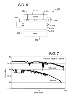
High temperature performance capable gallium nitride transistor
PatentActiveUS20080230786A1
Innovation
- The transistors incorporate a gate electrode made from materials with high Schottky barriers, such as platinum (Pt), tungsten (W), molybdenum (Mo), chromium (Cr), or nickel-chromium alloys (NiCr), and polycrystalline indium nitride, along with spacer layers and field plates to reduce peak electric fields and enhance durability at high temperatures.
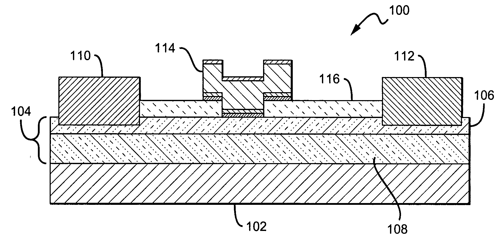
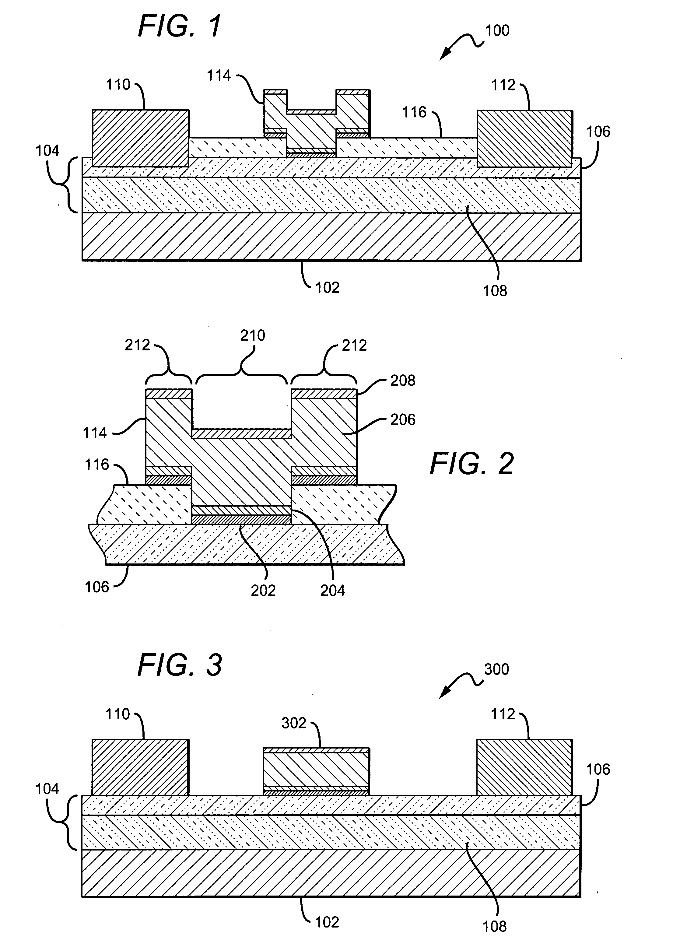
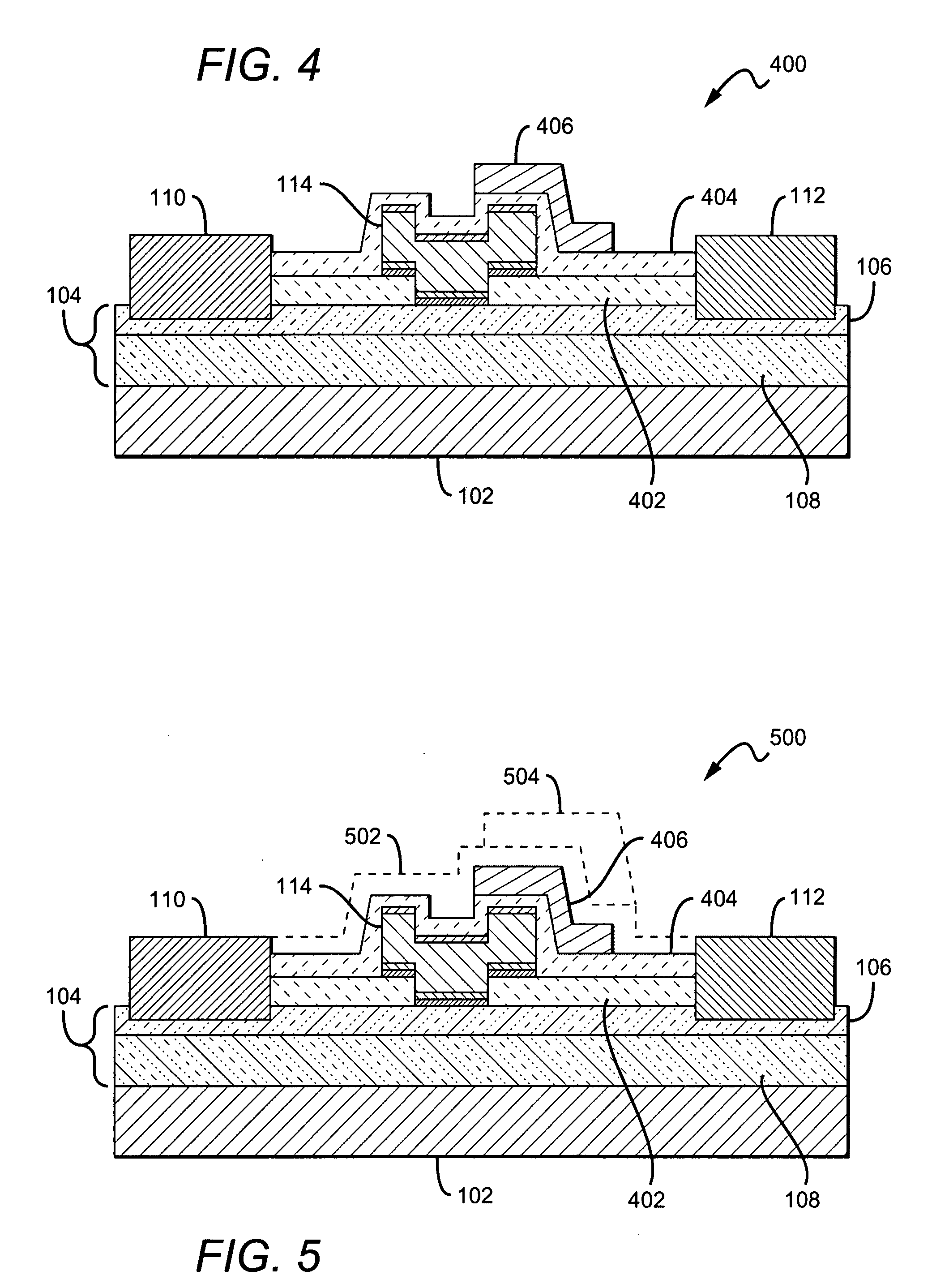
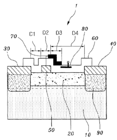
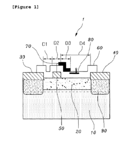
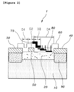
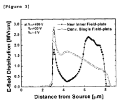
Gallium nitride high electron mobility transistor having inner field-plate for high power applications
PatentInactiveUS7696535B2
Innovation
- Incorporating an inner field-plate between the gate and drain electrodes to distribute the electric field, reduce peak values, and apply varying voltages to the inner field-plate, thereby reducing gate leakage current and capacitance while maintaining high frequency performance.
Reliability Testing Standards for GaN Power Devices
Reliability testing standards for GaN power devices have evolved significantly in response to the unique characteristics and failure mechanisms of these advanced semiconductor components. The Joint Electron Device Engineering Council (JEDEC) has established several standards specifically addressing wide bandgap semiconductors, including JEP180 and JC-70 committees focused on GaN reliability qualification. These standards define rigorous testing protocols that account for the distinctive thermal behavior of GaN HEMTs.
Temperature-dependent testing forms a critical component of these standards, with High Temperature Operating Life (HTOL) tests typically conducted at elevated temperatures (150°C to 175°C) for 1000+ hours to accelerate potential failure mechanisms. This approach is particularly relevant given the significant impact of temperature on GaN HEMT switching performance, where increased temperatures can lead to threshold voltage shifts and reduced carrier mobility.
Dynamic characterization standards have also emerged, requiring devices to undergo switching tests at various temperature conditions to evaluate performance degradation. These tests typically measure switching losses, on-resistance changes, and gate charge variations across temperature ranges from -40°C to 175°C, providing comprehensive data on how temperature affects switching metrics.
Short-circuit robustness testing represents another critical standard area, with protocols defining specific temperature conditions under which devices must withstand short-circuit events. The standards recognize that GaN HEMTs exhibit different temperature-dependent short-circuit withstand capabilities compared to silicon devices, necessitating specialized test methodologies.
Automotive qualification standards (AEC-Q101) have been adapted for GaN power devices, incorporating more stringent temperature cycling requirements (-55°C to 175°C) and humidity-temperature bias testing to account for GaN's unique degradation mechanisms. These modifications acknowledge the critical role temperature plays in GaN HEMT reliability, particularly in demanding automotive applications.
Industry consortia like PowerAmerica and the European ECPE have contributed to standardization efforts by developing application-specific testing guidelines that address temperature-dependent phenomena in GaN switching applications. These guidelines often exceed basic qualification requirements, focusing on mission-profile testing that simulates actual operating conditions including temperature fluctuations encountered in real-world applications.
Thermal Simulation and Modeling Methodologies
Thermal simulation and modeling methodologies have become essential tools for understanding and predicting the thermal behavior of GaN HEMT devices under various operating conditions. These methodologies employ sophisticated computational techniques to analyze heat generation, dissipation, and the resulting temperature distribution within semiconductor devices and their packaging structures.
The most widely adopted approach is Finite Element Analysis (FEA), which discretizes the device structure into small elements and solves heat transfer equations across these elements. Commercial software packages such as ANSYS, COMSOL Multiphysics, and Siemens Simcenter provide robust platforms for implementing FEA-based thermal simulations specifically tailored for power electronics applications. These tools can accurately model complex geometries and material interfaces present in modern GaN HEMT packages.
Compact thermal modeling represents another significant methodology, offering reduced computational complexity while maintaining acceptable accuracy for system-level thermal analysis. These models use thermal resistance networks to approximate the thermal behavior of complex structures, enabling rapid evaluation of different cooling strategies and package designs. The JEDEC standards for compact thermal modeling provide a framework for creating consistent and comparable thermal models across the industry.
Multi-physics simulation approaches have gained prominence as they can simultaneously account for electrical, thermal, and mechanical phenomena. This is particularly valuable for GaN HEMTs where strong coupling exists between electrical performance and temperature. These simulations can predict how switching losses generate heat and how the resulting temperature rise affects subsequent switching events, creating a feedback loop that must be properly characterized.
Recent advances in thermal modeling include the incorporation of machine learning techniques to accelerate simulation processes. Neural networks trained on extensive simulation datasets can predict temperature distributions with remarkable speed, enabling real-time thermal management strategies. Additionally, molecular dynamics simulations are being employed to understand thermal transport at interfaces and in novel materials used in advanced GaN HEMT structures.
Validation methodologies for thermal models typically involve infrared thermal imaging, embedded temperature sensors, and transient thermal testing. These experimental techniques provide crucial reference data for refining simulation parameters and ensuring model accuracy. The development of standardized validation protocols has improved the reliability of thermal simulations across different research groups and commercial entities.
The accuracy of thermal simulations heavily depends on material property data, particularly thermal conductivity values which can vary significantly with temperature. Comprehensive material characterization across the operating temperature range of GaN HEMTs is therefore essential for developing reliable thermal models that can accurately predict device performance under dynamic switching conditions.
Unlock deeper insights with Patsnap Eureka Quick Research — get a full tech report to explore trends and direct your research. Try now!
Generate Your Research Report Instantly with AI Agent
Supercharge your innovation with Patsnap Eureka AI Agent Platform!