Conduction Losses Versus Switching Losses In GaN HEMTs
SEP 5, 20259 MIN READ
Generate Your Research Report Instantly with AI Agent
Patsnap Eureka helps you evaluate technical feasibility & market potential.
GaN HEMT Power Loss Fundamentals and Objectives
Gallium Nitride High Electron Mobility Transistors (GaN HEMTs) have emerged as revolutionary power semiconductor devices, offering significant advantages over traditional silicon-based technologies. The evolution of power electronics has consistently pursued higher efficiency, greater power density, and improved thermal performance, with GaN HEMTs representing a major advancement in this trajectory. These wide-bandgap semiconductor devices have demonstrated exceptional capabilities in high-frequency, high-power applications due to their superior material properties.
Power loss in GaN HEMTs can be categorized into two primary components: conduction losses and switching losses. Conduction losses occur during the on-state of the device and are proportional to the square of the current multiplied by the on-resistance (RDS(on)). GaN's ability to achieve significantly lower on-resistance compared to silicon devices of similar voltage ratings has been a key driver for its adoption in power conversion systems.
Switching losses, on the other hand, occur during the transition between on and off states. These losses are proportional to the switching frequency and are influenced by factors including gate charge, output capacitance, and reverse recovery characteristics. GaN HEMTs exhibit remarkably low gate charge and output capacitance, enabling them to switch at much higher frequencies with reduced losses compared to silicon MOSFETs or IGBTs.
The technical evolution of GaN power devices has been marked by continuous improvements in epitaxial growth techniques, device architecture, and packaging technologies. Early GaN HEMTs suffered from reliability issues and relatively high costs, limiting their commercial viability. However, advancements in manufacturing processes have steadily addressed these challenges, leading to more robust and cost-effective devices.
The primary technical objective in GaN HEMT development has been to optimize the balance between conduction and switching losses across various operating conditions. This optimization is crucial for maximizing overall system efficiency in applications ranging from power supplies and motor drives to renewable energy systems and electric vehicle chargers.
Recent research has focused on novel gate drive techniques, improved thermal management solutions, and advanced packaging methods to further enhance GaN HEMT performance. The development of enhancement-mode (normally-off) GaN HEMTs has been particularly significant, as it simplifies gate drive requirements and improves system safety compared to depletion-mode (normally-on) devices.
Understanding the fundamental trade-offs between conduction and switching losses is essential for designing optimal GaN-based power conversion systems. As operating frequencies increase, switching losses typically become more dominant, necessitating careful consideration of circuit topologies and control strategies to fully leverage GaN's capabilities while maintaining thermal stability and reliability.
Market Demand Analysis for High-Efficiency Power Electronics
The power electronics market is experiencing unprecedented growth driven by the increasing demand for energy-efficient solutions across multiple sectors. This growth trajectory is particularly evident in applications requiring high-frequency switching capabilities where GaN HEMTs (Gallium Nitride High Electron Mobility Transistors) offer significant advantages over traditional silicon-based technologies. The global power electronics market, currently valued at over 40 billion USD, is projected to grow at a compound annual growth rate of 5.7% through 2028, with wide bandgap semiconductors like GaN representing the fastest-growing segment.
The automotive sector represents one of the most promising markets for GaN technology, particularly in electric vehicle (EV) applications. The EV market is expanding rapidly, with global sales increasing by 40% in 2022 alone. Power converters utilizing GaN HEMTs can significantly improve the efficiency of onboard chargers and DC-DC converters, directly addressing range anxiety concerns by extending battery life through reduced power losses.
Consumer electronics manufacturers are increasingly adopting GaN-based power supplies due to their smaller form factor and higher efficiency. The market for fast chargers has grown substantially, with over 1 billion smartphones shipped annually requiring increasingly powerful yet compact charging solutions. GaN technology, with its superior balance between conduction and switching losses, enables chargers that are 40% smaller while delivering higher power density.
Renewable energy systems represent another critical market for high-efficiency power electronics. The solar inverter market alone is expected to reach 27 billion USD by 2026. The ability of GaN HEMTs to operate efficiently at higher frequencies allows for smaller passive components, reducing overall system size and cost while improving energy harvest rates by 2-3% compared to silicon-based solutions.
Data centers, which currently consume approximately 1-2% of global electricity, are under immense pressure to improve energy efficiency. The server power supply market exceeds 3 billion USD annually, with efficiency improvements directly impacting operating costs. GaN-based power supplies can reduce energy losses by up to 40% compared to silicon alternatives, representing significant operational savings at scale.
Industrial motor drives, which account for nearly 45% of global electricity consumption, present another substantial market opportunity. The precise control of conduction and switching losses in GaN HEMTs enables more efficient variable frequency drives, potentially reducing energy consumption by 10-15% in industrial applications.
The telecommunications infrastructure market, particularly with the ongoing 5G rollout, requires increasingly efficient power solutions for base stations. The market for telecom power systems exceeds 4 billion USD annually, with GaN technology enabling up to 30% reduction in energy consumption while supporting higher power densities needed for compact installations.
Current Challenges in GaN HEMT Loss Characterization
Despite significant advancements in GaN HEMT technology, accurate loss characterization remains a persistent challenge for researchers and engineers. Current methodologies for measuring and distinguishing between conduction and switching losses in GaN HEMTs suffer from several limitations that impede precise performance evaluation and optimization.
The high switching speeds of GaN devices, often exceeding 100 V/ns, create substantial measurement difficulties. Conventional equipment struggles to capture transient events occurring in nanosecond timeframes, leading to incomplete or distorted loss profiles. This challenge is particularly pronounced when attempting to isolate switching losses from overall system losses.
Temperature dependency further complicates loss characterization. GaN HEMTs exhibit dynamic RDS(on) behavior that varies significantly with temperature, creating a moving target for conduction loss assessment. The thermal coupling between conduction and switching phenomena means that each loss mechanism influences the other, making isolated measurements problematic.
Parasitic elements present another major obstacle. The ultrafast switching capabilities of GaN devices make them extremely sensitive to circuit parasitics, including PCB layout, gate driver characteristics, and measurement probe positioning. These parasitics can dramatically alter switching waveforms and associated losses, yet are difficult to account for in standardized testing procedures.
Cross-verification between different measurement techniques reveals concerning inconsistencies. Calorimetric methods, electrical double-pulse testing, and simulation-based approaches often yield divergent results for the same device under identical operating conditions. This lack of measurement consensus undermines confidence in performance comparisons between different GaN technologies.
The dynamic interplay between conduction and switching losses presents perhaps the most fundamental challenge. As switching frequency increases, the relationship between these loss components becomes increasingly complex and interdependent. Traditional loss models that treat these mechanisms as separate, additive components fail to capture this complexity.
Current industry standards and testing protocols remain inadequately adapted to GaN's unique characteristics. Most were developed for silicon devices with significantly different switching behaviors and loss profiles. This standardization gap creates barriers to meaningful benchmarking across different manufacturers and device generations.
Advanced modeling approaches that accurately predict the balance between conduction and switching losses across diverse operating conditions are still evolving. Existing models often rely on simplifications that become invalid at GaN's operating extremes, particularly at high frequencies and under hard-switching conditions.
Existing Methodologies for GaN HEMT Loss Reduction
01 GaN HEMT device structures for reducing losses
Specific structural designs of GaN HEMTs can significantly reduce both conduction and switching losses. These designs include optimized gate structures, improved channel designs, and novel substrate materials that enhance electron mobility while reducing parasitic capacitances. Such structural optimizations lead to lower on-resistance during conduction and faster switching transitions, resulting in overall improved efficiency for power conversion applications.- GaN HEMT device structures for reducing losses: Gallium Nitride High Electron Mobility Transistors (GaN HEMTs) can be designed with specific structural features to minimize both conduction and switching losses. These designs include optimized gate structures, improved channel materials, and enhanced electron mobility layers. By engineering the device architecture, manufacturers can reduce on-resistance which directly impacts conduction losses, while also improving charge distribution to minimize switching losses during high-frequency operation.
- Driving and control techniques for GaN HEMTs: Advanced driving and control techniques can significantly reduce switching losses in GaN HEMTs. These include optimized gate driving circuits, precise timing control, and adaptive driving strategies that adjust to operating conditions. Implementing proper dead-time management and gate voltage control helps minimize losses during switching transitions. These techniques leverage the high-speed capabilities of GaN while preventing excessive power dissipation during state changes.
- Thermal management solutions for GaN HEMTs: Effective thermal management is crucial for minimizing conduction losses in GaN HEMTs. Various cooling strategies, including advanced packaging techniques, heat spreading materials, and thermal interface materials, help dissipate heat generated during operation. By maintaining lower junction temperatures, the device's on-resistance remains lower, directly reducing conduction losses. Improved thermal designs also allow GaN HEMTs to operate at higher power densities without performance degradation.
- Power conversion topologies optimized for GaN HEMTs: Specialized power conversion topologies can be designed to leverage GaN HEMTs' unique characteristics while minimizing both conduction and switching losses. These include soft-switching techniques, resonant converters, and multi-level converter designs that reduce voltage stress and switching transitions. By operating GaN devices in their optimal regions and minimizing hard-switching events, these topologies significantly improve efficiency in power conversion applications.
- Measurement and characterization methods for GaN HEMT losses: Accurate measurement and characterization techniques are essential for understanding and optimizing GaN HEMT losses. These methods include specialized test setups for dynamic on-resistance measurement, switching energy evaluation, and temperature-dependent performance analysis. Advanced instrumentation and testing protocols help identify loss mechanisms under various operating conditions, enabling targeted improvements in device design and application. These techniques provide valuable insights for developing more efficient GaN HEMT-based power systems.
02 Driving and control techniques for GaN HEMTs
Advanced gate driving and control techniques can minimize both conduction and switching losses in GaN HEMTs. These techniques include optimized gate voltage control, precise timing of switching transitions, and adaptive driving methods that respond to operating conditions. By implementing sophisticated control algorithms and driver circuits specifically designed for GaN characteristics, the devices can operate closer to their theoretical performance limits with reduced losses.Expand Specific Solutions03 Thermal management solutions for GaN HEMTs
Effective thermal management is crucial for minimizing conduction losses in GaN HEMTs, as device performance degrades at elevated temperatures. Various cooling techniques and packaging solutions have been developed to efficiently dissipate heat from these devices. These include advanced thermal interface materials, optimized heat sink designs, and innovative packaging approaches that reduce thermal resistance. Better thermal management allows GaN HEMTs to maintain lower on-resistance during operation.Expand Specific Solutions04 Circuit topologies optimized for GaN HEMTs
Specialized power converter topologies can leverage the unique characteristics of GaN HEMTs to minimize both conduction and switching losses. These circuit designs often incorporate soft-switching techniques, resonant operation modes, and optimized magnetic components that work synergistically with GaN devices. By operating GaN HEMTs under favorable conditions and utilizing their fast switching capabilities appropriately, these topologies achieve higher efficiency than conventional designs.Expand Specific Solutions05 Measurement and characterization methods for GaN HEMT losses
Accurate measurement and characterization techniques are essential for understanding and optimizing GaN HEMT losses. These methods include specialized test setups for dynamic on-resistance measurement, high-speed switching characterization, and temperature-dependent parameter extraction. Advanced modeling approaches based on these measurements help designers predict device behavior under various operating conditions, enabling them to make informed design decisions that minimize both conduction and switching losses in practical applications.Expand Specific Solutions
Key Industry Players in GaN HEMT Technology
The GaN HEMT market is currently in a growth phase, with increasing adoption driven by the technology's superior performance in balancing conduction and switching losses compared to traditional silicon devices. The global market for GaN power devices is projected to reach $1.5 billion by 2026, with a CAGR of approximately 35%. Leading companies like Wolfspeed, GaN Systems, and Innoscience are advancing GaN HEMT technology through innovations in device structure and packaging to further reduce both conduction and switching losses. Established semiconductor manufacturers including Texas Instruments, Infineon, and STMicroelectronics are also investing heavily in GaN technology, while research institutions such as Nanjing University and HKUST are exploring novel approaches to optimize the conduction-switching loss trade-off, indicating the technology is approaching mainstream commercial maturity.
Wolfspeed, Inc.
Technical Solution: Wolfspeed has developed advanced GaN HEMT designs that specifically address the conduction versus switching losses trade-off. Their technology utilizes a proprietary high-electron mobility transistor structure with optimized gate design and channel engineering to reduce on-resistance (RDS(on)) while maintaining fast switching capabilities. Wolfspeed's approach includes specialized field plate structures that help redistribute the electric field to minimize both dynamic RDS(on) and switching losses. Their latest generation devices incorporate advanced epitaxial layer structures with optimized buffer layers to reduce trapping effects that contribute to dynamic RDS(on) increase. Additionally, Wolfspeed has implemented innovative gate driver solutions that provide precise control of switching transitions, allowing users to balance conduction and switching losses according to specific application requirements.
Strengths: Superior material quality and vertical integration allowing for optimized device structures; excellent high-frequency performance with minimal switching losses; industry-leading power density. Weaknesses: Higher cost compared to silicon alternatives; requires more complex gate drive circuitry to fully optimize the conduction-switching loss trade-off.
Innoscience (Zhuhai) Technology Co., Ltd.
Technical Solution: Innoscience has pioneered an innovative approach to balancing conduction and switching losses in GaN HEMTs through their proprietary "InnoGaN" technology platform. Their solution features an optimized lateral device structure with enhanced channel mobility and reduced parasitic capacitances. Innoscience's technology incorporates a unique buffer layer design that minimizes electron trapping effects, which significantly reduces dynamic RDS(on) - a critical factor affecting conduction losses. Their devices utilize advanced field plate structures that effectively distribute the electric field, allowing for higher breakdown voltage while maintaining low on-resistance. Innoscience has also developed specialized gate designs that enable faster switching transitions with reduced Miller effect, thereby minimizing switching losses. Their manufacturing process employs 8-inch silicon wafers, enabling cost-effective production while maintaining high performance characteristics that address the conduction-switching loss balance.
Strengths: Cost-effective high-volume manufacturing capability on 8-inch silicon wafers; excellent balance of performance and cost; strong integration potential for power system applications. Weaknesses: Relatively newer to the market compared to established competitors; thermal management challenges in high-power density applications.
Critical Technologies for Balancing Conduction and Switching Losses
IRRADIATION-RESISTANT GaN HEMT WITH DECOUPLING REVERSE CONDUCTION CAPABILITY AND FABRICATING METHOD THEREOF
PatentPendingUS20250169162A1
Innovation
- An irradiation-resistant GaN HEMT with decoupling reverse conduction capability is developed, featuring a built-in reverse freewheeling diode formed by connecting a portion of the gate to the source, and utilizing Schottky metal at both ends to prevent gate leakage, thereby decoupling reverse turn-on voltage from forward threshold voltage.
Gallium nitride high electron mobility transistor with ledges and field plates
PatentWO2020033038A1
Innovation
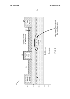
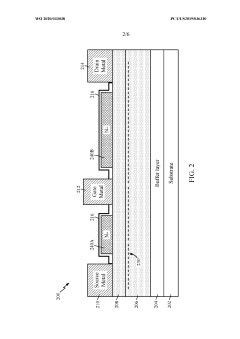
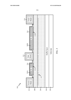
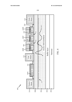
- Incorporating n-doped protuberances, or ledges, between the gate and source/drain electrodes, and optionally using field plates, to reduce surface states and increase channel electron density, thereby enhancing breakdown voltage and switching efficiency.
Thermal Management Strategies for GaN HEMT Applications
Effective thermal management is critical for GaN HEMT applications due to the significant heat generation during device operation. The thermal challenges arise primarily from two main loss mechanisms: conduction losses and switching losses, which contribute differently to the overall thermal profile of GaN devices.
Conduction losses in GaN HEMTs occur during the ON-state when current flows through the device, generating heat proportional to the square of the current multiplied by the on-resistance (RDS(on)). While GaN inherently offers lower RDS(on) compared to silicon counterparts, these losses still constitute a substantial portion of the total thermal budget, especially in high-current applications.
Switching losses, conversely, manifest during state transitions and scale with switching frequency. These losses result from charging and discharging of parasitic capacitances and are particularly significant in high-frequency applications where GaN devices excel. The extremely fast switching capability of GaN HEMTs (sub-nanosecond range) creates concentrated thermal spikes that require specialized management strategies.
The balance between conduction and switching losses dictates optimal thermal management approaches. For high-current, lower-frequency applications where conduction losses dominate, strategies focus on reducing thermal resistance from junction to case through advanced packaging techniques like direct bonded copper (DBC) substrates or embedded die technology. These approaches maximize heat spreading from the active device region.
For high-frequency applications where switching losses predominate, thermal management strategies emphasize transient thermal response. Techniques include integrating phase-change materials that absorb thermal spikes, implementing pulsed operation protocols, and utilizing advanced gate driving schemes that optimize switching trajectories to minimize losses during transitions.
Novel composite thermal interface materials (TIMs) with directionally-enhanced thermal conductivity are emerging as effective solutions that address both loss mechanisms. These materials feature tailored thermal pathways that efficiently extract heat from specific device regions where either conduction or switching losses concentrate.
Active cooling solutions, including microfluidic channels integrated directly into GaN HEMT packages, represent the cutting edge of thermal management. These systems can dynamically adjust cooling capacity based on real-time monitoring of device temperature profiles, effectively addressing the distinct thermal signatures of both conduction and switching losses.
The industry trend is moving toward holistic thermal design approaches that consider the entire power conversion system rather than focusing solely on device-level thermal management. This system-level perspective enables optimized trade-offs between conduction and switching losses through coordinated thermal strategies across components.
Reliability and Lifetime Considerations in GaN HEMT Design
Reliability and lifetime considerations represent critical factors in the design and application of GaN HEMTs, particularly when balancing conduction and switching losses. The inherent material properties of GaN that enable high-frequency operation and lower losses also introduce unique reliability challenges that must be addressed through careful design considerations.
The reliability of GaN HEMTs is significantly influenced by the balance between conduction and switching losses. Devices optimized primarily for low conduction losses may experience increased thermal stress during switching events, while those designed to minimize switching losses might suffer from higher steady-state thermal loads. This trade-off directly impacts the mean time to failure (MTTF) and overall lifetime of the device.
Temperature-dependent degradation mechanisms present a particular concern in GaN HEMT reliability. The relationship between junction temperature and device lifetime typically follows an Arrhenius relationship, with lifetime decreasing exponentially as temperature increases. Conduction losses contribute to steady-state heating, while switching losses generate transient temperature spikes that can accelerate degradation mechanisms such as electron trapping, gate sinking, and metal migration.
Dynamic Ron effects—where the on-resistance temporarily increases after high-voltage stress—represent another reliability challenge directly related to the conduction-switching loss balance. This phenomenon can lead to unexpected increases in conduction losses during operation, potentially creating a destructive feedback loop where increased losses lead to higher temperatures and further degradation.
Field reliability data indicates that GaN HEMTs designed with balanced loss profiles demonstrate superior lifetime characteristics compared to those optimized exclusively for either conduction or switching performance. Industry standards such as JEDEC JEP180 provide testing methodologies specifically for GaN power devices, addressing both static and dynamic reliability concerns.
Advanced packaging solutions have emerged as critical enablers for GaN HEMT reliability. Innovative thermal management approaches, including double-sided cooling and embedded heat spreading layers, help mitigate the temperature-related reliability issues stemming from both conduction and switching losses. These packaging innovations have extended projected device lifetimes from the 10,000-hour range to beyond 100,000 hours in many applications.
Future reliability improvements will likely focus on novel passivation techniques and buffer layer designs that minimize charge trapping effects while maintaining the favorable loss characteristics of GaN technology. Additionally, the development of more sophisticated condition monitoring systems will enable predictive maintenance strategies based on real-time assessment of device degradation.
Unlock deeper insights with Patsnap Eureka Quick Research — get a full tech report to explore trends and direct your research. Try now!
Generate Your Research Report Instantly with AI Agent
Supercharge your innovation with Patsnap Eureka AI Agent Platform!