Switching Characteristics Of GaN HEMTs Explained
SEP 5, 20259 MIN READ
Generate Your Research Report Instantly with AI Agent
Patsnap Eureka helps you evaluate technical feasibility & market potential.
GaN HEMT Technology Evolution and Objectives
Gallium Nitride (GaN) High Electron Mobility Transistors (HEMTs) have emerged as revolutionary power semiconductor devices, transforming the landscape of power electronics since their initial development in the early 1990s. The evolution of GaN HEMT technology has been characterized by continuous improvements in material quality, device architecture, and manufacturing processes, leading to enhanced performance metrics such as higher breakdown voltage, lower on-resistance, and faster switching speeds.
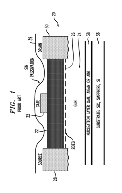
The technological trajectory of GaN HEMTs began with fundamental research into wide bandgap semiconductors, driven by the limitations of silicon-based devices in high-power and high-frequency applications. Early GaN HEMTs faced significant challenges related to substrate quality, epitaxial growth techniques, and reliability issues, particularly dynamic Ron degradation and current collapse phenomena that impacted switching performance.
By the mid-2000s, substantial progress in epitaxial growth techniques, particularly metal-organic chemical vapor deposition (MOCVD), enabled the production of high-quality GaN-on-Si wafers, marking a critical milestone in commercialization efforts. This period also saw the development of various field plate structures and buffer layer designs to mitigate surface-related current collapse and improve breakdown characteristics.
The 2010s witnessed the emergence of enhancement-mode (normally-off) GaN HEMTs through innovations such as p-GaN gates, recessed gate structures, and hybrid cascode configurations. These developments addressed the inherent normally-on characteristic of conventional GaN HEMTs, making them more compatible with existing power electronics systems and safety requirements.
Recent technological advancements have focused on optimizing switching behavior through improved gate drive techniques, package parasitic reduction, and novel device architectures that minimize switching losses. Understanding and controlling the unique switching characteristics of GaN HEMTs has become paramount as operating frequencies continue to increase, pushing the boundaries of power density and efficiency.
The primary objectives of current GaN HEMT research and development include: achieving higher breakdown voltages exceeding 1200V for medium-voltage applications; reducing dynamic Ron effects for improved reliability; minimizing parasitic inductances and capacitances to fully leverage GaN's intrinsic switching speed; developing cost-effective vertical GaN structures; and establishing comprehensive reliability standards specific to GaN technology.
Future evolution paths point toward monolithic integration of GaN power devices with control and protection circuitry, three-dimensional packaging solutions to optimize thermal management, and the development of GaN-specific power electronic topologies that fully exploit the unique switching characteristics of these devices.
Market Demand Analysis for GaN Power Electronics
The global market for Gallium Nitride (GaN) power electronics has experienced remarkable growth in recent years, driven primarily by the increasing demand for high-efficiency power conversion systems. Current market valuations place the GaN power device sector at approximately $1.4 billion in 2023, with projections indicating a compound annual growth rate (CAGR) of 25-30% through 2028. This accelerated growth trajectory significantly outpaces traditional silicon-based power electronics, which typically see single-digit growth rates.
The demand for GaN HEMTs (High Electron Mobility Transistors) is particularly strong in several key application sectors. Consumer electronics represents the largest current market segment, with manufacturers increasingly adopting GaN technology for fast chargers and power adapters. The superior switching characteristics of GaN HEMTs enable smaller form factors and higher power densities, addressing consumer preferences for more compact and efficient charging solutions.
Automotive applications constitute the fastest-growing segment for GaN power electronics. The electric vehicle (EV) market's expansion has created substantial demand for high-efficiency power conversion systems, where GaN HEMTs' switching performance offers significant advantages in onboard chargers, DC-DC converters, and traction inverters. Industry analysts predict that by 2026, approximately 15% of new EVs will incorporate GaN power devices in at least one power system component.
Industrial power systems represent another substantial market opportunity. The industrial sector's focus on energy efficiency and power density has created growing demand for GaN-based motor drives, uninterruptible power supplies, and industrial power supplies. The enhanced switching characteristics of GaN HEMTs directly translate to energy savings and reduced operational costs in these applications.
Renewable energy systems, particularly solar inverters and energy storage systems, have emerged as a promising growth area for GaN power electronics. The higher switching frequencies possible with GaN HEMTs allow for smaller passive components and higher conversion efficiencies, addressing key requirements in distributed energy generation and storage applications.
Market research indicates that regional adoption patterns vary significantly. Asia-Pacific currently leads GaN power electronics consumption, accounting for approximately 45% of the global market, followed by North America at 30% and Europe at 20%. China, Japan, and South Korea have established themselves as both major production centers and consumption markets for GaN power devices.
The market demand is further bolstered by increasingly stringent energy efficiency regulations worldwide. Government initiatives promoting energy conservation and carbon emission reduction have created favorable conditions for GaN adoption across multiple industries, as system designers seek technologies that can meet these regulatory requirements while delivering competitive performance advantages.
Current Switching Performance Challenges in GaN HEMTs
Despite the significant advancements in GaN HEMT technology, several critical challenges persist in their switching performance that limit their full potential in power electronics applications. The primary challenge lies in the dynamic ON-resistance phenomenon, where the device's resistance temporarily increases after switching from a high-voltage OFF-state to an ON-state. This effect, often attributed to charge trapping mechanisms, can significantly degrade efficiency and thermal performance in high-frequency applications.
Another substantial challenge is the presence of parasitic inductances in GaN HEMT packages and circuit layouts. These inductances interact with the extremely fast switching speeds of GaN devices (often exceeding 100 V/ns), resulting in voltage overshoots and ringing that can compromise reliability and increase electromagnetic interference (EMI). The mitigation of these parasitic effects requires specialized packaging technologies and careful circuit design considerations.
Gate driving presents unique challenges for GaN HEMTs compared to traditional silicon devices. The narrower gate voltage margin between enhancement and destruction necessitates precise gate drive circuits with tight voltage control. Additionally, the lower gate charge of GaN HEMTs requires drivers capable of delivering clean, fast transients without oscillations that could trigger false turn-on events or damage the gate structure.
Thermal management remains a significant obstacle, particularly as GaN devices are pushed to higher power densities. The concentrated heat generation in the active region, combined with the thermal boundary resistance between GaN and substrate materials, creates hotspots that can accelerate device degradation. This challenge is exacerbated in high-frequency applications where switching losses contribute significantly to overall heating.
Current collapse effects, resulting from electron trapping in the buffer and surface regions, continue to impact the reliability and performance consistency of GaN HEMTs. These effects manifest as a temporary reduction in drain current capability after high-voltage operation, limiting the device's ability to handle subsequent switching events efficiently.
The lack of standardized reliability testing protocols specifically designed for GaN HEMTs presents an industry-wide challenge. The unique failure mechanisms and operational stresses of these devices differ significantly from silicon technologies, requiring new approaches to qualification and lifetime prediction that account for the specific degradation modes observed in GaN technology.
Finally, cost remains a barrier to widespread adoption, with current GaN HEMT manufacturing processes still more expensive than mature silicon technologies. The challenge lies in developing more cost-effective fabrication techniques while maintaining the performance advantages that make GaN attractive for next-generation power applications.
State-of-the-Art Switching Solutions for GaN HEMTs
01 High-speed switching characteristics of GaN HEMTs
GaN HEMTs exhibit superior high-speed switching characteristics compared to traditional silicon-based transistors. These devices demonstrate faster switching speeds, lower switching losses, and higher efficiency during high-frequency operation. The wide bandgap properties of gallium nitride enable rapid electron mobility in the two-dimensional electron gas (2DEG) channel, resulting in reduced switching times and improved performance in power conversion applications.- Switching speed and efficiency characteristics of GaN HEMTs: GaN HEMTs demonstrate superior switching characteristics compared to traditional silicon-based transistors, including faster switching speeds and reduced switching losses. These devices exhibit high electron mobility in the two-dimensional electron gas (2DEG) channel, allowing for rapid transitions between on and off states. The enhanced switching efficiency is attributed to lower gate capacitance and reduced on-resistance, making GaN HEMTs particularly suitable for high-frequency power conversion applications.
- Gate structure design for improved switching performance: The gate structure design significantly impacts the switching characteristics of GaN HEMTs. Various gate configurations, including recessed gates, field plates, and novel gate dielectric materials, are employed to optimize switching behavior. These design enhancements help control threshold voltage, reduce gate leakage current, and mitigate dynamic on-resistance effects. Advanced gate structures also contribute to better thermal management during high-frequency switching operations, ultimately improving the overall reliability and performance of GaN HEMT devices.
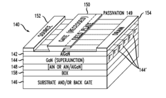
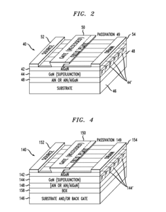
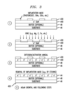
- Buffer layer engineering for enhanced switching characteristics: Buffer layer engineering plays a crucial role in optimizing the switching characteristics of GaN HEMTs. Carefully designed buffer layers help manage current collapse phenomena, reduce trapping effects, and improve breakdown voltage. Multi-layer buffer structures with varying doping profiles and material compositions can effectively control the electric field distribution and charge trapping, resulting in more stable and reliable switching performance. These engineered buffer layers are essential for high-voltage applications where consistent switching behavior is critical.
- Thermal management solutions for high-frequency switching: Thermal management is critical for maintaining optimal switching characteristics in GaN HEMTs, especially during high-frequency operation. Various cooling strategies and package designs are implemented to dissipate heat effectively, preventing performance degradation and ensuring device reliability. Advanced substrate materials with superior thermal conductivity, such as silicon carbide, help improve heat dissipation. Additionally, innovative packaging techniques and integration of heat spreaders contribute to maintaining consistent switching performance under demanding operating conditions.
- Circuit integration and driver design for GaN HEMT switching: Optimizing GaN HEMT switching characteristics requires specialized circuit integration and driver designs. Gate drivers with precise timing control, appropriate voltage levels, and fast transient response are essential for fully leveraging the high-speed switching capabilities of GaN HEMTs. Circuit topologies that minimize parasitic inductances and capacitances help reduce switching losses and ringing effects. Additionally, protection circuits that address the unique characteristics of GaN devices ensure safe operation during various switching conditions, including short circuits and voltage spikes.
02 Gate structure optimization for improved switching
Various gate structure designs have been developed to enhance the switching characteristics of GaN HEMTs. These include recessed gate structures, field plates, and specialized gate dielectrics that help control threshold voltage and reduce gate leakage current. Optimized gate geometries contribute to faster switching speeds by reducing parasitic capacitances and improving gate control over the channel, which leads to sharper transitions between on and off states.Expand Specific Solutions03 Thermal management for reliable switching operation
Effective thermal management is crucial for maintaining reliable switching characteristics in GaN HEMTs. Various approaches include substrate material selection, heat spreading techniques, and package design optimizations that enhance heat dissipation during high-frequency switching operations. Improved thermal performance prevents degradation of switching characteristics under high-power conditions and extends device lifetime by reducing thermal stress during rapid switching cycles.Expand Specific Solutions04 Buffer layer design for reduced switching losses
The buffer layer design significantly impacts the switching performance of GaN HEMTs. Advanced buffer architectures with optimized thickness, doping profiles, and material compositions help minimize current collapse, dynamic on-resistance, and switching losses. These buffer layer innovations improve charge distribution during switching transitions, resulting in more efficient power conversion and reduced switching energy losses in high-frequency applications.Expand Specific Solutions05 Novel device structures for enhanced switching performance
Innovative GaN HEMT device structures have been developed to enhance switching characteristics. These include cascode configurations, hybrid structures, and vertical device architectures that address limitations of conventional lateral HEMTs. Such novel designs optimize the trade-off between on-resistance and breakdown voltage while improving switching speed and reducing parasitic effects, making them suitable for high-frequency power switching applications.Expand Specific Solutions
Leading Manufacturers and Research Institutions in GaN HEMT Industry
The GaN HEMT switching technology market is currently in a growth phase, with increasing adoption across power electronics applications due to superior performance over silicon-based devices. The global market is expanding rapidly, projected to reach significant scale as electric vehicles, renewable energy systems, and 5G infrastructure drive demand. Technologically, companies like Wolfspeed, Texas Instruments, and Infineon lead with mature commercial offerings, while MACOM, QUALCOMM, and ROHM demonstrate strong innovation in high-frequency applications. Research institutions including Nanjing University and HKUST collaborate with industry players like Fujitsu and UMC to address remaining challenges in reliability and cost reduction. The competitive landscape shows established semiconductor giants competing with specialized GaN-focused companies, creating a dynamic ecosystem driving continuous performance improvements.
Wolfspeed, Inc.
Technical Solution: Wolfspeed's GaN HEMT technology focuses on optimizing switching characteristics through advanced gate driver designs and innovative packaging solutions. Their approach addresses critical switching parameters including turn-on/turn-off delays, rise/fall times, and ringing phenomena. Wolfspeed has developed proprietary gate driver ICs specifically designed to control the fast switching speeds of GaN HEMTs, incorporating features like adjustable slew rate control and advanced protection mechanisms. Their latest generation devices achieve switching frequencies exceeding 10MHz with dv/dt rates above 100V/ns while maintaining controlled switching behavior[1]. The company's vertical GaN-on-SiC structure enables higher breakdown voltages (>1200V) compared to lateral GaN-on-Si approaches, with significantly reduced dynamic RDS(on) effects that typically plague GaN switching performance[3]. Wolfspeed's packaging innovations minimize parasitic inductances to below 0.2nH, addressing one of the key challenges in high-frequency GaN switching applications.
Strengths: Superior thermal performance due to SiC substrate; higher breakdown voltage capability; reduced dynamic RDS(on) effects; excellent high-frequency performance. Weaknesses: Higher manufacturing costs compared to Si-based solutions; requires more complex gate drive circuitry; SiC substrate availability constraints can impact production scaling.
Fujitsu Ltd.
Technical Solution: Fujitsu has developed advanced GaN HEMT technology focusing on the fundamental physics of switching behavior and parasitic effects. Their approach implements a proprietary "normally-off" gate structure with optimized field plate designs to control electric field distribution during switching transitions. Fujitsu's technology addresses critical switching parameters through their unique epitaxial layer structure that reduces channel resistance while maintaining high breakdown voltage capability. Their devices achieve switching frequencies exceeding 1MHz with controlled dv/dt rates and minimal ringing[9]. Fujitsu has developed specialized gate driver solutions that incorporate adaptive control algorithms to optimize switching behavior across varying operating conditions. Their packaging technology implements advanced thermal management techniques that enable reliable operation at junction temperatures up to 175°C while maintaining switching performance characteristics[10]. Fujitsu's latest generation devices demonstrate switching energy reductions of approximately 40% compared to silicon alternatives, with particular emphasis on minimizing turn-off losses which typically dominate in GaN HEMT applications.
Strengths: Advanced epitaxial layer technology; excellent high-temperature performance; sophisticated field plate design for electric field management; strong reliability track record. Weaknesses: Less commercial market penetration in power electronics compared to competitors; more limited product portfolio; requires specialized gate drive solutions; higher cost structure than silicon alternatives.
Critical Patents and Research on GaN Switching Mechanisms
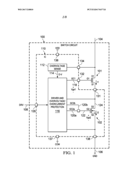
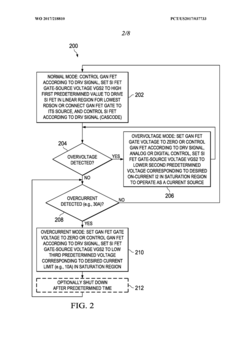
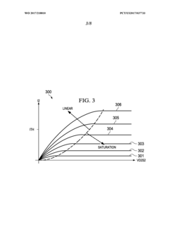
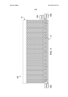
Overvoltage protection and short-circuit withstanding for gallium nitride devices
PatentWO2017218810A1
Innovation
- A driver and current source circuit are integrated with GaN transistors to detect overvoltage and overcurrent conditions, allowing controlled current sinking and cascode configuration to prevent damage, using a low voltage silicon transistor as a current source, either monolithically or in a dual-die configuration, to provide overvoltage and short-circuit protection.
Gallium nitride superjunction devices
PatentInactiveUS20130240951A1
Innovation
- Incorporating a doped gallium nitride superjunction layer with a plurality of p/n junctions between the substrate and a barrier layer, which suppresses breakdown by modifying the electric field distribution, allowing for higher breakdown voltages and enabling the use of low-cost Si substrates.
Thermal Management Strategies for High-Frequency GaN Operation
Thermal management is a critical factor in the operation of GaN HEMTs, particularly when these devices are operated at high frequencies. The superior material properties of GaN, including high thermal conductivity and high breakdown field, make it an excellent candidate for high-power and high-frequency applications. However, these advantages come with significant thermal challenges that must be addressed to ensure optimal device performance and reliability.
The switching characteristics of GaN HEMTs are directly influenced by temperature variations within the device. As operating frequencies increase, the power density and consequent heat generation intensify, potentially leading to thermal runaway conditions if not properly managed. Research indicates that junction temperatures exceeding 150°C can significantly degrade device performance, increasing on-resistance and reducing carrier mobility.
Several thermal management strategies have emerged to address these challenges. Advanced substrate materials such as silicon carbide (SiC) offer superior thermal conductivity compared to traditional silicon substrates, enabling more efficient heat dissipation from the active device region. The thermal conductivity of SiC (approximately 3.7 W/cm·K) significantly outperforms silicon (1.5 W/cm·K), making it particularly valuable for high-frequency GaN HEMT applications.
Innovative packaging solutions also play a crucial role in thermal management. Flip-chip configurations, where the active device layer is mounted face-down on the heat sink, minimize thermal resistance paths and improve heat extraction efficiency. Additionally, advanced thermal interface materials (TIMs) with enhanced thermal conductivity help reduce the thermal boundary resistance between the device and cooling system.
Active cooling techniques represent another important strategy for high-frequency GaN operation. Microfluidic cooling channels integrated directly into device packages can provide localized cooling to hotspots, maintaining more uniform temperature distributions across the device. Some cutting-edge approaches incorporate phase-change materials or two-phase cooling systems that leverage the high heat absorption capacity during phase transitions.
Thermal simulation and modeling have become essential tools in developing effective thermal management strategies. Finite element analysis enables designers to identify potential hotspots and optimize heat flow paths before physical prototyping. These computational approaches help in understanding the complex thermal dynamics during high-frequency switching operations, where transient thermal effects become increasingly significant.
Recent advancements in wide-bandgap semiconductor technology have also focused on device-level thermal optimization. Novel epitaxial layer structures and buffer layer designs help to confine heat generation and facilitate more efficient thermal pathways. Gate field plate structures, while primarily implemented for electric field management, also contribute to more distributed heat generation patterns that prevent localized hotspot formation.
Reliability and Lifetime Assessment of GaN HEMTs Under Switching Stress
The reliability and lifetime assessment of GaN HEMTs under switching stress represents a critical area of investigation for power electronics applications. GaN HEMTs experience significant electrical and thermal stresses during high-frequency switching operations, which can accelerate degradation mechanisms and ultimately lead to device failure.
Switching-induced degradation in GaN HEMTs manifests through several key mechanisms. The high electric fields generated during switching events can cause electron trapping at the AlGaN/GaN interface or in the buffer layers, resulting in threshold voltage shifts and on-resistance increases over time. These trapped charges modify the electric field distribution within the device, potentially accelerating other degradation processes.
Thermal cycling during rapid switching also contributes significantly to reliability concerns. The repeated expansion and contraction of different materials with mismatched thermal expansion coefficients creates mechanical stress at interfaces, particularly between the GaN layers and substrates or packaging materials. This stress can lead to delamination, crack formation, or metal migration in gate and ohmic contacts.
Hot electron effects represent another critical degradation mechanism during switching. When GaN HEMTs switch under high voltage conditions, electrons can gain sufficient energy to overcome potential barriers and become injected into the gate insulator or buffer layers. This phenomenon gradually degrades the gate dielectric integrity and alters the device's threshold voltage characteristics.
Time-dependent dielectric breakdown (TDDB) accelerates under switching conditions due to the repeated application of high electric fields across the gate dielectric. The cumulative effect of these stress events reduces the mean time to failure compared to DC stress conditions, necessitating specialized testing methodologies that accurately replicate real-world switching conditions.
Industry-standard reliability assessment for GaN HEMTs under switching stress typically employs accelerated life testing with controlled temperature, voltage, and switching frequency parameters. These tests aim to identify the activation energies associated with different failure mechanisms and establish acceleration factors that enable lifetime prediction under normal operating conditions.
Advanced characterization techniques including transient electrical measurements, electroluminescence microscopy, and charge pumping methods have emerged as valuable tools for monitoring device degradation during switching stress. These techniques provide insights into the spatial and temporal evolution of defects, allowing for more accurate lifetime modeling and reliability prediction.
Unlock deeper insights with Patsnap Eureka Quick Research — get a full tech report to explore trends and direct your research. Try now!
Generate Your Research Report Instantly with AI Agent
Supercharge your innovation with Patsnap Eureka AI Agent Platform!