GaN HEMT Body Diode Characteristics And Applications
SEP 5, 20259 MIN READ
Generate Your Research Report Instantly with AI Agent
Patsnap Eureka helps you evaluate technical feasibility & market potential.
GaN HEMT Evolution and Research Objectives
Gallium Nitride (GaN) High Electron Mobility Transistors (HEMTs) have emerged as revolutionary power semiconductor devices over the past three decades. The evolution of GaN HEMT technology began in the early 1990s with fundamental research on wide bandgap semiconductors, initially focused on military and aerospace applications due to their superior radiation hardness and high-frequency performance.
The technological trajectory of GaN HEMTs has been marked by significant milestones. In the early 2000s, researchers successfully demonstrated the first commercial-grade GaN HEMTs, primarily targeting RF applications. By the mid-2000s, advancements in epitaxial growth techniques and device fabrication processes enabled the development of GaN HEMTs for power electronics applications, offering unprecedented switching speeds and power density.
A pivotal development occurred around 2010 with the introduction of enhancement-mode GaN HEMTs (e-mode), addressing the normally-on limitation of conventional depletion-mode devices. This innovation significantly expanded the application scope of GaN technology in power conversion systems, making it more compatible with existing circuit topologies and safety requirements.
The body diode characteristics of GaN HEMTs represent a unique aspect of their operation that fundamentally differs from traditional silicon MOSFETs. Unlike silicon devices with intrinsic PN junction body diodes, GaN HEMTs exhibit a reverse conduction mechanism based on the bidirectional current flow capability of the two-dimensional electron gas (2DEG) channel. This characteristic has profound implications for circuit design, particularly in applications requiring synchronous rectification.
Current research objectives in GaN HEMT body diode characteristics focus on several critical areas. First, understanding and modeling the dynamic behavior of reverse conduction, including the impact of trapping effects on reverse recovery performance. Second, optimizing the trade-off between forward voltage drop during reverse conduction and overall device efficiency. Third, developing innovative gate driver solutions that can effectively leverage the unique reverse conduction properties of GaN HEMTs.
The technology trend indicates a growing emphasis on monolithic integration of GaN power devices with control and protection functions, potentially revolutionizing power module design. Additionally, there is significant interest in developing novel circuit topologies specifically optimized for GaN HEMT characteristics, moving beyond simple silicon-to-GaN substitution approaches.
Our research aims to comprehensively characterize the body diode behavior of state-of-the-art GaN HEMTs across various operating conditions, develop accurate behavioral models for circuit simulation, and explore innovative application circuits that can maximize the benefits of GaN HEMT's unique reverse conduction properties while mitigating their limitations.
Market Analysis for GaN HEMT Applications
The global market for GaN HEMT (Gallium Nitride High Electron Mobility Transistor) applications has experienced significant growth in recent years, driven by increasing demand for high-power, high-frequency electronic devices across multiple industries. The market value reached approximately $1.4 billion in 2022 and is projected to grow at a compound annual growth rate (CAGR) of 23% through 2028, potentially reaching $5.2 billion by the end of the forecast period.
Power electronics represents the largest application segment, accounting for over 45% of the total GaN HEMT market. This dominance stems from GaN's superior performance characteristics compared to traditional silicon-based solutions, particularly in high-voltage applications. The body diode characteristics of GaN HEMTs, which exhibit lower reverse recovery charge and faster switching capabilities, have become a critical differentiator in this market segment.
The automotive sector has emerged as one of the fastest-growing markets for GaN HEMT technology, with electric vehicle (EV) applications showing particular promise. On-board chargers, DC-DC converters, and traction inverters all benefit from the enhanced efficiency and reduced size that GaN HEMTs provide. Market analysis indicates that automotive applications could grow at a CAGR of 29% through 2028, outpacing the overall market growth rate.
Telecommunications infrastructure, particularly for 5G deployment, represents another significant market opportunity. The RF characteristics of GaN HEMTs make them ideal for high-frequency, high-power applications in base stations. This segment currently accounts for approximately 25% of the total market and is expected to maintain steady growth as global 5G infrastructure continues to expand.
Consumer electronics applications, including fast chargers for mobile devices and laptops, have seen rapid adoption of GaN HEMT technology. This market segment has grown by 35% year-over-year since 2020, driven by consumer demand for smaller, more efficient charging solutions. The body diode characteristics of GaN HEMTs enable the development of chargers that are up to 40% smaller than silicon-based alternatives while delivering equivalent or superior performance.
Regional analysis shows that Asia-Pacific dominates the GaN HEMT market with approximately 45% market share, followed by North America (30%) and Europe (20%). China, Japan, and South Korea are leading the manufacturing capacity expansion for GaN devices, while significant R&D investments continue in the United States and Europe, particularly focused on improving body diode characteristics for specialized applications.
The competitive landscape features both established semiconductor manufacturers and specialized GaN technology companies. Key market challenges include cost reduction requirements, reliability concerns in certain applications, and the need for standardized characterization methods for body diode performance.
Current Body Diode Challenges in GaN HEMTs
Despite the promising advantages of GaN HEMTs in power electronics, their body diode characteristics present significant challenges that impede widespread adoption. Unlike silicon MOSFETs with inherent PN junction body diodes, GaN HEMTs feature a reverse conduction mechanism through the two-dimensional electron gas (2DEG) channel. This fundamental difference creates several critical issues that designers must address.
The most prominent challenge is the high forward voltage drop during reverse conduction. GaN HEMTs typically exhibit a forward voltage of 1.5-3V compared to silicon MOSFETs' 0.7-1V, resulting in substantially higher conduction losses during dead-time periods in switching applications. This efficiency penalty becomes particularly problematic in applications requiring frequent synchronous rectification.
Dynamic characteristics present another significant hurdle. GaN HEMT body diodes suffer from poor reverse recovery behavior, with substantial variations in performance depending on operating conditions. The reverse recovery charge, though generally lower than silicon counterparts, exhibits inconsistent behavior across temperature ranges and switching frequencies, complicating circuit design and reliability predictions.
Thermal management during reverse conduction poses additional challenges. The higher forward voltage drop generates more heat during body diode conduction, creating localized hot spots that can accelerate device degradation. This thermal stress is particularly concerning in high-frequency applications where body diode conduction occurs frequently, even if briefly.
Reliability issues further compound these challenges. GaN HEMTs demonstrate degradation mechanisms specifically related to reverse conduction stress, including threshold voltage shifts and increased dynamic on-resistance. These reliability concerns are exacerbated by the limited industry-wide standardization of reliability testing protocols specifically addressing body diode operation.
Application-specific challenges emerge in various circuit topologies. In half-bridge configurations, the body diode's higher forward voltage necessitates precise dead-time management to minimize losses. For motor drive applications, the inconsistent reverse recovery characteristics complicate control strategies and efficiency optimization.
Manufacturing variability introduces additional complexity, as body diode characteristics can vary significantly between devices from different manufacturers and even between production batches from the same vendor. This variability complicates design margins and may require more conservative approaches to ensure reliable operation across all conditions.
Addressing these challenges requires innovative circuit techniques, improved device structures, and advanced control strategies to fully leverage GaN HEMT capabilities while mitigating the limitations of their body diode characteristics.
Mainstream Body Diode Implementation Approaches
01 Body diode characteristics and reverse recovery behavior in GaN HEMTs
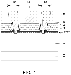
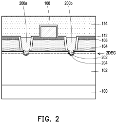
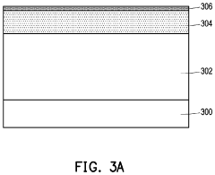
GaN HEMTs exhibit unique body diode characteristics compared to traditional silicon devices. The reverse recovery behavior of these body diodes is characterized by significantly reduced reverse recovery charge and faster recovery times. This results in lower switching losses and improved efficiency in power conversion applications. The inherent properties of the GaN material and device structure contribute to these superior reverse recovery characteristics, making GaN HEMTs particularly suitable for high-frequency switching applications.- Body diode characteristics and reverse conduction mechanisms in GaN HEMTs: GaN HEMTs exhibit unique body diode characteristics due to their lateral device structure. Unlike traditional silicon devices, GaN HEMTs don't have a parasitic body diode but instead feature reverse conduction mechanisms through the two-dimensional electron gas (2DEG) channel. This reverse conduction behavior affects switching performance and reliability, particularly in bridge circuit configurations. Understanding these characteristics is crucial for optimizing device performance in power conversion applications.
- Temperature effects on GaN HEMT body diode behavior: Temperature significantly impacts the reverse conduction characteristics of GaN HEMTs. As temperature increases, the reverse voltage drop typically decreases due to changes in carrier mobility and concentration in the 2DEG channel. This temperature dependence affects the device's switching losses and reliability during reverse conduction events. Thermal management strategies must account for these temperature-dependent characteristics to ensure optimal performance in high-power applications.
- Dynamic characteristics and switching behavior of GaN HEMT body diodes: The dynamic characteristics of GaN HEMT body diodes significantly impact switching performance in power conversion systems. These devices exhibit unique turn-on and turn-off behaviors with minimal reverse recovery charge compared to silicon devices. However, they may display dynamic Ron effects and current collapse phenomena that affect reverse conduction. Advanced gate drive techniques and circuit designs can optimize these dynamic characteristics to reduce switching losses and improve efficiency.
- Enhancement-mode GaN HEMT body diode characteristics: Enhancement-mode (normally-off) GaN HEMTs have distinct body diode characteristics compared to depletion-mode devices. These devices typically employ various gate structures such as p-GaN, recessed gates, or hybrid designs to achieve normally-off operation, which affects their reverse conduction behavior. The threshold voltage and gate design significantly influence the reverse conduction voltage drop and current capability. Understanding these characteristics is essential for designing efficient power conversion circuits using enhancement-mode GaN HEMTs.
- Circuit applications and considerations for GaN HEMT body diode characteristics: The unique body diode characteristics of GaN HEMTs require special consideration in circuit design. In applications like synchronous rectification, half-bridge configurations, and motor drives, the reverse conduction behavior affects dead-time management, efficiency, and reliability. Circuit designers must account for the higher forward voltage drop during reverse conduction compared to silicon MOSFETs. Advanced driving schemes, including third quadrant operation techniques and adaptive dead-time control, can optimize performance by leveraging the unique reverse conduction properties of GaN HEMTs.
02 Temperature dependence of GaN HEMT body diode performance
The body diode characteristics of GaN HEMTs show distinct temperature-dependent behavior. As temperature increases, the forward voltage drop of the body diode typically decreases due to increased carrier concentration, while the reverse leakage current may increase. The temperature coefficient of the body diode voltage is an important parameter for thermal design considerations. Understanding these temperature dependencies is crucial for designing reliable power conversion systems that operate across wide temperature ranges.Expand Specific Solutions03 Structural modifications to enhance body diode performance
Various structural modifications can be implemented in GaN HEMTs to enhance body diode performance. These include optimizing the gate-to-drain spacing, implementing field plates, modifying the buffer layer design, and engineering the channel-barrier interface. Such modifications aim to reduce the forward voltage drop, minimize reverse leakage current, and improve the overall reliability of the body diode. Advanced epitaxial growth techniques and novel device architectures play a significant role in achieving these improvements.Expand Specific Solutions04 Dynamic characteristics and switching behavior of GaN HEMT body diodes
The dynamic characteristics of GaN HEMT body diodes significantly impact their switching behavior. These include turn-on and turn-off transients, voltage overshoot during switching events, and current distribution patterns. The absence of minority carrier storage effects in GaN HEMTs leads to minimal reverse recovery losses compared to silicon devices. Understanding these dynamic characteristics is essential for optimizing gate drive circuits, minimizing switching losses, and preventing device failures in high-frequency power conversion applications.Expand Specific Solutions05 Reliability and degradation mechanisms of GaN HEMT body diodes
The reliability of GaN HEMT body diodes is influenced by various degradation mechanisms. These include hot electron effects, time-dependent dielectric breakdown, and trapping phenomena at the interface and in the buffer layer. Repetitive hard switching events can accelerate degradation, affecting the forward voltage drop and reverse leakage characteristics over time. Comprehensive reliability testing methodologies and lifetime prediction models are essential for ensuring the long-term stability of GaN HEMT body diodes in power electronic applications.Expand Specific Solutions
Leading Manufacturers and Research Institutions
The GaN HEMT body diode characteristics and applications market is currently in a growth phase, with increasing adoption across power electronics sectors. The market is expanding rapidly, projected to reach significant value as GaN technology matures from early adoption to mainstream implementation. Universities (MIT, UESTC, HKUST) are driving fundamental research, while established semiconductor companies (Infineon, Wolfspeed, Texas Instruments) are commercializing products. Emerging specialists like Cambridge GaN Devices and Hunan Sanan are focusing exclusively on GaN innovation. The technology is approaching maturity in power conversion applications, with companies like Huawei Digital Power and DENSO implementing GaN HEMTs in automotive and renewable energy systems, though body diode characteristics optimization remains an active research area.
Infineon Technologies Austria AG
Technical Solution: Infineon has developed CoolGaN™ technology that addresses the unique body diode characteristics of GaN HEMTs through innovative device architecture and manufacturing processes. Their approach focuses on optimizing the reverse conduction behavior of enhancement-mode GaN HEMTs to provide reliable operation in hard-switching applications. Infineon's technology utilizes a p-GaN gate structure that enables normally-off operation while carefully managing the trade-offs between on-resistance, gate reliability, and reverse conduction performance. Their devices feature specialized buffer layer designs that minimize dynamic on-resistance effects while maintaining good body diode characteristics. Infineon has implemented specific edge termination structures that enhance device robustness during reverse conduction events. Their CoolGaN™ devices demonstrate forward voltage drops of approximately 2-3V during reverse conduction, with minimal reverse recovery charge, enabling efficient operation in bridge configurations at switching frequencies exceeding 100kHz. Infineon has also developed comprehensive application guidelines for utilizing GaN HEMT body diode characteristics in various power conversion topologies.
Strengths: Mature manufacturing process with high reliability and robustness during reverse conduction events. Comprehensive design ecosystem and application support for implementing GaN solutions. Weaknesses: Higher forward voltage drop during reverse conduction compared to silicon devices, requiring careful circuit design to optimize efficiency in applications with significant third-quadrant operation.
Cambridge GaN Devices Ltd.
Technical Solution: Cambridge GaN Devices (CGD) has pioneered an innovative approach to GaN HEMT body diode characteristics with their ICeGaN™ technology. Their solution addresses the inherent challenges of GaN HEMTs' intrinsic body diodes by implementing an integrated silicon MOSFET-like driving mechanism that enables safe and reliable operation. CGD's technology features a specialized gate drive architecture that effectively manages the third quadrant operation (reverse conduction mode) of GaN HEMTs, significantly reducing the forward voltage drop during body diode conduction. Their devices incorporate proprietary circuitry that provides built-in protection against voltage spikes and ensures controlled switching behavior. This integrated approach eliminates the need for complex external gate drive circuits while maintaining the performance benefits of GaN technology. CGD has demonstrated devices with body diode forward voltages below 2V and minimal reverse recovery effects, making them particularly suitable for applications requiring bidirectional power flow.
Strengths: Simplified driving requirements similar to silicon MOSFETs, reducing system complexity and enabling drop-in replacement in existing designs. Integrated protection features enhance reliability during body diode conduction. Weaknesses: Slightly higher on-resistance compared to some competing GaN solutions, and limited high-current portfolio compared to more established manufacturers.
Key Patents and Innovations in GaN HEMT Diodes
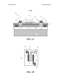
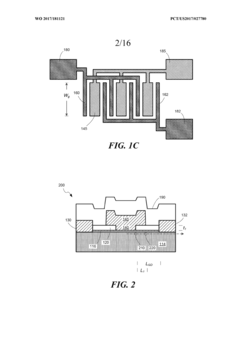
Gallium nitride device and method for manufacturing high electron mobility transistor
PatentPendingUS20240038847A1
Innovation
- The implementation of ohmic sidewall dams and a specific structure for the source and drain, including titanium nitride protrusions and a gold-containing layer, which directly contact the two-dimensional electron gas, reduces contact resistance and blocks leakage paths, thereby improving electrical properties and suppressing the hump phenomenon.
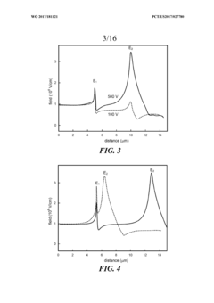
High-voltage GAN high electron mobility transistors
PatentWO2017181121A2
Innovation
- The development of high-voltage HEMTs with a gallium-nitride material structure, including a buffer layer, conduction layer, barrier layer, gate, source, and drain, with a gate-connected field plate extending beyond the gate edges, and a thin gallium-oxide layer formed through oxygen plasma treatment, to enhance reverse-bias voltage withstand and reduce leakage currents.

Thermal Management Considerations for GaN HEMTs
Thermal management is a critical aspect of GaN HEMT design and operation, particularly when considering the body diode characteristics and their applications. GaN HEMTs operate at significantly higher power densities compared to silicon-based devices, which results in concentrated heat generation within a smaller area. This thermal concentration can dramatically affect the body diode performance, reliability, and overall device efficiency.
The thermal conductivity of GaN (approximately 130 W/m·K) is superior to silicon but inferior to silicon carbide, creating unique thermal management challenges. When the body diode is conducting, especially during dead-time periods in switching applications, localized heating occurs at the junction. This heating can alter the forward voltage characteristics of the body diode and potentially accelerate degradation mechanisms if not properly managed.
Temperature rise during body diode conduction affects several key parameters including on-resistance, threshold voltage, and reverse recovery characteristics. Research has shown that the dynamic RDS(on) of GaN HEMTs can increase by 10-20% for every 25°C rise in junction temperature, directly impacting efficiency in applications utilizing the body diode functionality.
Advanced thermal simulation tools have become essential for predicting temperature distributions across GaN HEMT structures during body diode operation. Finite element analysis (FEA) models that incorporate both electrical and thermal physics are particularly valuable for optimizing device designs and packaging solutions to manage heat effectively during body diode conduction events.
Package selection plays a crucial role in thermal management for GaN HEMTs. Traditional packages with wire bonds introduce thermal resistances that can be detrimental to body diode performance. Advanced packaging technologies such as flip-chip assemblies and direct copper bonded (DCB) substrates provide superior thermal pathways, reducing junction temperatures during body diode operation by up to 30% compared to conventional packages.
Active cooling strategies must be tailored specifically for applications heavily utilizing the GaN HEMT body diode. Liquid cooling solutions have demonstrated the ability to maintain junction temperatures below critical thresholds even during high-frequency switching operations where body diode conduction occurs repeatedly. Some cutting-edge designs incorporate microfluidic channels directly into the device substrate, achieving thermal resistances below 0.1°C/W.
The relationship between thermal management and body diode reliability is particularly important for long-term applications. Accelerated life testing has revealed that every 10°C reduction in operating temperature can potentially double the expected lifetime of the body diode functionality, highlighting the critical importance of effective thermal design in GaN HEMT applications.
Reliability and Lifetime Assessment Methods
The reliability assessment of GaN HEMT body diodes requires comprehensive methodologies that differ from traditional silicon devices due to their unique material properties and operational characteristics. Accelerated life testing serves as a cornerstone approach, subjecting devices to elevated temperatures, voltages, and current densities to induce failure mechanisms that might otherwise take years to manifest under normal operating conditions. These tests typically follow industry standards such as JEDEC JESD22 while incorporating GaN-specific modifications.
Time-dependent dielectric breakdown (TDDB) testing has emerged as particularly relevant for GaN HEMTs, as it evaluates the degradation of gate insulation and channel regions under prolonged electrical stress. This method provides critical insights into the long-term stability of the body diode characteristics, especially during reverse conduction modes where reliability concerns are most pronounced.
Thermal cycling and power cycling tests represent another essential dimension of reliability assessment. These procedures subject devices to rapid temperature fluctuations that simulate real-world operating conditions in power conversion applications. The resulting mechanical stress from coefficient of thermal expansion (CTE) mismatches between different materials can significantly impact the body diode's forward voltage characteristics and reverse recovery behavior over time.
Statistical lifetime prediction models have been adapted specifically for GaN technology, with Weibull distribution analysis commonly employed to extrapolate failure rates from accelerated test data to normal operating conditions. Monte Carlo simulations further enhance these predictions by incorporating parameter variations and their statistical distributions, providing more realistic lifetime estimates for diverse application scenarios.
Field reliability data collection has become increasingly important as GaN HEMT deployment expands across various industries. This approach involves monitoring devices in actual applications, gathering performance metrics related to body diode operation, and correlating observed degradation with laboratory findings. Such real-world validation is crucial for refining theoretical models and improving future reliability assessments.
Failure analysis techniques including scanning electron microscopy (SEM), transmission electron microscopy (TEM), and electron beam induced current (EBIC) analysis provide physical evidence of degradation mechanisms affecting body diode performance. These methods help identify root causes such as metal migration, interface traps formation, or hot electron effects that may compromise long-term reliability.
Recent advancements in reliability assessment include in-situ monitoring systems that track key parameters during device operation, allowing for early detection of degradation trends before catastrophic failure occurs. These approaches are particularly valuable for understanding how dynamic switching between enhancement mode and body diode conduction affects device lifetime in practical power conversion circuits.
Unlock deeper insights with Patsnap Eureka Quick Research — get a full tech report to explore trends and direct your research. Try now!
Generate Your Research Report Instantly with AI Agent
Supercharge your innovation with Patsnap Eureka AI Agent Platform!