

How Do GaN HEMTs Improve Power Factor Correction Circuits?
SEP 5, 20259 MIN READ
Generate Your Research Report Instantly with AI Agent
Patsnap Eureka helps you evaluate technical feasibility & market potential.
GaN HEMT Technology Background and Objectives
Gallium Nitride High Electron Mobility Transistors (GaN HEMTs) represent a revolutionary advancement in semiconductor technology that has emerged over the past three decades. Initially developed for RF applications in defense and telecommunications sectors during the 1990s, GaN technology has progressively expanded into power electronics applications since the early 2000s. This wide-bandgap semiconductor material offers fundamental physical properties that significantly outperform traditional silicon-based devices, particularly in high-frequency, high-voltage, and high-temperature operating environments.
The evolution of GaN HEMT technology has been marked by several key milestones, including the development of enhancement-mode devices, improved thermal management techniques, and advanced packaging solutions that have collectively enhanced reliability and performance. Recent advancements have focused on reducing device costs and improving manufacturing scalability, which has accelerated commercial adoption across various industries, particularly in power conversion applications.
In the specific context of Power Factor Correction (PFC) circuits, GaN HEMTs address critical limitations of silicon-based solutions. Traditional PFC circuits using silicon MOSFETs or IGBTs face efficiency constraints at higher switching frequencies, resulting in bulky passive components and thermal management challenges. The technical objective for GaN HEMTs in PFC applications is to enable switching frequencies beyond 100 kHz while maintaining high efficiency, thereby reducing system size by up to 80% and weight by similar proportions.
The technology trajectory for GaN HEMTs in PFC circuits aims to achieve power densities exceeding 4 kW/L, efficiency improvements of 2-3% compared to silicon solutions, and significant reductions in electromagnetic interference (EMI). These improvements directly translate to smaller, lighter, and more efficient power supplies for data centers, electric vehicle chargers, and renewable energy systems.
Current research and development efforts are focused on several key objectives: increasing the voltage handling capability beyond 650V for three-phase PFC applications, improving device robustness under fault conditions, reducing parasitic inductances through advanced packaging, and developing integrated gate drivers specifically optimized for the unique switching characteristics of GaN HEMTs.
The long-term technical vision encompasses the development of monolithically integrated GaN power ICs that combine power devices with control and protection functions, potentially revolutionizing power electronics system design. This integration path aims to further reduce system complexity, improve reliability, and enable new topologies that were previously impractical with discrete component implementations.
Market Demand Analysis for PFC Circuit Solutions
The global market for Power Factor Correction (PFC) circuit solutions is experiencing robust growth driven by increasing energy efficiency regulations and the rising adoption of power electronics across multiple industries. The demand for more efficient PFC solutions has been accelerated by stringent energy standards such as IEC 61000-3-2, Energy Star, and the 80 Plus certification program, which mandate higher power factor ratings in electronic equipment.
The industrial sector represents the largest market segment for PFC solutions, with manufacturing facilities seeking to reduce energy costs and comply with grid requirements. Data centers constitute another rapidly expanding market, as they strive to optimize energy consumption while handling growing computational demands. The automotive sector, particularly with the rise of electric vehicles, has emerged as a significant new market for advanced PFC technologies that can support fast charging infrastructure.
Market research indicates that the global power factor correction devices market is projected to grow at a compound annual growth rate of approximately 6% between 2021 and 2026. This growth is particularly pronounced in regions with high electricity costs and strict regulatory frameworks, such as Europe and parts of Asia.
The transition from traditional silicon-based solutions to wide bandgap semiconductors, especially Gallium Nitride (GaN), is reshaping market dynamics. End-users are increasingly willing to pay premium prices for GaN-based PFC solutions due to their superior performance characteristics, including higher efficiency, reduced size, and improved thermal management.
Consumer electronics manufacturers are also driving demand for more compact and efficient PFC circuits as devices become smaller while power requirements increase. The telecommunications industry, with its expansion of 5G infrastructure, requires power supplies with excellent power factor and high efficiency, further stimulating market growth for advanced PFC solutions.
Supply chain considerations have become increasingly important in the PFC market. The recent global semiconductor shortage has highlighted vulnerabilities in the supply chain, prompting many manufacturers to diversify their component sourcing strategies and invest in more resilient supply networks.
The market is witnessing a shift from passive PFC circuits to active PFC solutions, with digital control becoming more prevalent. This trend is supported by the superior performance of GaN HEMTs in high-frequency switching applications, enabling more sophisticated control algorithms and higher power density designs. As a result, manufacturers offering GaN-based PFC solutions are gaining competitive advantages in terms of product differentiation and value proposition.
GaN HEMT Technical Challenges in PFC Applications
Despite the promising advantages of GaN HEMTs in power factor correction circuits, several significant technical challenges impede their widespread adoption. The high switching speed capability of GaN devices, while beneficial for efficiency, introduces complex electromagnetic interference (EMI) issues that require sophisticated PCB layout techniques and shielding solutions. The fast switching transients create higher dv/dt and di/dt rates, generating conducted and radiated emissions that exceed traditional silicon-based designs, necessitating advanced filtering techniques.
Thermal management presents another critical challenge as GaN HEMTs operate at higher power densities than silicon counterparts. The concentrated heat generation in smaller die areas requires innovative cooling solutions, including advanced thermal interface materials and optimized heat sink designs. This challenge is particularly pronounced in high-frequency PFC applications where switching losses contribute significantly to overall thermal load.
Gate driving complexity represents a substantial hurdle for GaN implementation. The devices require precise voltage levels with minimal tolerance for overshoots or undershoots, which can lead to reliability issues or catastrophic failures. The lower gate threshold voltages and narrower safe operating margins demand specialized gate driver ICs with faster response times and better noise immunity than traditional silicon MOSFET drivers.
Reliability and robustness concerns persist in the industry, particularly regarding dynamic RDS(on) degradation under high-voltage stress conditions. This phenomenon, more pronounced in GaN HEMTs than silicon devices, can lead to efficiency degradation over time. Additionally, the sensitivity to voltage spikes and current surges necessitates robust protection circuits that must operate at speeds commensurate with GaN switching capabilities.
Cost factors remain a significant barrier to widespread adoption. While GaN manufacturing processes have improved, the production volumes remain lower than silicon, resulting in higher unit costs. The additional components required for proper GaN operation, such as specialized gate drivers and protection circuits, further increase the bill of materials compared to traditional solutions.
System-level integration challenges also exist, particularly in achieving optimal performance while maintaining compatibility with existing standards and regulations. The interaction between GaN devices and other circuit components can lead to unexpected behaviors, requiring comprehensive system-level validation and potentially redesigned passive components to handle higher frequencies and faster transients.
Lastly, the industry faces a knowledge gap, with many power electronics engineers trained primarily on silicon-based designs. The transition to GaN technology requires significant retraining and development of new design methodologies, simulation models, and testing procedures tailored to the unique characteristics of these wide-bandgap semiconductors.
Current GaN-based PFC Circuit Implementations
01 GaN HEMT-based power factor correction circuits
GaN HEMTs are increasingly being used in power factor correction (PFC) circuits due to their superior switching characteristics and efficiency. These circuits help improve the power factor in electronic systems by ensuring that the current waveform matches the voltage waveform. The implementation of GaN HEMTs in PFC circuits allows for higher switching frequencies, reduced size of passive components, and overall improved power conversion efficiency compared to traditional silicon-based solutions.- GaN HEMT-based power factor correction circuits: GaN HEMTs are increasingly being utilized in power factor correction (PFC) circuits due to their superior switching characteristics and lower on-resistance compared to silicon-based devices. These circuits help improve power quality by ensuring that the current waveform matches the voltage waveform, reducing harmonic distortion and increasing efficiency in power conversion systems. The implementation of GaN HEMTs in PFC circuits allows for higher switching frequencies, smaller passive components, and overall more compact power supply designs.
- Structural design of GaN HEMTs for power applications: The structural design of GaN HEMTs plays a crucial role in their performance for power applications. Key design elements include the gate structure, buffer layers, passivation techniques, and field plate configurations. These structural optimizations help manage the high electric fields present in power devices, reduce leakage currents, and improve thermal management. Advanced designs incorporate features to enhance breakdown voltage, reduce dynamic on-resistance, and improve overall reliability, making them suitable for high-power and high-frequency applications like power factor correction circuits.
- Thermal management solutions for GaN HEMT power devices: Effective thermal management is critical for GaN HEMT power devices used in power factor correction applications. These devices generate significant heat during operation, which can degrade performance and reliability if not properly managed. Solutions include advanced packaging techniques, substrate materials with high thermal conductivity, integrated heat spreaders, and optimized device layouts that facilitate heat dissipation. Improved thermal management allows GaN HEMTs to operate at higher power densities while maintaining reliability, making them more effective for power factor correction applications.
- Integration of GaN HEMTs in power conversion systems: The integration of GaN HEMTs into complete power conversion systems presents both challenges and opportunities. System-level considerations include gate driver design, layout optimization, EMI management, and protection circuits. Integrated solutions may combine GaN HEMTs with control ICs, sensors, and passive components to create more efficient and compact power factor correction modules. These integrated approaches enable higher power density, improved thermal performance, and enhanced reliability in power conversion applications, while addressing the unique driving and protection requirements of GaN technology.
- Manufacturing processes for high-performance GaN HEMTs: Advanced manufacturing processes are essential for producing high-performance GaN HEMTs suitable for power factor correction applications. These processes include epitaxial growth techniques, surface treatment methods, ohmic contact formation, and gate metallization. Innovations in manufacturing focus on reducing defect densities, improving uniformity, enhancing yield, and ensuring reproducibility. Process refinements also address challenges such as current collapse, dynamic on-resistance, and long-term reliability, which are critical for power factor correction circuits that must operate efficiently under varying load conditions.
02 Structural design of GaN HEMTs for power applications
The structural design of GaN HEMTs plays a crucial role in their performance in power applications. Key design aspects include gate structure optimization, buffer layer engineering, and surface passivation techniques. These structural improvements help reduce on-resistance, increase breakdown voltage, and enhance thermal performance, making GaN HEMTs more suitable for high-power applications including power factor correction circuits. Advanced epitaxial growth techniques and novel substrate materials further improve device performance.Expand Specific Solutions03 Thermal management solutions for GaN HEMT power devices
Effective thermal management is critical for GaN HEMT devices used in power factor correction applications. Various cooling strategies and packaging techniques have been developed to address the high power density and heat generation in these devices. These include advanced heat sink designs, thermal interface materials, and innovative package structures that facilitate better heat dissipation. Improved thermal management enables GaN HEMTs to operate reliably at higher power levels and switching frequencies required for efficient power factor correction.Expand Specific Solutions04 Integration of GaN HEMTs in power conversion systems
The integration of GaN HEMTs into complete power conversion systems presents both challenges and opportunities. System-level design considerations include gate driver optimization, layout techniques to minimize parasitic inductances, and protection circuits. Integrated solutions that combine GaN HEMTs with control circuitry and passive components enable more compact and efficient power factor correction modules. These integrated approaches help overcome traditional barriers to GaN adoption in power electronics applications.Expand Specific Solutions05 Reliability and performance enhancement techniques for GaN HEMTs
Various techniques have been developed to enhance the reliability and performance of GaN HEMTs in power factor correction applications. These include novel passivation methods, field plate designs, and charge trapping mitigation strategies. Additionally, advanced characterization and testing methodologies help identify and address potential failure mechanisms. These enhancements result in GaN HEMT devices with improved stability, longer operational lifetime, and better performance under the demanding conditions of power factor correction circuits.Expand Specific Solutions
Key GaN HEMT Manufacturers and Market Landscape
The GaN HEMT power factor correction (PFC) circuit market is in a growth phase, with increasing adoption driven by efficiency demands in power electronics. The market is expanding rapidly as GaN technology matures, offering superior performance over silicon-based solutions. Leading semiconductor manufacturers like STMicroelectronics, Nexperia, and ROHM are advancing commercial GaN HEMT solutions for PFC applications, while research institutions including Xidian University and Zhejiang University contribute to fundamental technology development. Companies like Huawei and Mitsubishi Electric are integrating these solutions into end products. The technology has reached moderate maturity with commercial products available, though ongoing research by Taiwan Semiconductor Manufacturing and GlobalFoundries continues to improve performance, reliability, and cost-effectiveness for wider market adoption.
STMicroelectronics International NV
Technical Solution: STMicroelectronics has developed a comprehensive GaN HEMT portfolio specifically optimized for power factor correction applications. Their 650V GaN HEMT technology features proprietary gate structures that enhance reliability while maintaining fast switching capabilities. ST's approach to PFC circuits incorporates their GaN devices in bridgeless totem-pole configurations that achieve power factor values exceeding 0.99 across wide load ranges. Their integrated solution combines GaN power stages with specialized gate drivers and protection features designed to address the unique characteristics of GaN switching. ST has demonstrated PFC designs operating at frequencies up to 2MHz, enabling significant reductions in passive component sizes. Their technology implements advanced thermal management techniques including innovative package designs that optimize heat dissipation from the GaN die. ST's GaN-based PFC solutions have demonstrated efficiency improvements of 2-3% compared to silicon alternatives, with particular advantages at light loads where efficiency can exceed 96%.
Strengths: Comprehensive integration of gate drivers with protection features; proven reliability through extensive qualification testing; mature manufacturing capabilities ensuring stable supply. Weaknesses: Higher initial cost compared to silicon solutions; requires careful PCB layout to manage parasitic effects; limited ecosystem of compatible components compared to established silicon technologies.
Huawei Technologies Co., Ltd.
Technical Solution: Huawei has developed advanced GaN HEMT-based power factor correction (PFC) circuits that utilize their proprietary high-voltage enhancement-mode GaN technology. Their approach integrates GaN HEMTs with specialized gate drivers to enable high-frequency operation (>1MHz) in totem-pole PFC topologies. Huawei's implementation features innovative thermal management solutions and optimized PCB layouts to maximize the benefits of GaN's fast switching capabilities. Their designs incorporate digital control algorithms specifically tailored for GaN characteristics, enabling power densities exceeding 100W/in³ in their telecommunications power supplies. Huawei has also pioneered bidirectional PFC solutions using GaN that achieve >98% efficiency across wide load ranges, significantly outperforming silicon-based alternatives. Their latest designs implement continuous conduction mode (CCM) totem-pole PFCs with sophisticated EMI mitigation techniques to address the challenges of high dv/dt and di/dt inherent to fast-switching GaN devices.
Strengths: Superior power density and efficiency compared to silicon solutions; advanced digital control algorithms optimized for GaN; mature thermal management techniques. Weaknesses: Higher component costs compared to silicon alternatives; requires specialized design expertise; potential reliability concerns in harsh environments requiring additional protection circuitry.
Critical GaN HEMT Performance Innovations for PFC
Pulse Width Control Apparatus and Method
PatentActiveUS20230396238A1
Innovation
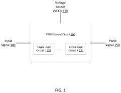
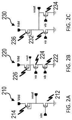
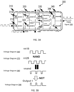
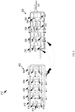
- Implementing logic circuitry using only n-type HEMTs to generate PWM signals with minimal to no power loss, utilizing a combination of enhancement mode (E-HEMTs) and depletion mode (D-HEMTs) in series to control duty cycles without the need for additional components like sawtooth generators, level shifters, or comparators.
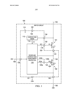
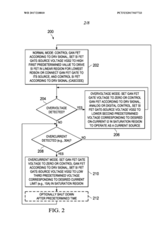
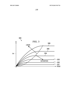
Overvoltage protection and short-circuit withstanding for gallium nitride devices
PatentWO2017218810A1
Innovation
- A driver and current source circuit are integrated with GaN transistors to detect overvoltage and overcurrent conditions, allowing controlled current sinking and cascode configuration to prevent damage, using a low voltage silicon transistor as a current source, either monolithically or in a dual-die configuration, to provide overvoltage and short-circuit protection.
Thermal Management Solutions for GaN PFC Circuits
Thermal management represents a critical challenge in GaN-based Power Factor Correction (PFC) circuits due to the high switching frequencies and power densities these devices enable. While GaN HEMTs offer superior performance compared to silicon alternatives, they generate significant heat that must be effectively dissipated to maintain reliability and performance.
Advanced thermal interface materials (TIMs) have emerged as essential components in GaN PFC thermal management strategies. These materials, including metal-based TIMs, phase change materials, and graphene-enhanced compounds, provide thermal conductivity values exceeding 10 W/m·K, significantly reducing the thermal resistance between GaN devices and heat sinks.
Innovative heat sink designs specifically optimized for GaN applications incorporate micro-channel structures and advanced fin geometries that maximize surface area while minimizing airflow resistance. Computational fluid dynamics simulations have demonstrated that these optimized designs can reduce junction temperatures by 15-20°C compared to conventional heat sinks when operating at equivalent power levels.
Active cooling solutions, including high-efficiency fans and liquid cooling systems, are increasingly being integrated into GaN PFC designs for high-power applications. Recent developments in two-phase cooling technologies, such as vapor chambers and thermosyphons, have shown particular promise, offering thermal resistance values below 0.1°C/W in compact form factors suitable for power electronics.
Thermal spreading techniques address the challenge of hot spots in GaN devices by distributing heat more evenly across larger areas. Embedded heat pipes and copper inlays within PCB designs have demonstrated up to 30% improvement in thermal spreading compared to standard FR-4 boards.
System-level thermal design approaches consider the entire PFC circuit as an integrated thermal system. This holistic methodology incorporates strategic component placement, optimized airflow paths, and thermal isolation of temperature-sensitive components from GaN devices. Thermal simulation tools have become essential in this process, enabling accurate prediction of thermal performance before physical prototyping.
Emerging technologies such as diamond heat spreaders and direct liquid cooling of semiconductor dies show significant potential for next-generation GaN PFC circuits. These advanced solutions may enable further increases in power density while maintaining acceptable operating temperatures, potentially supporting switching frequencies exceeding 5 MHz in practical applications.
Reliability and Lifetime Assessment of GaN HEMTs in PFC Applications
The reliability and lifetime assessment of GaN HEMTs in PFC applications represents a critical consideration for widespread commercial adoption. These devices operate under high-stress conditions in power factor correction circuits, including high switching frequencies, elevated temperatures, and substantial voltage swings that can accelerate degradation mechanisms.
Field reliability data indicates that GaN HEMTs demonstrate promising durability, with leading manufacturers reporting failure rates below 1 FIT (failures in time) under typical PFC operating conditions. However, these statistics require careful interpretation as they often represent accelerated testing rather than decades of field deployment experience available for silicon devices.
Several key degradation mechanisms affect GaN HEMT reliability in PFC applications. Dynamic Ron degradation, where on-resistance increases after high-voltage stress, particularly impacts efficiency in PFC topologies. Gate reliability issues, including threshold voltage shifts and gate leakage current increases, can compromise switching performance over time. Additionally, thermal cycling in PFC applications with variable loads creates mechanical stress at material interfaces, potentially leading to delamination or bond wire fatigue.
Industry-standard reliability testing protocols have been adapted specifically for GaN devices in PFC circuits. These include JEDEC qualification tests with modifications to address GaN-specific failure modes, HTOL (High Temperature Operating Life) testing under switching conditions rather than static bias, and power cycling tests that simulate the thermal stresses of real-world PFC operation.
Manufacturers have implemented several design enhancements to improve long-term reliability. Field plate structures reduce peak electric fields at critical device regions, mitigating degradation mechanisms. Advanced passivation techniques minimize surface-related failures, while improved thermal management solutions address the concentrated heat generation characteristic of GaN devices.
Lifetime prediction models for GaN HEMTs in PFC applications continue to evolve. Current approaches combine physics-of-failure methodologies with statistical analysis of accelerated test data. These models suggest that properly designed GaN-based PFC circuits can achieve operational lifetimes exceeding 15 years under typical conditions, though this varies significantly based on specific implementation details and operating environments.
Unlock deeper insights with Patsnap Eureka Quick Research — get a full tech report to explore trends and direct your research. Try now!
Generate Your Research Report Instantly with AI Agent
Supercharge your innovation with Patsnap Eureka AI Agent Platform!