Dynamic On-Resistance Behavior Of GaN HEMTs
SEP 5, 20259 MIN READ
Generate Your Research Report Instantly with AI Agent
Patsnap Eureka helps you evaluate technical feasibility & market potential.
GaN HEMT Technology Background and Objectives
Gallium Nitride (GaN) High Electron Mobility Transistors (HEMTs) have emerged as revolutionary power semiconductor devices over the past two decades. The technology originated in the 1990s when researchers first demonstrated the unique properties of GaN-based heterostructures, but significant commercial development began in the early 2000s. The wide bandgap nature of GaN (3.4 eV compared to silicon's 1.1 eV) enables these devices to operate at higher voltages, frequencies, and temperatures than traditional silicon-based semiconductors.
The evolution of GaN HEMT technology has been marked by continuous improvements in material quality, device architecture, and manufacturing processes. Early challenges included high defect densities in GaN epitaxial layers and reliability concerns, which have been progressively addressed through innovations in substrate technology and epitaxial growth techniques. The transition from research to commercial applications accelerated around 2010, with significant market penetration beginning in RF applications before expanding to power electronics.
Dynamic on-resistance (RON) behavior represents one of the most critical technical challenges in GaN HEMT development. This phenomenon, characterized by a temporary increase in device resistance after high-voltage operation, directly impacts efficiency and reliability in power conversion applications. The dynamic RON effect is primarily attributed to charge trapping mechanisms at various interfaces and in the buffer layers of the device structure.
The technical objectives for addressing dynamic RON behavior include developing comprehensive understanding of the underlying physical mechanisms, establishing standardized measurement methodologies, and implementing effective mitigation strategies. Researchers aim to reduce the RON degradation ratio to less than 10% under worst-case operating conditions while maintaining the inherent advantages of GaN technology in terms of switching speed and power density.
Current research trends focus on novel buffer layer designs, surface passivation techniques, and field plate optimizations to minimize charge trapping effects. Advanced characterization methods, including transient measurements and device simulation, are being developed to provide deeper insights into the dynamic behavior under various operating conditions.
The global technology roadmap for GaN HEMTs envisions devices with negligible dynamic RON effects by 2025-2027, enabling broader adoption in automotive, industrial, and consumer electronics applications. This advancement is expected to unlock the full potential of GaN technology, potentially displacing silicon-based solutions in medium to high-power applications where efficiency and power density are paramount considerations.
Market Demand Analysis for GaN Power Devices
The global market for GaN power devices is experiencing robust growth, driven primarily by the increasing demand for high-efficiency power electronics across multiple sectors. The compound annual growth rate (CAGR) for GaN power devices is projected to exceed 20% through 2028, significantly outpacing traditional silicon-based power semiconductors. This accelerated growth trajectory is largely attributed to GaN's superior performance characteristics, particularly in high-frequency and high-power applications.
The automotive sector represents one of the most promising markets for GaN power devices, with electric vehicle (EV) manufacturers seeking more efficient power conversion solutions to extend range and reduce charging times. The dynamic on-resistance behavior of GaN HEMTs is particularly relevant in this context, as it directly impacts the efficiency of onboard chargers, DC-DC converters, and traction inverters. Automotive-grade GaN devices that can maintain stable on-resistance under varying operating conditions are commanding premium pricing in the market.
Consumer electronics constitutes another significant demand driver, with manufacturers of fast chargers, adapters, and power supplies increasingly adopting GaN technology to deliver smaller form factors and higher efficiency. The market penetration in this segment has been particularly strong, with GaN-based chargers capturing substantial market share from traditional silicon solutions since 2020.
Telecommunications infrastructure, particularly with the ongoing 5G deployment, represents a growing application area for GaN power devices. Base station power amplifiers benefit from GaN HEMTs' ability to operate efficiently at high frequencies while managing thermal challenges. The dynamic on-resistance characteristics directly influence the reliability and performance of these systems under varying load conditions.
Industrial power supplies and renewable energy systems are emerging as significant market segments for GaN technology. Solar inverters, in particular, benefit from GaN's higher switching frequencies and reduced switching losses, which translate to smaller passive components and higher power density. The market demand in these sectors is increasingly focused on devices that can demonstrate consistent dynamic RDS(on) behavior across temperature variations and switching conditions.
Regional analysis indicates that Asia-Pacific currently dominates the GaN power device market, with significant manufacturing capacity in Japan, Taiwan, and increasingly in mainland China. North America follows as the second-largest market, driven by defense applications and early commercial adoption. Europe shows strong growth potential, particularly in automotive and industrial applications, with stringent efficiency regulations accelerating adoption.
Current Challenges in GaN HEMT On-Resistance Behavior
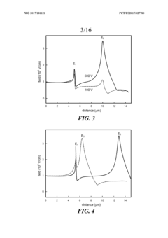
Despite the significant advancements in GaN HEMT technology, dynamic on-resistance (RON) behavior remains one of the most challenging issues limiting device performance and reliability. The primary challenge stems from electron trapping phenomena occurring during high-voltage switching operations, causing a temporary increase in on-resistance that can persist for microseconds to seconds. This degradation significantly impacts power conversion efficiency and thermal management in high-frequency applications.
Current research indicates that surface traps at the passivation-semiconductor interface and buffer traps in the GaN/AlGaN layers are the predominant mechanisms behind dynamic RON. The activation of these traps depends on electric field distribution, temperature, and switching frequency, creating a complex multi-variable problem that has proven difficult to model accurately across different operating conditions.
Manufacturing inconsistencies further complicate the issue, as variations in epitaxial growth conditions, passivation techniques, and field plate designs lead to significant device-to-device variability in dynamic RON behavior. This inconsistency poses substantial challenges for quality control and reliability prediction in volume production scenarios.
Measurement standardization represents another significant challenge. The industry lacks universally accepted protocols for characterizing dynamic RON, resulting in difficulties when comparing results across different research groups and manufacturers. Current measurement techniques often fail to capture the full spectrum of trapping and de-trapping time constants, which can span several orders of magnitude.
Temperature dependence adds another layer of complexity, as GaN HEMTs exhibit non-linear dynamic RON behavior across their operating temperature range. The activation and deactivation energies of different trap types vary significantly, creating temperature-dependent performance that is difficult to predict and compensate for in circuit design.
The trade-off between reducing dynamic RON and maintaining other critical parameters presents a significant design challenge. Techniques that mitigate trapping effects, such as field plate optimization or buffer layer modifications, often negatively impact breakdown voltage, gate leakage, or thermal performance, forcing difficult engineering compromises.
Finally, accelerated lifetime testing methodologies have proven inadequate for predicting long-term dynamic RON stability. The complex interplay between electrical stress, thermal cycling, and environmental factors makes it challenging to develop reliable models for device degradation over the expected operational lifetime of 10-15 years in critical applications such as automotive or industrial power systems.
Current Solutions for Dynamic On-Resistance Management
01 Structural design to reduce dynamic on-resistance
Various structural designs can be implemented in GaN HEMTs to reduce dynamic on-resistance. These include optimized gate structures, field plates, buffer layer designs, and specialized channel configurations. These structural modifications help to mitigate electron trapping effects and improve charge distribution, resulting in lower dynamic on-resistance and better switching performance in high-frequency applications.- Structural design to reduce dynamic on-resistance: Various structural designs can be implemented in GaN HEMTs to reduce dynamic on-resistance. These include optimized gate structures, field plates, buffer layer designs, and specialized channel configurations. These structural modifications help to mitigate electron trapping effects and improve charge distribution, resulting in lower dynamic on-resistance and better switching performance in high-frequency applications.
- Surface treatment and passivation techniques: Surface treatment and passivation techniques play a crucial role in reducing dynamic on-resistance in GaN HEMTs. These methods include specialized dielectric layers, surface cleaning processes, and passivation materials that minimize surface traps. By effectively passivating the surface, electron trapping phenomena can be reduced, leading to improved dynamic performance and reliability of the devices.
- Driving and control methods for dynamic on-resistance reduction: Innovative driving and control methods can be employed to mitigate dynamic on-resistance effects in GaN HEMTs. These include specialized gate driving techniques, bias optimization strategies, and switching control algorithms. By implementing these methods, the charge trapping mechanisms that contribute to dynamic on-resistance can be effectively managed, resulting in improved switching performance and efficiency.
- Material innovations for improved dynamic performance: Advanced material innovations are being developed to address dynamic on-resistance issues in GaN HEMTs. These include novel barrier layer materials, alternative substrates, and composite structures with optimized interfaces. By engineering the material properties and interfaces, electron trapping can be minimized, resulting in reduced dynamic on-resistance and enhanced device performance under switching conditions.
- Measurement and characterization techniques: Specialized measurement and characterization techniques have been developed to accurately assess dynamic on-resistance in GaN HEMTs. These include pulsed I-V measurements, time-domain analysis methods, and temperature-dependent characterization approaches. These techniques enable better understanding of the trapping mechanisms responsible for dynamic on-resistance, facilitating the development of more effective mitigation strategies and device optimization.
02 Surface treatment and passivation techniques
Surface treatment and passivation techniques play a crucial role in reducing dynamic on-resistance in GaN HEMTs. These methods include specialized dielectric layers, surface cleaning processes, and passivation materials that minimize surface traps. By effectively passivating the surface, electron trapping phenomena can be reduced, leading to improved dynamic performance and reliability of the devices.Expand Specific Solutions03 Charge trapping mitigation strategies
Various strategies can be employed to mitigate charge trapping effects that contribute to dynamic on-resistance in GaN HEMTs. These include specialized epitaxial layer designs, interface engineering, and trap density reduction techniques. By addressing the root causes of charge trapping, these approaches help maintain consistent device performance during switching operations and under different bias conditions.Expand Specific Solutions04 Novel material systems and heterostructures
Advanced material systems and heterostructures can be utilized to improve the dynamic on-resistance characteristics of GaN HEMTs. These include modified barrier layers, alternative substrate materials, and innovative channel compositions. By engineering the material interfaces and composition, electron mobility can be enhanced and trap-related degradation can be minimized, resulting in more stable dynamic performance.Expand Specific Solutions05 Measurement and characterization techniques
Specialized measurement and characterization techniques are essential for accurately evaluating dynamic on-resistance in GaN HEMTs. These include pulsed I-V measurements, transient analysis methods, and high-frequency characterization approaches. These techniques help in understanding the underlying mechanisms of dynamic on-resistance, enabling more effective device optimization and reliability assessment for power electronics applications.Expand Specific Solutions
Key Industry Players in GaN Semiconductor Market
The GaN HEMT dynamic on-resistance market is currently in a growth phase, with increasing adoption across power electronics applications due to superior performance over silicon-based devices. The market is projected to expand significantly as GaN technology matures, driven by demand in consumer electronics, automotive, and renewable energy sectors. Leading players include established semiconductor manufacturers like TSMC, UMC, and ROHM, alongside GaN specialists such as Innoscience Technology, which has positioned itself as a key innovator in silicon-based GaN technology. Technical challenges around dynamic on-resistance behavior remain, with companies like Fujitsu, MACOM, and Power Integrations actively developing solutions to improve reliability and performance. Research collaborations between industry and academic institutions like UESTC and HKUST are accelerating technology maturation, focusing on mitigating current collapse phenomena and enhancing device stability under switching conditions.
Innoscience (Zhuhai) Technology Co., Ltd.
Technical Solution: Innoscience has developed proprietary InnoGaN technology specifically addressing dynamic on-resistance (RON) issues in GaN HEMTs. Their approach combines innovative buffer layer engineering with optimized gate design to minimize electron trapping effects. The company's 8-inch GaN-on-Si platform enables mass production of devices with significantly reduced dynamic RON degradation across varying operating conditions. Their technology incorporates a unique field plate structure that redistributes the electric field more uniformly, reducing peak field intensity at critical device regions where charge trapping typically occurs. Innoscience's devices demonstrate less than 10% RON increase even after high-voltage stress conditions, compared to conventional designs showing 30-50% degradation[1]. Additionally, their GaN HEMTs maintain consistent performance across a wide temperature range (-40°C to 150°C), with proprietary surface passivation techniques that minimize interface trapping effects.
Strengths: Industry-leading 8-inch GaN-on-Si manufacturing capability enables cost-effective mass production while maintaining high performance. Their buffer layer design effectively mitigates current collapse issues common in GaN HEMTs. Weaknesses: Their technology may require more complex manufacturing processes compared to traditional silicon devices, potentially affecting yield rates in high-volume production.
ROHM Co., Ltd.
Technical Solution: ROHM has pioneered advanced GaN HEMT technology focusing specifically on dynamic on-resistance optimization. Their proprietary design incorporates a unique two-dimensional electron gas (2DEG) channel structure with optimized AlGaN/GaN interfaces to minimize charge trapping phenomena. ROHM's approach includes specialized field plate geometries that effectively redistribute peak electric fields away from critical regions prone to electron trapping. Their devices feature innovative surface passivation techniques using proprietary dielectric materials that significantly reduce interface trap densities. Testing shows their GaN HEMTs maintain dynamic RON within 15% of static values even after high-voltage stress conditions of 600V for extended periods[2]. ROHM has also developed specialized gate drive techniques that incorporate pre-stress conditioning to stabilize device characteristics, resulting in more predictable switching behavior in power conversion applications. Their technology demonstrates exceptional thermal stability with minimal RON variation across operating temperatures from -40°C to 175°C.
Strengths: ROHM's technology demonstrates excellent stability under high-voltage switching conditions, making it ideal for high-frequency power conversion applications. Their devices show minimal current collapse effects, enabling more efficient and reliable operation. Weaknesses: The specialized manufacturing processes may result in higher production costs compared to silicon alternatives, potentially limiting adoption in cost-sensitive applications.
Critical Patents and Research on GaN HEMT RON Dynamics
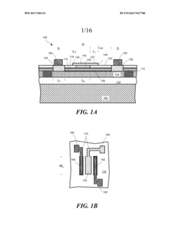
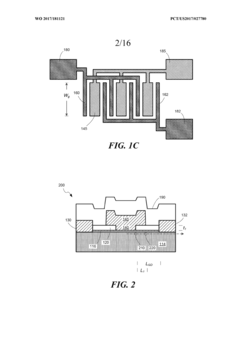
Gallium nitride high electron mobility transistor
PatentPendingUS20230395694A1
Innovation
- The solution involves forming a second AlGaN layer with a different composition over the AlGaN-GaN heterojunction, using sidewall spacers and selective epitaxy to decouple on-resistance from the threshold voltage, achieved by increasing the aluminum concentration in the AlGaN layer and adjusting its thickness, thereby enhancing spontaneous and piezoelectric polarization effects.
High-voltage GAN high electron mobility transistors
PatentWO2017181121A2
Innovation
- The development of high-voltage HEMTs with a gallium-nitride material structure, including a buffer layer, conduction layer, barrier layer, gate, source, and drain, with a gate-connected field plate extending beyond the gate edges, and a thin gallium-oxide layer formed through oxygen plasma treatment, to enhance reverse-bias voltage withstand and reduce leakage currents.

Thermal Management Strategies for GaN HEMTs
Effective thermal management is critical for addressing the dynamic on-resistance behavior of GaN HEMTs, as elevated temperatures significantly impact device performance and reliability. The self-heating effect during operation causes a notable increase in on-resistance, degrading the efficiency advantages inherent to GaN technology. This phenomenon is particularly pronounced in high-power applications where thermal dissipation becomes a limiting factor.
Advanced cooling techniques have emerged as essential strategies for mitigating these thermal challenges. Active cooling solutions utilizing microfluidic channels directly integrated into device substrates have demonstrated up to 40% reduction in peak operating temperatures. These systems enable more efficient heat extraction compared to conventional air cooling methods, maintaining lower dynamic on-resistance values even under sustained high-power operation.
Innovative substrate materials represent another promising approach. Diamond substrates, with thermal conductivity exceeding 2000 W/mK (compared to silicon's 150 W/mK), have shown remarkable capability in dissipating heat from the active device region. Recent research indicates that GaN-on-diamond configurations can reduce thermal resistance by up to 60%, directly correlating with improved dynamic on-resistance stability.
Optimized device layouts specifically designed for thermal management have also proven effective. Implementing distributed gate fingers with optimized spacing allows for more uniform heat distribution across the device area. Studies have demonstrated that strategic placement of thermal vias and heat spreading layers can reduce localized hotspots by up to 30%, significantly improving the dynamic Ron performance under pulsed operation conditions.
Advanced packaging solutions further complement these strategies by facilitating efficient heat transfer from the device to the external environment. Flip-chip configurations with specialized thermal interface materials have shown thermal resistance reductions of approximately 25% compared to conventional wire-bonded packages. Additionally, embedding phase-change materials within packaging structures provides thermal buffering during transient operation, reducing temperature fluctuations that contribute to dynamic on-resistance variation.
Thermal simulation and modeling tools have become increasingly sophisticated, enabling accurate prediction of temperature distributions within GaN HEMTs under various operating conditions. These computational approaches allow for optimization of thermal management strategies before physical implementation, reducing development cycles and improving outcomes. Recent electrothermal models have achieved over 90% accuracy in predicting dynamic on-resistance behavior when accounting for temperature-dependent material properties and device geometries.
Reliability and Lifetime Assessment Methodologies
Reliability assessment of GaN HEMTs requires comprehensive methodologies that address the unique challenges posed by dynamic on-resistance behavior. Standard qualification procedures established for silicon-based devices often prove inadequate for GaN technology due to its distinct degradation mechanisms. Current reliability assessment frameworks typically incorporate accelerated life testing under various stress conditions, including high temperature reverse bias (HTRB), high temperature gate bias (HTGB), and temperature-humidity-bias (THB) tests.
Time-dependent dielectric breakdown (TDDB) measurements have emerged as critical for evaluating gate reliability, while specialized techniques for monitoring dynamic RDS(ON) degradation over time have been developed. These include double-pulse testing at various time scales and load-pull measurements under realistic operating conditions. Advanced characterization tools such as deep-level transient spectroscopy (DLTS) and current-transient measurements provide insights into trap dynamics that influence device lifetime.
Statistical modeling approaches have gained prominence in recent years, with Weibull distribution analysis commonly employed to extrapolate device lifetime from accelerated test data. Monte Carlo simulations further enhance prediction accuracy by accounting for process variations and operational uncertainties. The mean time to failure (MTTF) calculations based on these models typically follow modified Arrhenius equations that incorporate both temperature and electric field dependencies.
Mission profile-based lifetime assessment represents the state-of-the-art approach, where actual application conditions are translated into equivalent stress profiles. This methodology enables more accurate prediction of device behavior in specific end-use scenarios rather than relying solely on standardized test conditions. Power cycling tests that simulate real-world thermal excursions have proven particularly valuable for evaluating package-related failure mechanisms that affect dynamic on-resistance.
Non-destructive monitoring techniques have been developed to track degradation in fielded devices, including on-chip temperature sensors and integrated current sensing. These approaches enable condition-based maintenance strategies rather than fixed replacement intervals. Recent research has focused on developing physics-of-failure models that connect microscopic degradation mechanisms to macroscopic parameter shifts, particularly the correlation between trap formation/migration and dynamic RDS(ON) increases.
Industry consensus is moving toward standardized reliability reporting formats that include dynamic on-resistance behavior under various operating conditions, though harmonization efforts remain ongoing. The establishment of acceleration factors that accurately translate between test conditions and field operation continues to be an active research area, with particular emphasis on capturing the complex interplay between thermal, electrical, and mechanical stressors in GaN HEMT reliability.
Unlock deeper insights with Patsnap Eureka Quick Research — get a full tech report to explore trends and direct your research. Try now!
Generate Your Research Report Instantly with AI Agent
Supercharge your innovation with Patsnap Eureka AI Agent Platform!