Paralleling GaN HEMTs: Challenges And Solutions
SEP 5, 20259 MIN READ
Generate Your Research Report Instantly with AI Agent
PatSnap Eureka helps you evaluate technical feasibility & market potential.
GaN HEMT Paralleling Background and Objectives
Gallium Nitride High Electron Mobility Transistors (GaN HEMTs) have emerged as revolutionary power semiconductor devices over the past two decades, offering superior performance characteristics compared to traditional silicon-based technologies. The evolution of GaN technology began in the early 1990s with fundamental research into wide bandgap semiconductors, progressing through significant milestones including the first demonstration of AlGaN/GaN heterostructures in 1993 and commercial availability beginning in the mid-2000s.
The technological trajectory of GaN HEMTs has been characterized by continuous improvements in material quality, device architecture, and manufacturing processes. Early challenges included high defect densities, limited substrate availability, and reliability concerns. However, persistent research efforts have yielded substantial advancements in epitaxial growth techniques, device passivation, and field management strategies, enabling today's high-performance GaN devices.
Paralleling GaN HEMTs represents a critical advancement in the technology's evolution, aimed at overcoming the inherent current handling limitations of individual devices. While single GaN HEMTs offer exceptional power density, applications requiring higher absolute power levels necessitate multiple devices operating in parallel configurations. This approach enables scaling of current capability while maintaining the fundamental advantages of GaN technology.
The primary objectives of GaN HEMT paralleling technology development include achieving uniform current distribution among parallel devices, maintaining switching synchronicity, managing thermal interactions, and ensuring stable operation under various operating conditions. These objectives are driven by the growing demand for higher power density, higher efficiency power conversion systems across multiple industries including automotive, renewable energy, data centers, and telecommunications infrastructure.
Current technical goals in this domain focus on optimizing interconnect designs to minimize parasitic inductances, developing advanced gate driving schemes for synchronized switching, implementing effective thermal management solutions, and creating robust protection mechanisms against potential device failures. Additionally, there is significant emphasis on developing standardized design methodologies and modeling approaches that accurately predict the behavior of paralleled GaN HEMT structures.
The evolution of GaN HEMT paralleling techniques is expected to enable new generations of power conversion systems with unprecedented performance metrics, including power densities exceeding 10 kW/L, efficiencies above 99%, and switching frequencies in the megahertz range. These advancements align with broader industry trends toward electrification, miniaturization, and improved energy efficiency across multiple application domains.
Market Demand Analysis for Parallel GaN HEMTs
The global market for Gallium Nitride (GaN) power devices is experiencing robust growth, driven primarily by the increasing demand for high-frequency, high-power applications across multiple industries. The parallel configuration of GaN High Electron Mobility Transistors (HEMTs) represents a significant segment within this market, as it addresses the power scaling limitations of individual devices.
Market research indicates that the overall GaN power device market is projected to grow at a compound annual growth rate of approximately 30% through 2026, with parallel GaN HEMT configurations becoming increasingly important in this expansion. This growth is primarily fueled by the superior performance characteristics of GaN technology compared to traditional silicon-based solutions, including higher breakdown voltage, faster switching speeds, and improved thermal performance.
The telecommunications sector represents one of the largest market segments for parallel GaN HEMTs, particularly in 5G infrastructure deployment where high-power, high-efficiency RF amplifiers are essential. Base station manufacturers are increasingly adopting parallel GaN HEMT configurations to achieve the power levels required for extended coverage while maintaining efficiency.
In the automotive sector, the transition toward electric vehicles (EVs) has created substantial demand for advanced power electronics. Parallel GaN HEMTs are gaining traction in onboard chargers and DC-DC converters, where their higher efficiency translates directly into extended vehicle range. Industry analysts note that automotive applications for GaN power devices are growing at nearly 40% annually, with parallel configurations becoming standard in higher-power applications.
Data center power supplies represent another significant market opportunity. As energy efficiency becomes a critical metric for data center operations, the superior performance of parallel GaN HEMT solutions in high-power density applications is driving adoption. The reduced cooling requirements and smaller form factors enabled by GaN technology align perfectly with the industry's push toward more compact and efficient facilities.
Consumer electronics manufacturers are also exploring parallel GaN HEMT implementations for fast-charging solutions. The market for high-power chargers (>100W) is expanding rapidly, with parallel GaN configurations enabling smaller form factors while delivering the required power levels.
Industrial power conversion represents a growing application area, with parallel GaN HEMTs being integrated into motor drives, industrial power supplies, and renewable energy inverters. The improved efficiency and reliability of these systems directly translate to operational cost savings, driving market demand despite higher initial component costs.
Defense and aerospace applications, while smaller in volume, represent high-value opportunities for parallel GaN HEMT technology. These sectors prioritize performance and reliability over cost considerations, making them ideal early adopters for advanced parallel configuration techniques and technologies.
Technical Challenges in GaN HEMT Paralleling
Gallium Nitride High Electron Mobility Transistors (GaN HEMTs) have emerged as revolutionary power devices due to their superior properties compared to silicon-based counterparts. However, paralleling these devices to achieve higher current handling capabilities presents significant technical challenges that must be addressed for successful implementation in high-power applications.
The fundamental challenge in GaN HEMT paralleling stems from device parameter mismatch. Even minor variations in threshold voltage, transconductance, and on-resistance between parallel devices can lead to current imbalance, resulting in thermal runaway and premature device failure. These variations originate from manufacturing process inconsistencies and inherent material property fluctuations in the GaN epitaxial layers.
Thermal management represents another critical challenge. GaN HEMTs generate substantial heat during operation, and when multiple devices are placed in close proximity, thermal coupling effects become pronounced. The resulting temperature gradients across parallel devices exacerbate parameter mismatch, creating a positive feedback loop that further destabilizes current sharing. This challenge is particularly acute in high-frequency applications where power density is exceptionally high.
Dynamic switching behavior discrepancies constitute a third major obstacle. GaN HEMTs exhibit extremely fast switching speeds with transition times in nanoseconds. When paralleled, even slight differences in gate drive paths, parasitic inductances, or device capacitances can cause significant switching timing variations. This leads to uneven stress distribution during switching transients, potentially triggering avalanche breakdown in devices that switch earlier than others.
Layout and packaging constraints further complicate GaN HEMT paralleling. The physical arrangement of devices must minimize parasitic inductances while maintaining thermal isolation. Traditional packaging technologies often fail to meet these contradictory requirements, necessitating novel approaches to interconnection and heat dissipation.
Gate drive design presents unique challenges for paralleled GaN HEMTs. Unlike silicon devices, GaN HEMTs have narrower gate voltage margins and are more sensitive to gate overvoltage and ringing. Ensuring synchronized and clean gate signals across multiple devices requires sophisticated driver circuits with precise timing control and impedance matching.
Parasitic oscillations represent a particularly insidious problem in paralleled GaN systems. The combination of high switching speeds and layout inductances can create resonant circuits that trigger high-frequency oscillations. These oscillations increase electromagnetic interference (EMI) and can cause device instability or failure if not properly suppressed through careful design of gate resistors, layout optimization, and filtering techniques.
Current Paralleling Solutions for GaN HEMTs
01 Parallel connection techniques for GaN HEMTs
Various techniques for connecting GaN HEMTs in parallel to increase power handling capability while maintaining efficiency. These methods include specific gate connection designs, balanced current distribution approaches, and thermal management considerations to ensure uniform operation across multiple devices. Parallel configurations help overcome individual device power limitations while maintaining the high-frequency performance advantages of GaN technology.- Parallel connection techniques for GaN HEMTs: Various techniques for connecting GaN HEMTs in parallel to increase power handling capability while maintaining efficiency. These methods include specific gate connection designs, synchronized switching mechanisms, and balanced current distribution approaches that help overcome the challenges of paralleling high-speed switching devices. The parallel configuration allows for higher current capacity and reduced on-resistance compared to single devices.
- Thermal management in paralleled GaN HEMTs: Thermal management solutions specifically designed for paralleled GaN HEMT structures to address heat dissipation challenges. These include specialized substrate materials, heat spreading techniques, and thermal interface optimizations that help maintain device reliability and performance under high-power operation. Effective thermal management is critical when multiple GaN HEMTs are operated in parallel due to increased power density.
- Layout and packaging innovations for paralleled GaN HEMTs: Novel layout and packaging approaches for paralleled GaN HEMTs that minimize parasitic inductances and capacitances. These innovations include optimized die placement, advanced interconnect technologies, and integrated packaging solutions that improve switching performance and reduce electromagnetic interference. The physical arrangement of paralleled devices significantly impacts overall system performance and reliability.
- Gate drive optimization for paralleled GaN HEMTs: Specialized gate drive circuits and methodologies designed for paralleled GaN HEMTs to ensure synchronized switching and balanced current sharing. These include matched gate resistors, isolated drive circuits, and advanced control algorithms that compensate for device parameter variations. Proper gate drive design is essential for preventing oscillations and ensuring stable operation in paralleled configurations.
- Device matching and current balancing techniques: Methods for selecting and matching GaN HEMTs for parallel operation to ensure balanced current distribution and prevent device overstress. These techniques include parameter screening, active current balancing circuits, and compensation networks that minimize the effects of device-to-device variations. Proper device matching is critical for maximizing the performance and reliability of paralleled GaN HEMT configurations.
02 Thermal management in paralleled GaN HEMTs
Solutions addressing thermal challenges in paralleled GaN HEMT structures. These include specialized heat dissipation structures, substrate materials with enhanced thermal conductivity, and layout designs that optimize heat distribution. Effective thermal management is critical for maintaining reliability and performance consistency across paralleled devices, preventing thermal runaway and ensuring balanced operation under high-power conditions.Expand Specific Solutions03 Gate drive optimization for paralleled GaN HEMTs
Specialized gate drive circuits and methodologies designed specifically for paralleled GaN HEMT configurations. These include synchronized driving techniques, impedance matching networks, and compensation circuits that account for parasitic elements. Optimized gate drive designs ensure uniform switching behavior across multiple devices, reducing switching losses and preventing oscillations that can occur in high-frequency parallel operations.Expand Specific Solutions04 Device matching and layout techniques
Methods for selecting and arranging GaN HEMTs in parallel configurations to ensure balanced operation. These include device parameter matching procedures, symmetrical layout designs, and interconnection techniques that minimize parasitic differences. Proper device matching and layout are essential for current sharing, preventing individual device overstress, and maintaining overall system reliability in high-power applications.Expand Specific Solutions05 Novel substrate and packaging solutions
Advanced substrate materials and packaging technologies specifically designed for paralleled GaN HEMT applications. These include integrated cooling solutions, low-inductance interconnect structures, and novel die-attach methods that enhance thermal and electrical performance. These innovations address the unique challenges of high-frequency, high-power operation in paralleled configurations, enabling more compact and efficient power systems.Expand Specific Solutions
Key Industry Players in GaN HEMT Development
The GaN HEMT paralleling technology market is currently in a growth phase, with increasing adoption in power electronics and RF applications. The market is expanding rapidly, projected to reach significant scale due to GaN's superior performance over silicon. Technologically, paralleling GaN HEMTs faces challenges in thermal management, current sharing, and parasitic oscillations. Leading players like Wolfspeed, Infineon, and GaN Systems have developed advanced solutions, while research institutions such as South China University of Technology and UESTC are contributing breakthrough innovations. Companies including Huawei, NXP, and STMicroelectronics are integrating these technologies into commercial applications. The ecosystem shows a collaborative approach between semiconductor manufacturers, academic institutions, and end-users to overcome technical barriers and accelerate market adoption.
Wolfspeed, Inc.
Technical Solution: Wolfspeed has developed advanced paralleling techniques for GaN HEMTs that focus on thermal management and current sharing optimization. Their approach incorporates specialized gate driving circuits with precise timing control to minimize switching transient imbalances between parallel devices. The company's solution includes custom-designed interconnect structures that equalize parasitic inductances and resistances, ensuring balanced current distribution across multiple GaN HEMTs. Wolfspeed's technology also features integrated temperature sensors and active feedback control systems that monitor and adjust individual device performance in real-time, preventing thermal runaway conditions. Their paralleling architecture has demonstrated the ability to maintain current sharing within 5% deviation across devices even under high-frequency switching conditions exceeding 1 MHz.
Strengths: Industry-leading SiC and GaN expertise with vertical integration from substrate to packaged device; proprietary gate driving technology minimizes switching losses. Weaknesses: Higher cost structure compared to silicon-based alternatives; requires sophisticated thermal management systems for high-power applications.
STMicroelectronics International NV
Technical Solution: STMicroelectronics has developed an integrated solution for GaN HEMT paralleling challenges through their PowerGaN technology platform. Their approach combines optimized device design with innovative packaging and control techniques. ST's solution features matched GaN HEMT devices with tightly controlled parameter spreads, reducing inherent current sharing imbalances. Their technology incorporates specialized gate driver circuits with independently adjustable slew rates and propagation delays, enabling synchronized switching of parallel devices. ST has implemented a unique thermal management architecture that includes embedded temperature sensors and thermal vias strategically placed to equalize heat distribution. Their paralleling technology also addresses electromagnetic interference challenges through optimized power loop layouts that minimize common-mode noise generation. The company has demonstrated successful parallel operation of up to 6 GaN HEMTs in high-power applications, achieving current balance within 10% deviation while maintaining switching speeds above 100 V/ns.
Strengths: Vertically integrated manufacturing capabilities from wafer to module; extensive automotive qualification experience brings reliability expertise to GaN paralleling. Weaknesses: More conservative approach to GaN implementation compared to pure-play GaN companies; paralleling solutions require sophisticated control systems that increase overall system cost.
Critical Patents and Innovations in GaN Paralleling
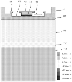
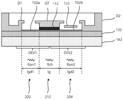
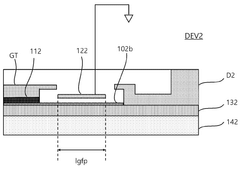
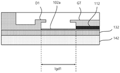
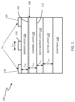
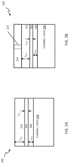
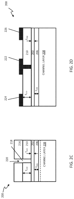
High electron mobility transistor and manufacturing method thereof
PatentWO2024258219A1
Innovation
- The solution involves tailoring the two-dimensional electron gas (2DEG) regions of the first and second drain terminals in GaN HEMTs by using barrier layers with different physical properties, such as varying Al mole fractions and doping concentrations, to optimize performance for voltage blocking and switching functions, and reducing device spacing for improved packaging density.
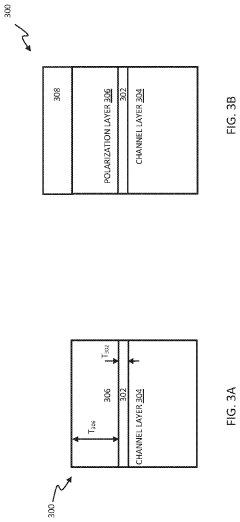
HIGH ELECTRON MOBILITY TRANSISTORS (HEMTS) INCLUDING A YTTRIUM (Y) AND ALUMINUM NITRIDE (AlN) (YAlN) ALLOY LAYER
PatentActiveUS20230223467A1
Innovation
- Incorporating a lattice-matched yttrium aluminum nitride (YAlN) alloy as a back-barrier layer in HEMTs, which has a wider bandgap than the gallium nitride channel layer, preventing secondary 2DEG formation and reducing thermal resistance, and can be used as an etch stop layer to improve electron confinement and gate control.
Thermal Management Strategies for Parallel GaN Devices
Thermal management represents a critical challenge in the parallel operation of GaN HEMTs due to their high power density and the thermal sensitivity of these devices. When multiple GaN HEMTs are connected in parallel to increase current handling capability, uneven temperature distribution can lead to current imbalance, thermal runaway, and ultimately device failure.
Advanced thermal management strategies begin with optimized package design. Diamond-based substrates with thermal conductivity exceeding 1500 W/mK offer superior heat dissipation compared to traditional silicon carbide substrates (370 W/mK). Recent developments in composite substrates combining copper with diamond particles have demonstrated a 40% improvement in thermal performance while maintaining cost-effectiveness for commercial applications.
Active cooling solutions have evolved significantly for parallel GaN implementations. Microfluidic cooling channels integrated directly into device packaging can remove heat fluxes exceeding 1000 W/cm², substantially outperforming conventional forced-air cooling methods. Two-phase cooling systems utilizing refrigerants in closed-loop configurations have demonstrated the ability to maintain temperature gradients below 5°C across parallel-connected devices, ensuring more uniform current distribution.
Thermal interface materials (TIMs) play a crucial role in heat transfer from devices to heat sinks. Graphene-enhanced TIMs have emerged as particularly effective for GaN applications, offering thermal conductivity up to 25 W/mK compared to 5-8 W/mK for conventional materials. These advanced TIMs reduce thermal resistance at interfaces by up to 60%, significantly improving overall thermal performance.
Dynamic thermal management through intelligent control systems represents another frontier in parallel GaN operation. Real-time temperature monitoring using integrated sensors allows for adaptive control of gate drive signals to balance current distribution among parallel devices. Research indicates that implementing temperature-compensated gate drive can reduce thermal variation by up to 70% among parallel-connected GaN HEMTs under high-load conditions.
Simulation-driven design approaches have become essential for optimizing thermal management in complex parallel configurations. Multi-physics modeling tools that simultaneously account for electrical, thermal, and mechanical interactions enable designers to predict hotspots and optimize layout geometries before physical prototyping. These simulation capabilities have reduced thermal design iterations by approximately 40% while improving thermal performance by 25-30% in recent commercial implementations.
Reliability and Lifetime Assessment of Paralleled GaN HEMTs
The reliability and lifetime assessment of paralleled GaN HEMTs represents a critical area of investigation for power electronics applications. When multiple GaN HEMTs are connected in parallel to increase current handling capability, their reliability characteristics become more complex than those of single devices. This complexity stems from the interaction between paralleled devices and the potential for uneven stress distribution.
Assessment methodologies for paralleled GaN HEMTs must account for both individual device degradation mechanisms and system-level interactions. Accelerated life testing under various operational conditions provides valuable data on potential failure modes specific to parallel configurations. These tests typically involve subjecting devices to elevated temperatures, higher switching frequencies, and increased voltage stress to induce accelerated aging.
Time-dependent dielectric breakdown (TDDB) emerges as a significant reliability concern in paralleled structures. The uneven distribution of electric fields across multiple devices can accelerate dielectric degradation in certain devices within the parallel arrangement. This phenomenon requires specialized testing protocols that monitor individual device performance within the parallel configuration.
Dynamic current sharing represents another critical reliability factor. As devices age at different rates, their electrical characteristics diverge, leading to current imbalance that further accelerates degradation. Advanced monitoring techniques using high-speed thermal imaging and electrical parameter extraction help identify early signs of current sharing degradation before catastrophic failure occurs.
Thermal management significantly impacts the lifetime of paralleled GaN HEMTs. Uneven temperature distribution across paralleled devices can create thermal hotspots that accelerate localized degradation. Studies indicate that a 10°C increase in junction temperature can reduce device lifetime by approximately 50%, making thermal design a crucial aspect of reliability engineering for paralleled configurations.
Statistical lifetime prediction models have been developed specifically for paralleled GaN structures. These models incorporate Monte Carlo simulations to account for device-to-device variations and their impact on overall system reliability. The Weibull distribution has proven particularly effective for modeling the failure rate distribution of paralleled GaN HEMTs under various operational conditions.
Field reliability data suggests that paralleled GaN HEMTs can achieve operational lifetimes exceeding 10 years when properly designed with adequate derating factors and thermal management. However, this requires comprehensive reliability testing during development and implementation of condition monitoring systems during operation to detect early signs of performance degradation.
Unlock deeper insights with PatSnap Eureka Quick Research — get a full tech report to explore trends and direct your research. Try now!
Generate Your Research Report Instantly with AI Agent
Supercharge your innovation with PatSnap Eureka AI Agent Platform!