What Are The Packaging Constraints In GaN HEMT Applications?
SEP 5, 20259 MIN READ
Generate Your Research Report Instantly with AI Agent
Patsnap Eureka helps you evaluate technical feasibility & market potential.
GaN HEMT Packaging Evolution and Objectives
Gallium Nitride High Electron Mobility Transistors (GaN HEMTs) have evolved significantly since their inception in the early 1990s. The packaging technology for these devices has undergone substantial transformation to address the unique characteristics of GaN, particularly its high power density, high operating frequency, and thermal management requirements. Initially, GaN HEMTs were packaged using modified versions of existing silicon-based packaging solutions, which limited their performance potential.
The evolution of GaN HEMT packaging can be traced through several distinct phases. The first generation utilized ceramic-based packages with gold metallization, offering improved thermal performance compared to traditional plastic packages but still falling short of GaN's full capabilities. The second generation introduced advanced thermal management solutions, incorporating copper-tungsten heat spreaders and diamond-based materials to enhance heat dissipation.
Current state-of-the-art packaging employs sophisticated multi-layer structures with optimized thermal interfaces, reduced parasitic inductances, and enhanced electrical performance. These packages often integrate advanced cooling solutions directly into the package design, such as microfluidic channels or embedded heat pipes, to manage the extreme thermal loads generated by GaN devices operating at high power densities.
The primary objective of modern GaN HEMT packaging is to maximize the inherent advantages of the technology while mitigating its challenges. This includes enabling operation at higher frequencies (beyond 100 GHz for some applications), managing increased power densities (>40 W/mm), and ensuring reliability under extreme operating conditions. Packaging solutions must simultaneously address thermal management, electrical performance, mechanical robustness, and cost-effectiveness.
Future packaging evolution aims to further reduce parasitic elements, particularly inductance and capacitance, which become increasingly critical at millimeter-wave frequencies. Integration of multiple functions within a single package, including passive components and other semiconductor technologies, represents another key objective to enable more compact and efficient RF systems.
The trend toward heterogeneous integration is particularly relevant for GaN HEMT packaging, with objectives focused on combining GaN with silicon, SiC, or other semiconductor materials in a single package to leverage the advantages of each technology. This approach requires novel interconnect solutions and careful management of thermal expansion mismatches between different materials.
Environmental considerations are also shaping packaging objectives, with increasing emphasis on lead-free solutions and recyclable materials that comply with global regulations while maintaining the performance advantages of GaN technology. The ultimate goal is to develop packaging solutions that allow GaN HEMTs to reach their theoretical performance limits while ensuring reliability, manufacturability, and cost-effectiveness for widespread commercial adoption.
Market Demand Analysis for GaN HEMT Solutions
The global market for GaN HEMT (High Electron Mobility Transistor) solutions has witnessed substantial growth in recent years, driven primarily by increasing demand for high-power and high-frequency applications. The market value for GaN power devices reached approximately $900 million in 2022 and is projected to grow at a CAGR of 18-20% through 2028, with packaging solutions representing a significant portion of this market.
The telecommunications sector remains the largest consumer of GaN HEMT technology, particularly with the ongoing global deployment of 5G infrastructure. Base stations require high-efficiency RF power amplifiers where GaN HEMTs excel, creating sustained demand for advanced packaging solutions that can handle thermal management challenges while maintaining signal integrity at millimeter-wave frequencies.
Defense and aerospace applications constitute another major market segment, valued at roughly $300 million annually. These applications demand ruggedized packaging capable of withstanding extreme environmental conditions while maintaining reliability. The need for radar systems with higher resolution and longer range is pushing the requirements for GaN HEMT packages that can support higher power densities without compromising performance.
The automotive sector represents the fastest-growing market for GaN HEMT solutions, particularly in electric vehicle (EV) applications. The EV charging infrastructure market alone is expected to grow at 25-30% annually, creating significant demand for GaN-based power conversion systems. These applications require packaging solutions that can withstand automotive qualification standards while delivering superior thermal performance and reliability.
Consumer electronics manufacturers are increasingly adopting GaN technology for fast chargers and power adapters, with market penetration accelerating as costs decrease. This segment demands ultra-compact packaging solutions that can handle the thermal challenges of high-power density applications while meeting strict consumer safety requirements and cost targets.
Industrial power systems represent another significant market opportunity, with growing demand for more efficient motor drives, power supplies, and renewable energy inverters. These applications require packaging solutions that can handle high voltages and currents while providing excellent thermal management and long-term reliability in harsh operating environments.
The market analysis reveals a clear trend toward integration, with customers increasingly demanding complete power modules rather than discrete components. This shift is driving innovation in packaging technologies that can accommodate multiple GaN devices alongside silicon-based control and protection circuitry, creating new opportunities for packaging solution providers who can address these complex integration challenges.
Current Packaging Limitations and Technical Challenges
GaN HEMT technology faces significant packaging constraints that limit its full potential in high-frequency, high-power applications. The primary challenge stems from the thermal management requirements, as GaN devices generate substantial heat during operation. Current packaging solutions struggle to efficiently dissipate this heat, leading to performance degradation and reliability issues. The thermal conductivity of conventional packaging materials (typically around 150-220 W/mK) falls short of what is optimal for GaN HEMTs, which ideally require materials with thermal conductivity exceeding 1000 W/mK.
Electrical parasitic effects represent another major constraint in GaN HEMT packaging. The high switching frequencies (often exceeding 100 MHz) characteristic of GaN devices make them particularly susceptible to parasitic inductances and capacitances introduced by packaging elements. These parasitics can significantly degrade device performance, limiting switching speeds and increasing power losses. Current packaging technologies typically introduce parasitic inductances of 0.2-1 nH, which becomes problematic at GaN's operating frequencies.
Size and form factor limitations also present challenges, particularly in applications requiring high power density. The need to incorporate effective thermal management solutions often conflicts with miniaturization goals, creating a fundamental design trade-off. This is especially problematic in aerospace, automotive, and portable electronics applications where space constraints are severe.
Material compatibility issues further complicate GaN HEMT packaging. The coefficient of thermal expansion (CTE) mismatch between GaN (5.6 ppm/K) and common packaging materials can lead to mechanical stress during thermal cycling, potentially causing delamination, cracking, or bond wire failures. This mismatch becomes more pronounced as operating temperatures increase, limiting the reliability of GaN devices in high-temperature applications.
Current hermetic packaging solutions, while effective for environmental protection, add significant cost and complexity to GaN HEMT devices. The hermetic sealing process often requires high temperatures that can stress the GaN die and surrounding components. Additionally, these packages typically increase the overall device footprint, contradicting the trend toward higher power density.
The integration of gate drivers and protection circuits presents another packaging challenge. These components are essential for proper GaN HEMT operation but require careful placement to minimize parasitic effects. Current packaging approaches often necessitate separate components, increasing system complexity and reducing overall reliability.
Manufacturing scalability remains problematic, with current GaN packaging techniques involving multiple specialized processes that are difficult to standardize and scale. This contributes to higher production costs and limits widespread adoption of GaN technology across various application domains.
Current Packaging Solutions and Approaches
01 Thermal management solutions for GaN HEMT packages
Effective thermal management is critical for GaN HEMT packages due to the high power density and heat generation during operation. Various solutions include advanced heat sinks, thermal interface materials, and innovative package designs that facilitate efficient heat dissipation. These approaches help maintain optimal device performance and reliability by preventing thermal runaway and degradation of the semiconductor material.- Thermal management solutions for GaN HEMT packages: Effective thermal management is critical for GaN HEMT packages due to the high power density and heat generation during operation. Various solutions include advanced heat sinks, thermal interface materials, and innovative package designs that facilitate efficient heat dissipation. These approaches help maintain optimal operating temperatures, prevent thermal runaway, and ensure long-term reliability of the device while maximizing performance.
- Package materials and structures for high-frequency operation: Specialized package materials and structures are essential for GaN HEMT devices operating at high frequencies. These include low-loss dielectric materials, optimized lead frames, and carefully designed signal paths to minimize parasitic effects. The package structure must maintain signal integrity while providing adequate protection from environmental factors, allowing the GaN HEMT to achieve its full high-frequency potential.
- Integration techniques for multi-chip modules: Advanced integration techniques enable the combination of GaN HEMTs with other semiconductor devices in multi-chip modules. These approaches include heterogeneous integration, 3D packaging, and system-in-package solutions that optimize the overall system performance. Such integration must address challenges related to thermal expansion mismatches, electrical interconnections, and maintaining the performance advantages of GaN technology.
- Reliability enhancement methods for harsh environments: GaN HEMT packages for harsh environment applications require specialized reliability enhancement methods. These include hermetic sealing techniques, robust interconnect designs, and protective coatings that shield against moisture, chemicals, and mechanical stress. Such packaging solutions ensure the long-term stability and performance of GaN HEMTs in automotive, aerospace, and industrial applications where environmental conditions are demanding.
- RF performance optimization through package design: Package design significantly impacts the RF performance of GaN HEMTs. Optimization techniques include minimizing bond wire lengths, implementing air cavity packages, utilizing low-loss materials, and carefully designing ground paths. These approaches reduce parasitic inductances and capacitances that can degrade high-frequency performance. Advanced RF packaging solutions enable GaN HEMTs to achieve their full potential in terms of power output, efficiency, and bandwidth.
02 Package materials and structures for high-frequency operation
Specialized package materials and structures are essential for GaN HEMT devices operating at high frequencies. These include low-loss dielectric materials, optimized lead frames, and carefully designed signal paths to minimize parasitic inductance and capacitance. The package structure must maintain signal integrity while providing adequate protection from environmental factors and mechanical stress.Expand Specific Solutions03 Integration with passive components and circuit elements
GaN HEMT packages often require integration with passive components and other circuit elements to optimize performance. This integration presents challenges in terms of space constraints, electromagnetic interference, and thermal considerations. Advanced packaging techniques such as system-in-package (SiP) and embedded passive components are employed to address these challenges while maintaining the high-frequency performance of the GaN HEMT devices.Expand Specific Solutions04 Reliability and environmental protection considerations
GaN HEMT packages must be designed to ensure long-term reliability and protection against environmental factors. This includes moisture resistance, protection against electrostatic discharge, and mechanical robustness. Hermetic sealing, specialized encapsulation materials, and stress-relieving structures are employed to enhance reliability while maintaining the electrical and thermal performance of the device.Expand Specific Solutions05 Size and form factor optimization for specific applications
The size and form factor of GaN HEMT packages must be optimized for specific applications, such as mobile communications, radar systems, or power electronics. This optimization involves trade-offs between thermal performance, electrical characteristics, and mechanical constraints. Advanced packaging technologies, including chip-scale packaging and wafer-level packaging, are employed to achieve the desired balance between performance and size constraints.Expand Specific Solutions
Key Industry Players in GaN HEMT Packaging
The GaN HEMT market is currently in a growth phase, with increasing adoption across power electronics, RF applications, and telecommunications. The market size is expanding rapidly, projected to reach significant value as demand for high-frequency, high-power devices grows. From a technical maturity perspective, the packaging of GaN HEMTs presents unique challenges due to thermal management requirements and parasitic effects. Leading players like Innoscience Technology, Qorvo, and STMicroelectronics have made substantial progress in addressing these constraints through advanced packaging solutions. Chinese institutions including Xidian University and UESTC are contributing significant research, while companies such as Huawei Digital Power and Fujitsu are developing commercial applications. The competitive landscape shows a mix of established semiconductor manufacturers and specialized GaN-focused startups working to overcome the thermal dissipation, electrical performance, and reliability challenges inherent to GaN HEMT packaging.
Fujitsu Ltd.
Technical Solution: Fujitsu has developed sophisticated packaging solutions for GaN HEMT applications, particularly focused on RF and power electronics markets. Their approach utilizes advanced direct copper bonding (DCB) substrates with optimized thermal vias that reduce junction-to-case thermal resistance to approximately 0.3°C/W for high-power devices. Fujitsu's packaging technology incorporates specialized molding compounds with thermal conductivity exceeding 5 W/m·K, significantly higher than standard epoxy materials. For RF applications, they've pioneered air-cavity packages with controlled impedance transitions that maintain signal integrity up to 40GHz. Their GaN HEMT packages feature integrated temperature sensors within 0.1mm of the active die area, enabling precise thermal monitoring and protection. Fujitsu has also developed specialized die-attach materials that can withstand over 10,000 thermal cycles between -40°C and 150°C without degradation, critical for automotive applications. Their recent innovations include packages with integrated electromagnetic interference (EMI) shielding that reduces emissions by over 20dB compared to standard packages.
Strengths: Superior thermal management capabilities; excellent high-frequency performance preservation; robust reliability under thermal cycling. Weaknesses: Higher manufacturing costs compared to conventional packaging; larger minimum size requirements for certain high-power applications; complex assembly process requiring specialized equipment.
Innoscience (Zhuhai) Technology Co., Ltd.
Technical Solution: Innoscience has developed innovative packaging solutions for GaN HEMT applications that address thermal management challenges through their proprietary InnoGaN technology. Their approach utilizes advanced thermal interface materials and optimized package designs that reduce junction-to-case thermal resistance to below 0.5°C/W for high-power devices. The company employs dual-side cooling techniques where heat is extracted from both the top and bottom of the die, significantly improving thermal performance in high-power density applications. Innoscience has also pioneered ultra-low profile packaging with heights under 0.5mm, enabling integration into space-constrained consumer electronics. Their packaging technology incorporates specialized EMI shielding structures directly into the package design to mitigate electromagnetic interference issues common in high-frequency GaN operations. Additionally, they've developed proprietary die-attach materials that maintain reliability under high-temperature cycling conditions typical in automotive and industrial applications.
Strengths: Industry-leading thermal performance enabling higher power density; ultra-thin package profiles suitable for mobile applications; integrated EMI shielding reducing system complexity. Weaknesses: Higher manufacturing costs compared to traditional packaging; requires specialized assembly equipment; thermal expansion mismatch challenges with certain substrate materials.
Critical Patents and Innovations in GaN HEMT Packaging
Gallium nitride high electron mobility transistor and method for manufacturing the same
PatentPendingUS20250273534A1
Innovation
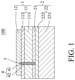
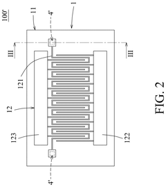
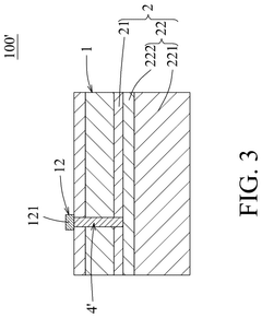
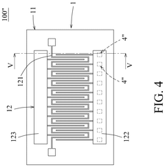
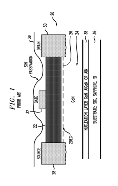
- A GaN HEMT design incorporating a heat dissipation structure with a molybdenum substrate and conductive channels to dissipate heat efficiently, while guiding electrodes to the backside for traditional packaging, reducing parasitic inductance.
Gallium nitride superjunction devices
PatentInactiveUS20130240951A1
Innovation
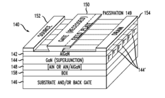
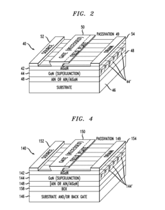
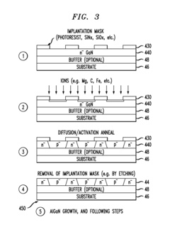
- Incorporating a doped gallium nitride superjunction layer with a plurality of p/n junctions between the substrate and a barrier layer, which suppresses breakdown by modifying the electric field distribution, allowing for higher breakdown voltages and enabling the use of low-cost Si substrates.
Thermal Management Strategies for GaN HEMT Packages
Thermal management represents a critical challenge in GaN HEMT packaging due to the high power density and operating temperatures these devices generate. Conventional packaging solutions often prove inadequate for effectively dissipating the substantial heat produced during operation, which can reach thermal densities exceeding 1 kW/mm². This limitation necessitates innovative thermal management strategies specifically tailored for GaN HEMT applications.
Direct substrate cooling techniques have emerged as a primary approach, where materials with superior thermal conductivity such as silicon carbide (SiC) and diamond are integrated directly into the package design. These materials offer thermal conductivity values of 120-490 W/mK for SiC and up to 2000 W/mK for diamond, significantly outperforming traditional silicon substrates (149 W/mK).
Advanced heat spreading technologies incorporate specialized thermal interface materials (TIMs) to enhance heat transfer between the die and package. Metal-based TIMs utilizing indium, gallium, or silver sintering have demonstrated thermal resistances below 0.1 K·cm²/W, representing a substantial improvement over conventional polymer-based solutions.
Microfluidic cooling channels integrated directly into GaN HEMT packages present another promising strategy. These microscale channels allow coolant circulation in close proximity to heat-generating regions, achieving cooling capacities of 1000 W/cm² or higher. Recent developments in this area include two-phase cooling systems that leverage the latent heat of vaporization to further enhance thermal performance.
Package-level thermal solutions incorporate advanced heat sink designs with optimized fin structures and vapor chambers. These designs can reduce thermal resistance by 30-40% compared to traditional extruded heat sinks. Additionally, embedded heat pipe technologies within the package substrate provide effective heat spreading with thermal conductivities exceeding 5000 W/mK along the axial direction.
Active cooling integration, including thermoelectric coolers and miniature liquid cooling systems, offers dynamic thermal management capabilities that can respond to varying operational demands. These systems can maintain junction temperatures within 10-15°C of ambient conditions even under high-power operation.
Emerging approaches include phase change materials (PCMs) embedded within package structures to absorb thermal energy during peak operation and release it during idle periods, effectively dampening thermal transients. Additionally, 3D packaging architectures with through-silicon vias (TSVs) and interposers facilitate more direct thermal paths from heat sources to cooling solutions, reducing overall thermal resistance by up to 50% compared to traditional wire-bonded packages.
Reliability and Qualification Standards for GaN Packaging
The reliability and qualification standards for GaN packaging represent a critical framework for ensuring the long-term performance and safety of GaN HEMT devices in various applications. These standards have evolved significantly over the past decade, transitioning from adapted silicon-based methodologies to GaN-specific protocols that address the unique thermal and electrical characteristics of these high-power devices.
Industry standards such as JEDEC JEP180 and AEC-Q101 have established baseline requirements for GaN device qualification, with particular emphasis on thermal cycling, high-temperature operating life (HTOL), and moisture sensitivity level (MSL) testing. These standards typically require devices to withstand 1000 hours of operation at maximum rated temperature and voltage while maintaining performance parameters within specified limits.
Thermal management qualification has become increasingly stringent, with standards now requiring comprehensive characterization of thermal resistance pathways and verification of package integrity under extreme thermal cycling conditions (-65°C to +150°C). This reflects the recognition that thermal dissipation represents one of the most significant challenges in GaN HEMT packaging reliability.
Electrical qualification standards have also evolved to address GaN-specific concerns, including dynamic Ron testing and gate reliability assessment. Current standards mandate rigorous evaluation of breakdown voltage stability and leakage current characteristics over extended operational periods, typically 2000+ hours under accelerated stress conditions.
Mechanical robustness testing has been enhanced to account for the unique material interfaces in GaN packages. Standards now specify more comprehensive die shear testing, wire bond pull strength requirements, and package warpage limitations to ensure reliability in automotive and industrial environments where mechanical stress is significant.
Radiation hardness qualification has emerged as a distinct requirement for aerospace and military applications, with standards defining specific testing protocols for total ionizing dose (TID) and single event effects (SEE) resistance. These standards typically require demonstration of stable operation after exposure to radiation levels appropriate for the intended application environment.
The qualification timeline for GaN packaging has been compressed in recent years, with accelerated testing methodologies gaining acceptance. However, industry consensus maintains that certain long-term reliability aspects still require extended evaluation periods, particularly for mission-critical applications where field failures cannot be tolerated.
Unlock deeper insights with Patsnap Eureka Quick Research — get a full tech report to explore trends and direct your research. Try now!
Generate Your Research Report Instantly with AI Agent
Supercharge your innovation with Patsnap Eureka AI Agent Platform!
