Design Strategies For EMI Reduction In GaN HEMT Circuits
SEP 8, 202510 MIN READ
Generate Your Research Report Instantly with AI Agent
Patsnap Eureka helps you evaluate technical feasibility & market potential.
GaN HEMT EMI Challenges and Objectives
Gallium Nitride High Electron Mobility Transistors (GaN HEMTs) have emerged as revolutionary power semiconductor devices, offering superior performance characteristics compared to traditional silicon-based technologies. These devices exhibit higher breakdown voltage, faster switching speeds, and lower on-resistance, making them ideal candidates for high-frequency, high-power applications. However, these same advantages present significant electromagnetic interference (EMI) challenges that must be addressed for successful implementation in commercial and industrial systems.
The evolution of GaN HEMT technology has been marked by continuous improvements in material quality, device structure, and fabrication processes. Initially developed for military and aerospace applications, GaN HEMTs have gradually expanded into commercial sectors including telecommunications, automotive, and renewable energy systems. This transition has highlighted the critical need for effective EMI management strategies, as these applications often operate in electromagnetically sensitive environments.
The rapid switching capabilities of GaN HEMTs, while beneficial for efficiency, generate significant high-frequency noise components that can propagate throughout systems and interfere with nearby electronics. Switching speeds up to ten times faster than silicon devices create steeper voltage and current transitions (higher dv/dt and di/dt), resulting in broadband EMI extending into the hundreds of megahertz range.
Current technical trends indicate a push toward higher operating frequencies, increased power densities, and more compact system designs, all of which exacerbate EMI challenges. The industry is witnessing a convergence of power electronics and RF design principles to address these issues, with increasing emphasis on integrated approaches to EMI mitigation rather than traditional add-on filtering solutions.
The primary objective of EMI reduction strategies in GaN HEMT circuits is to maintain the performance advantages of these devices while minimizing electromagnetic emissions to comply with regulatory standards and ensure system reliability. This requires a multi-faceted approach encompassing device-level optimizations, circuit layout techniques, packaging innovations, and system-level considerations.
Specific technical goals include developing design methodologies that address the unique EMI signature of GaN HEMTs, creating predictive models for EMI generation and propagation, establishing best practices for PCB layout and component placement, and formulating integrated shielding and filtering strategies tailored to GaN-based systems.
Additionally, there is a growing need for standardized testing protocols and compliance frameworks specifically adapted to the high-frequency characteristics of GaN technology. The ultimate aim is to establish a comprehensive design ecosystem that enables engineers to fully leverage GaN HEMT capabilities while maintaining electromagnetic compatibility with surrounding systems and meeting increasingly stringent regulatory requirements.
Market Demand for Low-EMI GaN Power Solutions
The global market for GaN HEMT (High Electron Mobility Transistor) power solutions with low electromagnetic interference (EMI) characteristics is experiencing robust growth, driven by increasing demands across multiple industries. Power electronics systems utilizing GaN technology are becoming essential in applications where space constraints, efficiency, and electromagnetic compatibility are critical factors.
The automotive sector represents one of the largest market segments demanding low-EMI GaN solutions, particularly with the rapid expansion of electric vehicles (EVs). The compound annual growth rate for GaN power devices in automotive applications exceeds 30%, with particular emphasis on onboard chargers and DC-DC converters where EMI reduction is paramount for ensuring vehicle electronics reliability and compliance with stringent automotive standards.
Consumer electronics manufacturers are increasingly adopting GaN-based power adapters and chargers due to their smaller form factor and higher efficiency. Market research indicates that consumers are willing to pay premium prices for fast-charging solutions that don't interfere with other electronic devices, creating a significant value proposition for low-EMI GaN technology.
The telecommunications infrastructure sector presents another substantial market opportunity. As 5G networks continue to expand globally, base stations require compact, efficient power solutions that minimize electromagnetic interference with sensitive communication equipment. The density of these installations in urban environments makes EMI reduction a non-negotiable requirement rather than a mere feature.
Data center operators are similarly investing in GaN power solutions to address power density challenges while maintaining electromagnetic compatibility within increasingly crowded server environments. The total addressable market for low-EMI GaN solutions in data centers is growing at approximately 25% annually, driven by the need for more efficient power conversion with minimal interference.
Industrial automation systems represent another significant market segment where precision control systems require clean power with minimal electromagnetic noise. Manufacturing facilities are increasingly adopting GaN-based motor drives and power supplies specifically designed to reduce EMI that could otherwise compromise sensitive instrumentation and control systems.
Regulatory pressures are further accelerating market demand, with updated EMC (Electromagnetic Compatibility) standards becoming more stringent across regions. Companies are proactively seeking GaN solutions with superior EMI characteristics to future-proof their designs against evolving compliance requirements.
Market analysis reveals that customers are increasingly specifying EMI performance as a primary selection criterion for power solutions, rather than treating it as a secondary consideration. This shift represents a fundamental change in market dynamics, creating premium opportunities for GaN solutions with advanced EMI reduction strategies built into their design architecture.
Current EMI Mitigation Techniques and Limitations
Current EMI mitigation techniques for GaN HEMT circuits can be broadly categorized into layout design, packaging, filtering, and system-level approaches. Layout optimization techniques include minimizing loop areas, careful routing of high-speed signals, and implementing ground planes to reduce parasitic inductances. These methods have proven effective in conventional silicon-based circuits but face limitations when applied to GaN technology due to the higher switching speeds and steeper voltage transitions.
Signal filtering represents another widely adopted approach, with common-mode chokes and ferrite beads frequently employed to attenuate high-frequency noise. However, these components often introduce additional parasitic elements that can degrade the high-frequency performance advantages inherent to GaN technology. The trade-off between EMI suppression and maintaining the performance benefits of GaN becomes increasingly challenging as operating frequencies rise.
Shielding techniques, including metal enclosures and EMI-absorbing materials, provide substantial reduction in radiated emissions but add significant weight, volume, and thermal management complications. This approach contradicts the miniaturization advantages that GaN technology offers, creating a fundamental design conflict.
Spread spectrum clock generation (SSCG) has emerged as an effective technique to distribute EMI energy across a wider frequency band, thereby reducing peak emissions. While effective in many applications, SSCG introduces timing uncertainties that may be unacceptable in precision-timing applications where GaN circuits are increasingly deployed.
Soft-switching techniques aim to reduce EMI by controlling the voltage and current transition rates during switching events. Although these methods show promise, they often compromise the switching efficiency that makes GaN attractive in the first place, presenting a significant limitation.
Current gate driver designs for GaN HEMTs typically focus on optimizing switching speed but pay insufficient attention to EMI generation. Advanced gate driving techniques that balance switching performance with controlled slew rates remain underdeveloped, representing a critical gap in current mitigation strategies.
System-level approaches such as differential signaling and balanced power distribution have demonstrated effectiveness but require significant design complexity and board space. The implementation challenges intensify in high-density GaN applications where space constraints are already severe.
The fundamental limitation across all current mitigation techniques is their reactive nature—they attempt to suppress EMI after it has been generated rather than addressing the root causes within the GaN device physics and circuit topology. This reactive approach inevitably leads to performance compromises that undermine the inherent advantages of GaN technology.
State-of-the-Art EMI Suppression Circuit Designs
01 Shielding and packaging techniques for GaN HEMT circuits
Various shielding and packaging techniques can be employed to reduce electromagnetic interference (EMI) in GaN HEMT circuits. These include metal shields, specialized packaging materials, and electromagnetic shielding structures that can effectively contain and redirect electromagnetic radiation. Advanced packaging designs incorporate grounding structures and EMI-absorbing materials to minimize radiation leakage from high-frequency GaN HEMT devices, thereby reducing interference with nearby electronic components.- Shielding and packaging techniques for GaN HEMT circuits: Various shielding and packaging techniques can be employed to reduce electromagnetic interference (EMI) in GaN HEMT circuits. These include metal shields, specialized packaging materials, and encapsulation methods that contain electromagnetic emissions. Advanced packaging designs incorporate grounded metal layers and EMI-absorbing materials to prevent radiation from escaping the device, while maintaining thermal performance essential for high-power GaN operation.
- Layout optimization and circuit design techniques: Optimizing the layout of GaN HEMT circuits can significantly reduce EMI generation and propagation. This includes careful placement of components, minimizing loop areas in high-frequency paths, and implementing proper grounding schemes. Advanced circuit design techniques such as differential signaling, balanced transmission lines, and strategic placement of decoupling capacitors help mitigate EMI issues. These design approaches address EMI at the source by reducing parasitic inductances and capacitances that contribute to unwanted emissions.
- Integration of EMI filters and suppression components: Integrating specialized EMI filters and suppression components directly into GaN HEMT circuits provides effective EMI reduction. These include common-mode chokes, ferrite beads, and specialized capacitor arrangements designed to attenuate high-frequency noise. Advanced filter topologies can be tailored to address specific frequency bands where GaN HEMTs typically generate the most interference, offering targeted EMI suppression without compromising circuit performance.
- Substrate and material innovations for EMI reduction: Novel substrate materials and structures can inherently reduce EMI in GaN HEMT circuits. High-resistivity substrates, engineered composite materials, and specialized dielectric layers help contain electromagnetic fields within the device. Some approaches incorporate EMI-absorbing materials directly into the substrate or use advanced epitaxial techniques to create buffer layers that reduce parasitic emissions while maintaining the electrical performance of the GaN HEMT devices.
- Active EMI cancellation and compensation techniques: Active EMI cancellation techniques involve sensing electromagnetic emissions and generating opposing signals to neutralize them. These sophisticated approaches use feedback mechanisms to dynamically adjust cancellation signals based on operating conditions. Some implementations incorporate dedicated compensation circuits that predict and counteract EMI generation during switching events, which are particularly problematic in GaN HEMT circuits due to their fast switching speeds. These active methods can address EMI issues that passive techniques alone cannot effectively mitigate.
02 Layout optimization and circuit design techniques
Optimizing the layout and design of GaN HEMT circuits can significantly reduce EMI emissions. Techniques include careful routing of high-speed signal paths, minimizing loop areas in critical paths, and implementing differential signaling. Strategic placement of components and optimized trace geometries can reduce parasitic inductances and capacitances that contribute to EMI. Advanced circuit topologies specifically designed for GaN HEMTs can inherently produce lower electromagnetic emissions while maintaining high performance.Expand Specific Solutions03 Integration of filtering components and structures
Incorporating specialized filtering components and structures within GaN HEMT circuits can effectively suppress EMI. These include on-chip EMI filters, decoupling capacitors, ferrite beads, and common-mode chokes strategically placed to attenuate noise at specific frequencies. Advanced multi-stage filtering approaches can address both conducted and radiated emissions across broad frequency ranges, particularly important for the high switching speeds characteristic of GaN technology.Expand Specific Solutions04 Novel substrate and material solutions
Utilizing specialized substrate materials and novel semiconductor structures can inherently reduce EMI in GaN HEMT circuits. High-resistivity substrates, engineered buffer layers, and advanced epitaxial structures can minimize parasitic conduction paths that contribute to EMI. Composite materials with specific electromagnetic properties can be incorporated into the device structure to absorb or redirect electromagnetic radiation, thereby reducing overall emissions from the circuit.Expand Specific Solutions05 Gate drive and switching control optimization
Optimizing gate drive circuits and implementing advanced switching control techniques can significantly reduce EMI in GaN HEMT circuits. Controlled switching transitions with optimized slew rates can minimize high-frequency components that contribute to EMI. Adaptive gate driving schemes that respond to operating conditions can maintain efficiency while reducing electromagnetic emissions. Synchronization techniques for multiple devices and strategic dead-time management further minimize noise generation during switching events.Expand Specific Solutions
Leading Companies in GaN HEMT and EMI Mitigation
The EMI reduction in GaN HEMT circuits market is in a growth phase, with increasing adoption across telecommunications, defense, and automotive sectors. The market is projected to expand significantly as GaN technology matures, driven by demands for higher efficiency power electronics. Leading players include established semiconductor manufacturers like Taiwan Semiconductor Manufacturing Co., Infineon Technologies, and GlobalFoundries, alongside specialized GaN-focused companies such as Cambridge GaN Devices and Innoscience Technology. Academic institutions including Xidian University and University of Electronic Science & Technology of China are contributing significant research. The technology is advancing from early adoption to mainstream implementation, with companies focusing on addressing EMI challenges to unlock GaN's full potential in high-frequency applications.
Lockheed Martin Corp.
Technical Solution: Lockheed Martin has developed sophisticated EMI reduction strategies for GaN HEMT circuits focused on military and aerospace applications where electromagnetic compatibility is critical. Their approach combines advanced shielding techniques with specialized circuit topologies designed to contain and cancel electromagnetic emissions. Lockheed's designs implement differential power architectures with carefully balanced transmission lines to minimize common-mode emissions, particularly important in radar and communication systems. They've pioneered specialized enclosure designs with engineered apertures and gaskets that effectively contain high-frequency emissions while maintaining thermal performance. Their EMI reduction strategy includes custom-designed filtering networks that target specific frequency bands of concern in military systems, with particular attention to intermodulation products that can affect nearby sensitive receivers. Lockheed Martin has also developed advanced simulation capabilities that model both circuit behavior and electromagnetic field propagation to predict EMI characteristics before hardware implementation.
Strengths: Comprehensive approach addressing both circuit-level and system-level EMI concerns; solutions tested in extremely demanding electromagnetic environments; expertise in meeting stringent military EMC standards. Weaknesses: Solutions often optimized for performance over cost; approaches may be overengineered for commercial applications; technologies may have export restrictions due to defense applications.
United Monolithic Semiconductors SAS
Technical Solution: United Monolithic Semiconductors (UMS) has developed specialized EMI reduction techniques for GaN HEMT circuits focused primarily on RF and microwave applications. Their approach centers on monolithic integration of EMI mitigation structures directly within the GaN HEMT semiconductor process. UMS has pioneered on-chip filtering techniques including integrated capacitive and inductive elements strategically placed to suppress parasitic oscillations and reduce emissions at the source. Their designs implement specialized guard ring structures and substrate engineering to minimize substrate coupling effects that can propagate EMI through the system. UMS has developed advanced packaging solutions with optimized transitions between chip and package to maintain signal integrity while minimizing radiation. Their EMI reduction strategy includes specialized bias network designs that filter noise on power supply lines while maintaining stable operation under dynamic conditions. UMS has also implemented novel layout techniques that balance parasitic elements to create self-cancelling electromagnetic fields, reducing overall emissions without compromising RF performance.
Strengths: Highly integrated approach addressing EMI at the semiconductor level; solutions optimized for high-frequency operation; reduced dependence on external components for EMI suppression. Weaknesses: Limited to applications within UMS's process capabilities; less flexibility for customer-specific modifications; potentially higher cost for lower frequency applications where discrete solutions might suffice.
Critical Patents and Research in GaN EMI Control
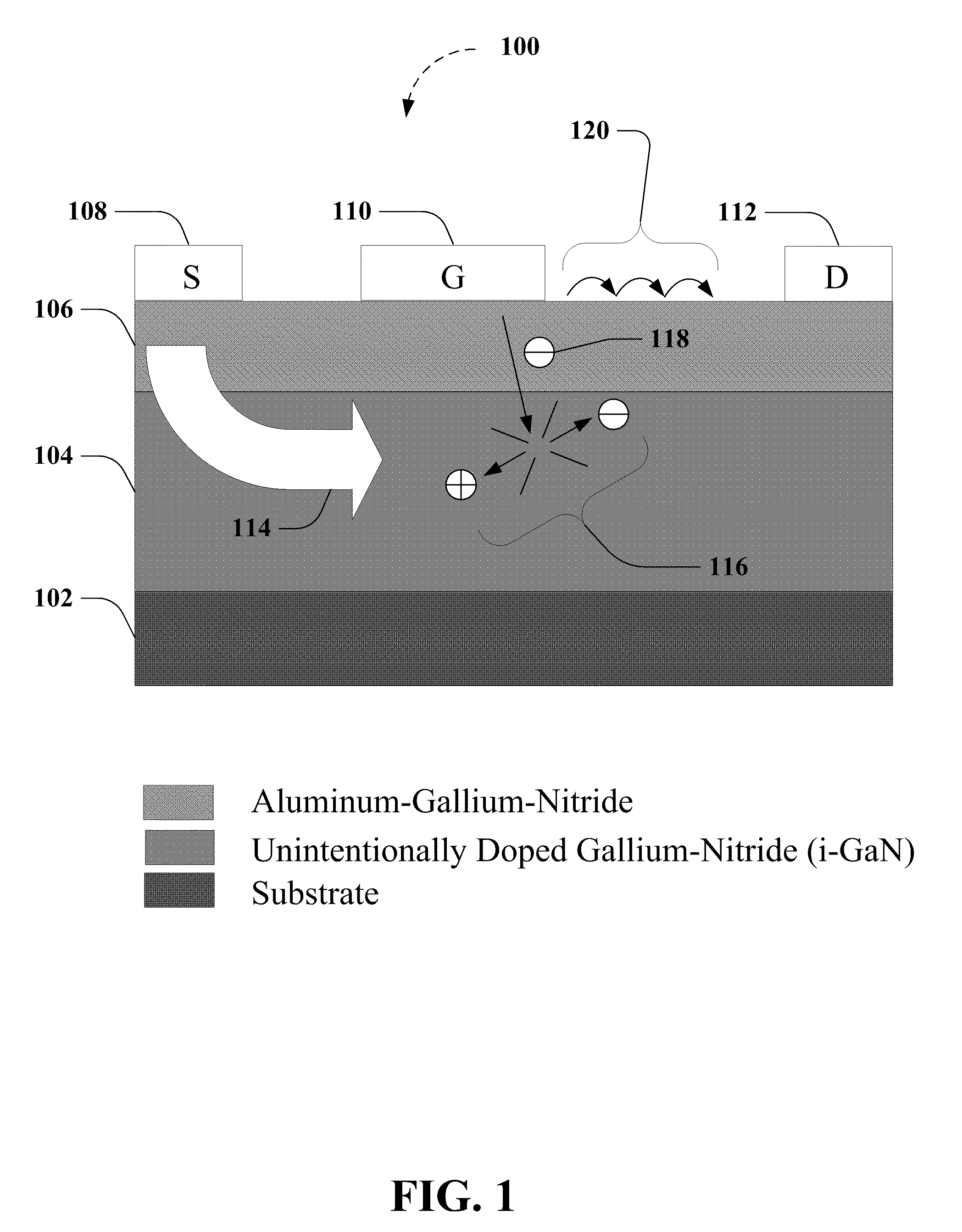
HEMT device and method of manufacturing the same
PatentWO2013176904A1
Innovation
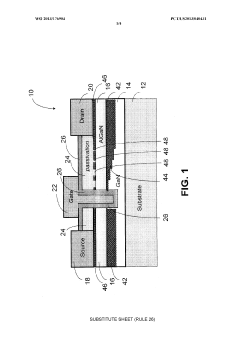
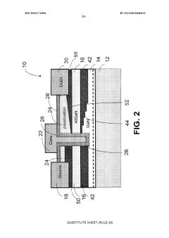
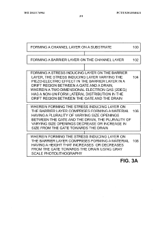
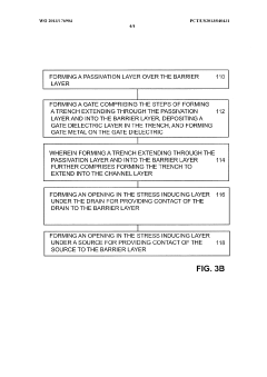
- A high electron mobility transistor (HEMT) with a non-uniform lateral two-dimensional electron gas (2DEG) profile is achieved by incorporating a stress-inducing layer with varying piezoelectric effect in the drift region between the gate and drain, using either varying size openings or height profiles to modulate the 2DEG density, thereby optimizing electric field distribution.
Aluminum gallium nitride/gallium nitride high electron mobility transistors
PatentInactiveUS20100084687A1
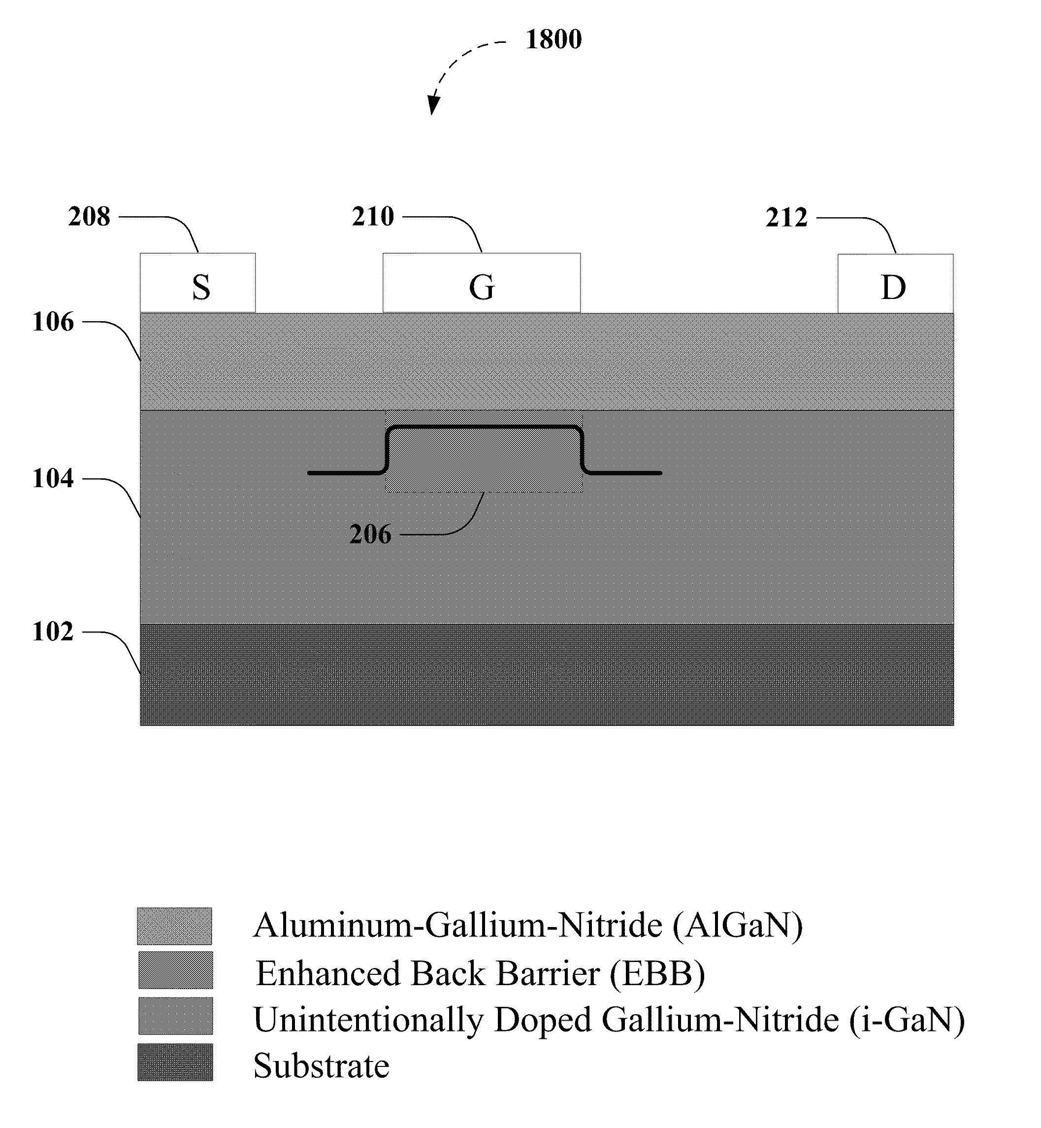
Innovation
- The implementation of fluorine ion implantation to create an enhanced back barrier in the GaN buffer layer, increasing the energy barrier at the 2DEG channel and reducing source current injection, thereby enhancing the off-state breakdown voltage.
Regulatory Compliance and EMC Standards
Compliance with electromagnetic compatibility (EMC) standards is a critical aspect of GaN HEMT circuit design, particularly as these high-frequency, high-power devices can generate significant electromagnetic interference (EMI). The regulatory landscape for EMC is complex and varies across different regions, with standards bodies such as the International Electrotechnical Commission (IEC), Federal Communications Commission (FCC), and European Telecommunications Standards Institute (ETSI) establishing specific requirements.
For GaN HEMT circuits, the most relevant EMC standards include IEC 61000 series, which addresses various aspects of electromagnetic compatibility, including emission limits, immunity requirements, and testing methodologies. Specifically, IEC 61000-4-3 for radiated RF immunity and IEC 61000-4-6 for conducted RF immunity are particularly important due to the high-frequency operation of GaN devices.
In the United States, FCC Part 15 regulations govern unintentional radiators, setting strict limits on conducted and radiated emissions across different frequency bands. GaN HEMT circuits, especially those operating at high switching frequencies, must be carefully designed to meet these requirements. Similarly, in Europe, the EN 55011/CISPR 11 standards classify equipment based on their industrial, scientific, and medical applications and establish corresponding emission limits.
Military and aerospace applications of GaN HEMT technology face even more stringent requirements under standards such as MIL-STD-461G, which specifies detailed EMI/EMC requirements for military equipment. These standards address both conducted and radiated emissions (CE and RE) as well as conducted and radiated susceptibility (CS and RS).
Compliance testing for GaN HEMT circuits typically involves pre-compliance testing during the design phase, followed by formal certification testing in accredited laboratories. Pre-compliance testing can identify potential issues early, allowing for design modifications before final certification. Testing methodologies include the use of anechoic chambers, GTEM cells, and specialized EMI receivers to measure emissions across specified frequency ranges.
Design strategies specifically targeting regulatory compliance include implementing proper PCB layout techniques such as controlled impedance traces, strategic component placement, and effective grounding schemes. Additionally, incorporating appropriate filtering components, shielding structures, and spread spectrum techniques can help meet emission requirements while maintaining circuit performance.
As GaN technology continues to evolve with higher frequencies and power densities, staying current with evolving EMC standards becomes increasingly important. Designers must consider compliance requirements from the earliest stages of the design process rather than as an afterthought, integrating EMC-aware design practices throughout the development cycle to ensure both performance and regulatory compliance.
Thermal Management Impact on EMI Performance
Thermal management in GaN HEMT circuits significantly impacts electromagnetic interference (EMI) performance, creating a complex interdependency that designers must carefully navigate. As operating temperatures increase in GaN devices, their electrical characteristics change, leading to shifts in switching behavior that can exacerbate EMI issues. Research indicates that junction temperature variations of just 20°C can alter switching speeds by up to 15%, directly affecting EMI spectral content.
The thermal gradient across GaN HEMT devices creates non-uniform switching patterns, particularly problematic in multi-device configurations where temperature differences between devices lead to timing mismatches. These mismatches generate additional high-frequency components in the EMI spectrum, often manifesting as broadband noise that is difficult to filter effectively.
Heat dissipation pathways in GaN circuits can inadvertently function as EMI propagation channels. Thermal vias, heat spreaders, and cooling structures, while necessary for temperature management, may create unintended antennas or coupling paths if not properly designed. Studies have shown that improper placement of thermal vias can increase radiated emissions by up to 6-8 dB in the 100-500 MHz range.
Advanced thermal management solutions offer dual benefits for EMI reduction. Techniques such as embedded cooling channels and phase-change materials not only stabilize device temperatures but also provide opportunities for EMI shielding integration. For instance, metal-based heat spreaders can be designed with specific geometries that simultaneously dissipate heat and attenuate electromagnetic radiation, particularly when connected to appropriate ground planes.
Temperature fluctuations affect the performance of EMI filtering components. Capacitors and ferrite materials used in EMI suppression exhibit temperature-dependent characteristics, with some ceramic capacitors losing more than 50% of their capacitance at elevated temperatures. This degradation reduces filter effectiveness precisely when switching transients may be most severe due to thermal effects on the GaN devices themselves.
Real-time thermal management systems that dynamically adjust switching parameters based on temperature monitoring have shown promise in maintaining consistent EMI profiles across varying operating conditions. Adaptive gate driving techniques that compensate for temperature-induced changes in device characteristics can maintain consistent switching edges, reducing the variability in EMI generation that typically occurs as systems heat up during operation.
Simulation tools that integrate both thermal and electromagnetic modeling capabilities are becoming essential for predicting these complex interactions. Combined electro-thermal-electromagnetic simulations enable designers to identify potential hotspots that might compromise EMI performance before physical prototyping, reducing development cycles and improving first-pass design success rates.
Unlock deeper insights with Patsnap Eureka Quick Research — get a full tech report to explore trends and direct your research. Try now!
Generate Your Research Report Instantly with AI Agent
Supercharge your innovation with Patsnap Eureka AI Agent Platform!