High-Voltage Applications Of GaN HEMT Devices
SEP 5, 20259 MIN READ
Generate Your Research Report Instantly with AI Agent
Patsnap Eureka helps you evaluate technical feasibility & market potential.
GaN HEMT Evolution and High-Voltage Goals
Gallium Nitride High Electron Mobility Transistors (GaN HEMTs) have undergone significant evolution since their inception in the early 1990s. Initially developed for RF applications due to their high electron mobility and saturation velocity, these devices have progressively expanded into power electronics domains. The fundamental structure of GaN HEMTs leverages the two-dimensional electron gas (2DEG) formed at the AlGaN/GaN heterojunction, which enables exceptional carrier transport properties without intentional doping.
The evolution trajectory of GaN HEMTs has been marked by several technological breakthroughs. Early devices suffered from current collapse phenomena and reliability issues that limited their high-voltage performance. The introduction of field plates in the mid-2000s represented a critical advancement, effectively redistributing the electric field and enhancing breakdown voltage capabilities. Subsequently, the development of enhancement-mode architectures through gate recess techniques, p-GaN gates, and hybrid approaches addressed the normally-on limitation of conventional HEMTs.
Material quality improvements have played a pivotal role in GaN HEMT evolution. The transition from sapphire to silicon carbide substrates, and later to silicon for cost reduction, has been accompanied by significant reductions in dislocation densities. Advanced epitaxial growth techniques have minimized buffer leakage currents, which is essential for high-voltage operation where vertical breakdown mechanisms become increasingly relevant.
The high-voltage goals for GaN HEMTs are driven by applications in electric vehicle charging infrastructure, renewable energy conversion, and industrial motor drives. These applications demand devices capable of blocking voltages exceeding 1200V while maintaining low on-resistance and high switching frequencies. The theoretical limit for GaN, determined by its critical electric field strength of approximately 3.3 MV/cm, suggests potential for devices operating beyond 5kV.
Current high-voltage GaN HEMT research focuses on several key objectives: optimizing buffer layer designs to suppress leakage currents, developing novel field management structures to enhance breakdown voltage, improving thermal management for higher power density, and enhancing reliability under high-voltage stress conditions. The vertical GaN architecture represents a paradigm shift, potentially offering superior high-voltage performance compared to lateral devices by better utilizing the material's intrinsic capabilities.
The roadmap for GaN HEMTs in high-voltage applications envisions devices with progressively increasing breakdown voltages, reduced specific on-resistance, and enhanced thermal performance. Industry targets include achieving 1700V-rated devices with competitive cost structures by 2025, and pushing toward 3kV-capable devices for medium-voltage applications by 2030, potentially disrupting the traditional silicon carbide and silicon IGBT domains.
Market Analysis for High-Voltage GaN Applications
The global market for high-voltage GaN applications is experiencing robust growth, driven primarily by the increasing demand for efficient power electronics across multiple sectors. Current market valuations place the high-voltage GaN device market at approximately 223 million USD in 2023, with projections indicating a compound annual growth rate (CAGR) of 35% through 2028, potentially reaching 1 billion USD by that time.
The automotive sector represents the largest and fastest-growing application segment for high-voltage GaN devices. Electric vehicle (EV) manufacturers are increasingly adopting GaN-based power electronics for onboard chargers, DC-DC converters, and traction inverters due to their superior efficiency and power density compared to silicon alternatives. This adoption is accelerating as EV production volumes increase globally, with particularly strong demand in China, Europe, and North America.
Industrial power supplies constitute the second-largest market segment, where high-voltage GaN devices are enabling more compact and efficient power conversion systems. The industrial sector values the reduced cooling requirements and smaller form factors that GaN technology enables, particularly in applications requiring 650V and above operating voltages.
Renewable energy systems, particularly solar inverters and wind power converters, represent another significant growth area. The higher switching frequencies possible with GaN devices allow for smaller passive components and improved efficiency in power conversion, directly translating to improved economics for renewable energy installations.
Data center power infrastructure is emerging as a promising application area, driven by the exponential growth in cloud computing and the corresponding need for more efficient power delivery systems. The energy savings potential of GaN-based power supplies is particularly attractive in this sector, where power consumption represents a major operational cost.
Regionally, Asia-Pacific dominates the market with approximately 45% share, followed by North America (30%) and Europe (20%). China's aggressive push toward electrification and renewable energy has created particularly strong demand for advanced power semiconductors in the region.
Market barriers include the relatively higher cost of GaN devices compared to silicon alternatives, though this gap is narrowing as production volumes increase. Additionally, concerns about long-term reliability in high-voltage applications and the need for specialized design expertise have slowed adoption in some conservative sectors like aerospace and medical equipment.
The competitive landscape features both established semiconductor manufacturers expanding into GaN and specialized GaN-focused startups. This dynamic is driving innovation while simultaneously helping to reduce costs through increased competition and production scale.
GaN HEMT Technology Status and Challenges
GaN HEMT technology has witnessed significant advancements globally, with major research centers in the United States, Europe, Japan, and increasingly China making substantial contributions. The current state-of-the-art GaN HEMTs for high-voltage applications can achieve breakdown voltages exceeding 1500V, with some laboratory demonstrations reaching up to 3000V. However, these impressive figures come with considerable challenges that limit widespread commercial adoption in high-voltage domains.
One primary technical challenge is the management of dynamic Ron, where the device's on-resistance increases after high-voltage stress, significantly degrading performance in switching applications. This phenomenon, attributed to charge trapping effects at the surface and buffer layers, remains incompletely understood despite extensive research efforts. Current mitigation strategies include optimized passivation layers and field plate structures, but a comprehensive solution remains elusive.
Another critical limitation is current collapse, where the maximum drain current decreases after high-voltage operation. This reliability concern directly impacts the device's power handling capability and switching performance in high-voltage circuits. The industry has made progress through improved epitaxial growth techniques and device architectures, but further optimization is required for high-voltage applications above 1200V.
Thermal management presents a significant challenge as GaN HEMTs operate at higher power densities than silicon or SiC devices. The thermal conductivity of GaN substrates and the thermal boundary resistance between layers create bottlenecks for heat dissipation. Advanced packaging solutions and substrate engineering are being explored, with diamond integration showing promise despite manufacturing complexities.
The lack of native GaN substrates at commercially viable costs forces most high-voltage GaN HEMTs to be grown on foreign substrates like silicon, sapphire, or SiC. This heteroepitaxial growth introduces defects and dislocations that compromise device performance and reliability. While SiC substrates offer superior thermal and lattice matching properties, their high cost limits mass-market adoption for high-voltage applications.
Gate reliability under high electric fields remains problematic, with gate leakage and dielectric breakdown limiting voltage handling capability. Research into novel gate dielectrics, including Al2O3, HfO2, and their multilayer combinations, shows promise but faces integration challenges with GaN surface chemistry.
Manufacturing scalability presents another hurdle, as high-voltage GaN HEMTs require precise control of epitaxial growth, device geometry, and process parameters. The industry is gradually transitioning from 6-inch to 8-inch wafer processing, though yield and uniformity issues persist, particularly for devices targeting operating voltages above 900V.
Current High-Voltage GaN HEMT Solutions
01 GaN HEMT Device Structures and Fabrication
Gallium Nitride High Electron Mobility Transistors (GaN HEMTs) have specific structural designs that enhance their performance characteristics. These devices typically include a GaN buffer layer, an AlGaN barrier layer, and specialized gate structures. The fabrication processes involve epitaxial growth techniques, gate formation methods, and surface treatments that significantly impact device performance. Advanced structural designs may incorporate field plates, passivation layers, and specialized channel engineering to optimize electron mobility and power handling capabilities.- GaN HEMT device structures and fabrication methods: Gallium Nitride High Electron Mobility Transistors (GaN HEMTs) have specific structural designs and fabrication techniques that enhance their performance. These include specialized layer structures, epitaxial growth methods, and device architecture optimizations. The fabrication process typically involves substrate preparation, epitaxial growth of GaN and AlGaN layers, gate formation, and metallization steps to create high-performance power devices with improved electron mobility and reduced on-resistance.
- Enhancement-mode GaN HEMT technologies: Enhancement-mode (normally-off) GaN HEMTs are critical for power applications requiring fail-safe operation. Various techniques are employed to achieve normally-off operation, including gate recess structures, p-GaN gates, fluorine plasma treatment, and cascode configurations. These approaches modify the threshold voltage to ensure the device remains off without applied gate voltage, while maintaining the high breakdown voltage and low on-resistance advantages of GaN technology.
- Thermal management and reliability solutions for GaN HEMTs: Thermal management is crucial for GaN HEMT reliability and performance. Advanced solutions include integrated heat spreaders, novel substrate materials with higher thermal conductivity, optimized device layouts for heat dissipation, and specialized packaging techniques. These approaches address the self-heating effects that can limit device performance and lifetime, particularly in high-power applications where thermal management directly impacts reliability and power handling capability.
- GaN HEMT for RF and power applications: GaN HEMTs are optimized differently for RF and power applications. For RF applications, devices feature field plates, air-bridge structures, and specialized passivation to maximize frequency response and power density for communications systems. For power applications, designs focus on breakdown voltage enhancement, current collapse mitigation, and switching performance optimization. These application-specific designs enable GaN HEMTs to excel in both high-frequency communications and efficient power conversion systems.
- Advanced materials and interfaces for GaN HEMTs: Novel materials and interface engineering techniques enhance GaN HEMT performance. These include alternative barrier layers (such as InAlN), novel cap layers, interface treatment methods, and advanced dielectrics for gate insulation. Buffer layer optimization techniques reduce leakage current and improve breakdown characteristics. These material innovations address key challenges in GaN technology including current collapse, dynamic on-resistance, and long-term reliability while pushing the performance boundaries of these devices.
02 Thermal Management Solutions for GaN HEMTs
Thermal management is critical for GaN HEMT devices due to their high power density operation. Various approaches have been developed to address heat dissipation challenges, including advanced substrate materials with high thermal conductivity, integrated heat spreaders, and novel packaging solutions. Thermal interface materials and optimized device layouts help to reduce thermal resistance and hot spots. Effective thermal management solutions significantly improve device reliability, performance, and operational lifetime under high-power conditions.Expand Specific Solutions03 Reliability Enhancement Techniques
Improving the reliability of GaN HEMT devices involves addressing various degradation mechanisms such as current collapse, gate leakage, and electron trapping. Techniques include specialized surface passivation, buffer layer optimization, and field management structures. Advanced reliability enhancement approaches incorporate trap density reduction methods, edge termination designs, and stress testing protocols. These techniques aim to extend device lifetime, maintain stable performance under various operating conditions, and improve resistance to electrical and thermal stress.Expand Specific Solutions04 RF and Power Electronics Applications
GaN HEMT devices are widely used in radio frequency (RF) and power electronics applications due to their superior high-frequency performance and power handling capabilities. In RF applications, these devices enable high-efficiency power amplifiers for telecommunications, radar systems, and satellite communications. For power electronics, GaN HEMTs offer advantages in switching speed, breakdown voltage, and power density, making them suitable for power converters, motor drives, and renewable energy systems. Specialized designs optimize these devices for specific frequency bands and power requirements.Expand Specific Solutions05 Integration and Packaging Technologies
Advanced integration and packaging technologies for GaN HEMT devices focus on optimizing electrical performance while ensuring reliable thermal and mechanical characteristics. These include flip-chip bonding, through-substrate vias, and heterogeneous integration with other semiconductor technologies. Novel packaging approaches address parasitic effects, thermal expansion mismatches, and electromagnetic interference concerns. Integration solutions enable compact multi-chip modules, system-in-package designs, and improved interconnect technologies that maintain the inherent performance advantages of GaN HEMT devices in complex system applications.Expand Specific Solutions
Leading GaN HEMT Manufacturers and Competitors
The high-voltage GaN HEMT device market is currently in a growth phase, with increasing adoption across power electronics applications. The global market size is expanding rapidly, projected to reach significant valuation as industries transition to more efficient power solutions. In terms of technical maturity, leading players like Wolfspeed, Fujitsu, and Taiwan Semiconductor Manufacturing Co. have achieved commercial-grade GaN HEMT technologies, while companies such as Huawei, QUALCOMM, and Northrop Grumman are advancing specialized applications. Research institutions including Xidian University and University of Electronic Science & Technology of China are contributing fundamental innovations. The competitive landscape features established semiconductor giants alongside specialized GaN-focused startups, with differentiation occurring through device performance metrics, reliability improvements, and manufacturing scalability for high-voltage applications.
Wolfspeed, Inc.
Technical Solution: Wolfspeed has pioneered advanced GaN HEMT technology specifically designed for high-voltage applications, focusing on their proprietary HD-GIT (Hybrid Drain-Gate Injection Transistor) architecture. This innovative design combines traditional HEMT structures with unique gate injection features that significantly improve breakdown voltage capabilities up to 1200V while maintaining low on-resistance characteristics. Their technology implements specialized field plate structures and buffer layer engineering to manage peak electric fields at critical device regions, enabling operation at higher voltages without compromising reliability. Wolfspeed's GaN-on-SiC platform provides superior thermal conductivity compared to GaN-on-Si alternatives, allowing their devices to handle higher power densities in demanding applications. Their manufacturing process incorporates advanced passivation techniques and edge termination structures that enhance device robustness against voltage transients and environmental stressors[1][3].
Strengths: Superior thermal management through SiC substrates enabling higher power density; excellent dynamic RDS(on) characteristics minimizing switching losses; industry-leading breakdown voltage ratings. Weaknesses: Higher manufacturing costs compared to silicon-based alternatives; requires specialized packaging solutions to fully utilize high-frequency capabilities; thermal expansion coefficient mismatch challenges in certain assembly processes.
Fujitsu Ltd.
Technical Solution: Fujitsu has developed sophisticated GaN HEMT technology optimized for high-voltage applications in telecommunications infrastructure and advanced radar systems. Their approach centers on proprietary "N-polar" GaN crystal orientation that provides inherent advantages for high-voltage operation by reducing surface-related electron trapping effects. Fujitsu's devices incorporate specialized field management structures including stepped field plates and optimized passivation layers that work synergistically to distribute electric fields more uniformly across the device structure. Their manufacturing process utilizes advanced MOCVD epitaxial growth techniques with precise in-situ monitoring to ensure exceptional material quality and interface control. Fujitsu has pioneered specialized surface treatment protocols that minimize interface states and associated charge trapping phenomena, significantly improving dynamic performance under high-voltage switching conditions. Their GaN HEMTs feature proprietary source-connected field plate structures that effectively reduce gate-drain capacitance while maintaining high breakdown voltage, enabling faster switching speeds in high-voltage applications[3][6].
Strengths: Exceptional RF performance at high voltages; superior reliability in harsh environmental conditions; advanced packaging solutions optimized for thermal management. Weaknesses: Higher manufacturing complexity increasing production costs; limited commercial availability outside specific market segments; requires specialized design considerations to fully utilize performance capabilities.
Key Patents in High-Voltage GaN Technology
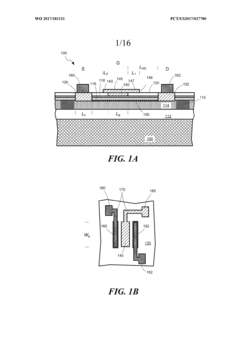
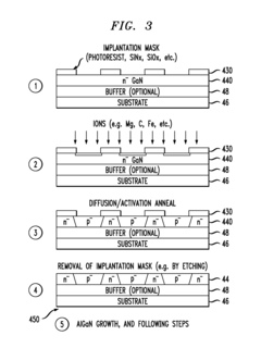
High-voltage GAN high electron mobility transistors
PatentWO2017181121A2
Innovation
- The development of high-voltage HEMTs with a gallium-nitride material structure, including a buffer layer, conduction layer, barrier layer, gate, source, and drain, with a gate-connected field plate extending beyond the gate edges, and a thin gallium-oxide layer formed through oxygen plasma treatment, to enhance reverse-bias voltage withstand and reduce leakage currents.

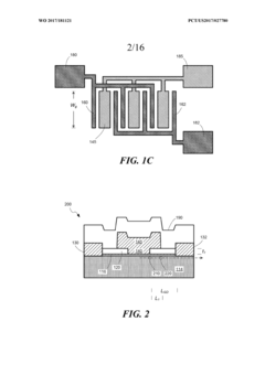
Gallium nitride superjunction devices
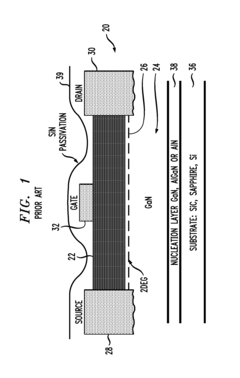
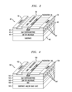
PatentInactiveUS20130240951A1
Innovation
- Incorporating a doped gallium nitride superjunction layer with a plurality of p/n junctions between the substrate and a barrier layer, which suppresses breakdown by modifying the electric field distribution, allowing for higher breakdown voltages and enabling the use of low-cost Si substrates.
Thermal Management Strategies for High-Voltage GaN
Thermal management represents a critical challenge in high-voltage GaN HEMT devices due to their high power density operation. As these devices operate at elevated voltages (>600V), they generate significant heat that must be efficiently dissipated to maintain reliability and performance. The thermal conductivity of GaN (130-230 W/m·K) is superior to silicon but inferior to SiC, creating unique thermal management requirements.
Several thermal management strategies have emerged as effective solutions for high-voltage GaN applications. Advanced packaging techniques utilizing direct bonded copper (DBC) substrates provide superior thermal pathways compared to traditional packaging. These substrates offer thermal resistance values below 0.5°C/W, enabling efficient heat transfer from the device to the heat sink.
Active cooling solutions incorporating microfluidic channels directly integrated into GaN device substrates have demonstrated remarkable cooling capabilities, reducing junction temperatures by up to 40°C compared to conventional cooling methods. This approach is particularly valuable for high-voltage applications where power densities can exceed 5 W/mm².
Novel substrate materials represent another frontier in thermal management. Diamond substrates, with thermal conductivity exceeding 2000 W/m·K, have shown promise in laboratory settings, potentially reducing thermal resistance by 75% compared to standard substrates. However, cost and manufacturing challenges currently limit widespread adoption.
Thermal simulation and modeling tools have become essential for optimizing device designs before fabrication. Three-dimensional finite element analysis enables precise prediction of hotspot formation and thermal gradients across the device structure. These simulations have proven accurate within 5% of experimental measurements, significantly reducing design iterations.
Innovative die-attach materials, particularly silver-sintered connections, provide superior thermal conductivity (>200 W/m·K) compared to conventional solders (50-70 W/m·K). These materials maintain excellent thermal performance even after thousands of thermal cycles, critical for high-voltage applications experiencing significant temperature fluctuations.
System-level thermal management approaches incorporating multiple cooling technologies have demonstrated the most promising results. Combinations of advanced substrates, optimized package designs, and efficient heat sinks have enabled GaN devices to operate reliably at junction temperatures below 150°C even when handling kilowatt-level power in high-voltage applications.
Reliability Assessment of GaN HEMTs in High-Voltage Systems
The reliability of GaN HEMTs in high-voltage applications represents a critical concern for power electronics system designers. These devices must maintain stable performance under extreme electrical, thermal, and environmental stresses over extended operational lifetimes. Current reliability assessment methodologies focus on accelerated life testing, where devices are subjected to conditions exceeding normal operational parameters to induce failure mechanisms that might otherwise take years to manifest.
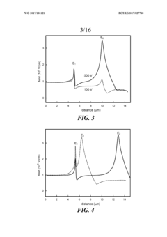
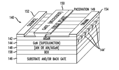
Time-dependent dielectric breakdown (TDDB) emerges as a primary reliability concern in high-voltage GaN HEMTs. This phenomenon occurs when the gate or buffer dielectric gradually degrades under sustained electric field stress, eventually leading to catastrophic failure. Research indicates that TDDB follows a Weibull distribution pattern, with lifetime strongly dependent on electric field strength according to the E-model or 1/E-model.
Dynamic Ron effects present another significant reliability challenge, particularly in power switching applications. This phenomenon manifests as an increase in on-resistance during switching operations, reducing efficiency and potentially causing thermal management issues. Studies have shown that dynamic Ron is influenced by trapping mechanisms at the AlGaN/GaN interface and in the buffer layers, with recovery times ranging from microseconds to hours depending on device architecture and operating conditions.
Hot electron degradation constitutes a third major reliability concern, occurring when electrons gain sufficient energy from the electric field to damage the semiconductor lattice or become trapped at interfaces. This degradation mechanism accelerates at higher voltages and can permanently alter threshold voltage and transconductance characteristics. Advanced device designs incorporating field plates and optimized channel geometries have demonstrated improved resistance to hot electron effects.
Standardized reliability assessment protocols have been developed by industry bodies such as JEDEC, with specific test methods for GaN power devices outlined in JEP180 and related documents. These protocols typically include high-temperature reverse bias (HTRB) testing, high-temperature gate bias (HTGB) testing, and temperature-humidity-bias (THB) testing to evaluate different failure modes.
Statistical analysis plays a crucial role in reliability assessment, with techniques such as Weibull plotting and mean time to failure (MTTF) calculations providing quantitative metrics for device lifetime prediction. Monte Carlo simulations incorporating multiple stress factors are increasingly employed to model complex failure mechanisms and their interactions in high-voltage applications.
Recent advancements in reliability testing include the development of on-wafer reliability assessment techniques that enable earlier identification of potential failure modes, reducing development cycles and improving yield rates for high-voltage GaN HEMT manufacturing processes.
Unlock deeper insights with Patsnap Eureka Quick Research — get a full tech report to explore trends and direct your research. Try now!
Generate Your Research Report Instantly with AI Agent
Supercharge your innovation with Patsnap Eureka AI Agent Platform!