Comparison Of Lateral Versus Vertical GaN HEMT Structures
SEP 5, 20259 MIN READ
Generate Your Research Report Instantly with AI Agent
Patsnap Eureka helps you evaluate technical feasibility & market potential.
GaN HEMT Evolution and Development Objectives
Gallium Nitride (GaN) High Electron Mobility Transistors (HEMTs) have emerged as revolutionary power semiconductor devices, offering superior performance characteristics compared to traditional silicon-based technologies. The evolution of GaN HEMTs began in the early 1990s with fundamental research on wide bandgap semiconductors, progressing through significant technological milestones that have shaped today's commercial landscape.
The initial development phase focused on lateral GaN HEMT structures, leveraging the two-dimensional electron gas (2DEG) formed at the AlGaN/GaN heterojunction interface. This configuration demonstrated exceptional electron mobility and high carrier concentration without intentional doping, establishing the foundation for high-frequency and high-power applications. Early research concentrated primarily on RF applications for defense and telecommunications sectors.
By the early 2000s, researchers began addressing critical challenges including current collapse phenomena, gate leakage, and thermal management issues. The introduction of field plates, advanced passivation techniques, and novel buffer layer designs marked significant advancements in device reliability and performance. During this period, the first commercial GaN RF devices entered the market, primarily targeting wireless infrastructure applications.
The mid-2010s witnessed a paradigm shift with increased attention toward vertical GaN HEMT architectures. This evolution was driven by the fundamental limitations of lateral structures in high-voltage applications, particularly the trade-off between breakdown voltage and on-resistance. Vertical structures offered a more favorable scaling of these parameters, potentially enabling GaN technology to address higher voltage applications beyond 1200V.
Current technological trajectories aim to optimize both lateral and vertical architectures for specific application domains. Lateral GaN HEMTs continue to dominate RF and medium-voltage (below 900V) power conversion applications, while vertical structures show promising potential for high-voltage power electronics exceeding 1200V. The development objectives now focus on achieving theoretical performance limits while addressing manufacturing scalability and cost reduction.
Looking forward, research objectives include enhancing thermal performance through advanced packaging and substrate technologies, improving dynamic performance through novel gate drive and circuit topologies, and developing application-specific integrated solutions that maximize GaN's inherent advantages. Additionally, there is growing emphasis on developing normally-off (enhancement-mode) devices to simplify circuit design and improve system safety.
The ultimate technical goal remains achieving the theoretical performance limits of GaN material while establishing manufacturing processes that enable cost-competitive production at scale. This includes reducing defect densities, optimizing epitaxial growth processes, and developing standardized reliability testing methodologies that accurately predict device lifetime under various operating conditions.
Market Analysis for GaN Power Electronics
The global GaN power electronics market is experiencing robust growth, projected to reach $1.75 billion by 2026 with a CAGR of approximately 22.9% from 2021. This significant expansion is driven by the superior performance characteristics of GaN-based devices compared to traditional silicon solutions, particularly in high-frequency and high-power applications.
The automotive sector represents the largest market segment for GaN power electronics, accounting for nearly 32% of the total market share. The rapid adoption of electric vehicles (EVs) and the need for efficient power conversion systems have accelerated demand for GaN HEMTs in onboard chargers, DC-DC converters, and traction inverters. The automotive industry's push toward higher voltage systems (800V and beyond) further enhances GaN's value proposition.
Consumer electronics constitutes the second-largest market segment at 27%, with applications in fast chargers, wireless power systems, and high-efficiency power supplies. The telecommunications sector follows at 18%, primarily utilizing GaN technology in base station power amplifiers and infrastructure equipment. Industrial applications represent 15% of the market, while renewable energy systems account for 8%.
Regionally, Asia-Pacific dominates the GaN power electronics market with 45% share, driven by extensive manufacturing capabilities in China, Japan, and South Korea. North America follows at 30%, with significant research activities and early adoption in defense and aerospace applications. Europe represents 20% of the market, with strong growth in automotive and industrial sectors.
When comparing lateral versus vertical GaN HEMT structures in market context, lateral devices currently dominate commercial applications with approximately 85% market share due to their manufacturing maturity and established supply chains. However, vertical GaN HEMTs are gaining attention for higher voltage applications (>1200V) and are expected to capture 25% of the high-power segment by 2025.
The market dynamics between these two structures are evolving rapidly. Lateral GaN HEMTs maintain advantages in medium-voltage (650V) applications and cost-effectiveness, while vertical structures offer superior performance in high-current density applications. Industry analysts predict that as manufacturing processes for vertical GaN HEMTs mature and costs decrease, their market share will expand significantly, particularly in electric vehicle powertrains and grid-connected power systems.
Technical Challenges in Lateral vs Vertical GaN HEMTs
Despite significant advancements in GaN HEMT technology, both lateral and vertical structures face distinct technical challenges that limit their performance and widespread adoption. Lateral GaN HEMTs, which currently dominate the commercial market, encounter fundamental limitations in power handling capability due to their device geometry. The lateral configuration inherently restricts current flow to a two-dimensional channel, creating current crowding effects near the gate edge that lead to localized heating and reliability concerns.
Surface-related issues present another major challenge for lateral structures. The exposed surface between gate and drain is particularly susceptible to electron trapping phenomena, resulting in current collapse and dynamic RON degradation. These surface states significantly impact device stability during high-voltage switching operations, necessitating complex passivation techniques that add manufacturing complexity.
Thermal management remains problematic in lateral devices due to the heat generation occurring close to the device surface. The thermal resistance pathway through the substrate creates bottlenecks for heat dissipation, especially in high-power applications where efficient cooling becomes critical for reliable operation.
For vertical GaN HEMTs, the primary technical hurdle lies in obtaining high-quality, thick GaN substrates with low defect densities. The heteroepitaxial growth of GaN on foreign substrates introduces threading dislocations that propagate through the active device regions, degrading carrier mobility and breakdown characteristics. Native GaN substrates remain prohibitively expensive for mass production, creating a significant barrier to commercialization.
Channel formation and control present unique challenges in vertical structures. Unlike lateral devices where the 2DEG forms naturally at the AlGaN/GaN interface, vertical devices require precise doping control to form conductive channels. Achieving uniform doping profiles throughout the thick drift regions while maintaining high breakdown voltage capabilities demands sophisticated epitaxial growth techniques.
Edge termination design is particularly challenging for vertical GaN HEMTs. The management of electric field crowding at device peripheries requires specialized termination structures that add process complexity. Without proper edge termination, premature breakdown occurs, preventing the device from reaching its theoretical performance limits.
Fabrication processes for vertical structures are less mature compared to lateral counterparts. Critical processes such as deep etching with minimal damage, formation of reliable ohmic contacts on p-GaN, and development of stable gate structures require significant refinement before vertical GaN HEMTs can achieve manufacturing readiness comparable to lateral devices.
Current Lateral and Vertical GaN HEMT Design Approaches
01 Lateral GaN HEMT Structure Design
Lateral GaN HEMTs feature a horizontal current flow parallel to the device surface. These structures typically include an AlGaN barrier layer on top of a GaN channel layer, creating a two-dimensional electron gas (2DEG) at the interface. Key design elements include gate configuration, field plates for field management, and source/drain contact optimization. Lateral structures are widely used in commercial applications due to their simpler fabrication process and excellent high-frequency performance.- Lateral GaN HEMT Structure Design: Lateral GaN HEMTs feature a horizontal current flow parallel to the device surface. These structures typically include an AlGaN barrier layer on top of a GaN channel layer, creating a two-dimensional electron gas (2DEG) at the interface. Key design elements include gate configuration, field plates for field management, and source/drain contact optimization. Lateral structures are widely used in RF and power applications due to their excellent high-frequency performance and relatively simpler fabrication process compared to vertical structures.
- Vertical GaN HEMT Architecture: Vertical GaN HEMTs feature a current flow perpendicular to the device surface, allowing for higher current density and voltage handling capability. These structures typically incorporate a thick GaN drift layer and utilize the entire substrate thickness for voltage blocking. Vertical architectures can achieve higher power density and better thermal performance than lateral structures, making them suitable for high-power applications. The design often includes specialized buffer layers and substrate considerations to manage the vertical current flow efficiently.
- Performance Comparison Between Lateral and Vertical GaN HEMTs: Vertical GaN HEMTs generally offer superior power handling capabilities and lower on-resistance compared to lateral structures, especially at higher voltages. However, lateral structures typically demonstrate better high-frequency performance and are more mature in terms of manufacturing processes. Thermal management differs significantly between the two architectures, with vertical structures showing advantages in heat dissipation. The breakdown voltage scaling also differs, with vertical structures showing more favorable scaling with device area, while lateral devices require more complex field management techniques to achieve comparable voltage ratings.
- Novel Materials and Fabrication Techniques for GaN HEMTs: Advanced materials and fabrication techniques are being developed to enhance both lateral and vertical GaN HEMT performance. These include novel buffer layer compositions, alternative substrates like silicon carbide or diamond, and specialized epitaxial growth methods. Techniques such as selective area growth, regrowth processes for contacts, and advanced etching methods are employed to optimize device characteristics. Surface passivation techniques and gate dielectric engineering are also critical for improving reliability and reducing current collapse phenomena in both structure types.
- Hybrid and Novel GaN HEMT Structures: Researchers are developing hybrid and novel GaN HEMT structures that combine aspects of both lateral and vertical designs to leverage their respective advantages. These include quasi-vertical structures, fin-based architectures, and multi-channel designs. Some approaches incorporate polarization engineering, novel heterojunctions, or three-dimensional structures to enhance performance. These hybrid approaches aim to achieve higher breakdown voltage, lower on-resistance, and better thermal performance while maintaining the fabrication advantages of conventional structures.
02 Vertical GaN HEMT Architecture
Vertical GaN HEMTs feature a current flow perpendicular to the substrate surface, allowing for higher current density and voltage handling capability compared to lateral structures. These devices typically incorporate a thick GaN drift layer and utilize the third dimension for improved power handling. The vertical architecture enables smaller device footprints while maintaining high breakdown voltages, making them particularly suitable for high-power applications where area efficiency is critical.Expand Specific Solutions03 Performance Comparison Between Lateral and Vertical GaN HEMTs
Vertical GaN HEMTs generally offer superior power handling capabilities and higher breakdown voltages compared to lateral structures, while lateral devices typically excel in high-frequency applications. Vertical structures demonstrate better thermal management due to more efficient heat dissipation paths and reduced current crowding. However, lateral structures currently benefit from more mature fabrication processes and lower manufacturing costs. The choice between structures depends on specific application requirements balancing power density, operating frequency, and thermal considerations.Expand Specific Solutions04 Advanced Buffer and Substrate Technologies
Buffer layer design and substrate selection significantly impact GaN HEMT performance in both lateral and vertical configurations. Silicon, silicon carbide, and native GaN substrates each offer different trade-offs in terms of cost, thermal conductivity, and lattice matching. Advanced buffer technologies include step-graded transition layers, carbon or iron doping for leakage suppression, and nucleation layers to manage stress. These technologies help mitigate issues like current collapse and buffer trapping that affect device reliability and performance.Expand Specific Solutions05 Novel Hybrid and Enhancement-Mode Structures
Innovative GaN HEMT designs combine elements of both lateral and vertical architectures to leverage their respective advantages. These hybrid structures aim to optimize power density while maintaining high-frequency capabilities. Additionally, enhancement-mode (normally-off) implementations using techniques such as p-GaN gates, fluorine plasma treatment, or recessed gate structures address the inherently depletion-mode (normally-on) nature of conventional GaN HEMTs. These advancements are critical for practical power switching applications requiring fail-safe operation.Expand Specific Solutions
Leading GaN Semiconductor Manufacturers and Research Institutions
The GaN HEMT market is currently in a growth phase, with lateral structures dominating commercial applications while vertical structures represent an emerging technology frontier. The global GaN power device market is projected to reach $1.5 billion by 2026, driven by demand for high-frequency, high-power applications. Lateral GaN HEMTs have reached commercial maturity with companies like Wolfspeed, Fujitsu, and TSMC leading production, while vertical GaN structures remain primarily in research stages. Key players like Infineon, HRL Laboratories, and Huawei are investing heavily in vertical GaN technology for its potential advantages in power density and breakdown voltage. University collaborations with industry partners, particularly from Chinese institutions and Taiwanese manufacturers, are accelerating development of both architectures for next-generation power electronics.
Taiwan Semiconductor Manufacturing Co., Ltd.
Technical Solution: TSMC has developed advanced GaN HEMT technologies focusing primarily on lateral structures for power and RF applications. Their GaN-on-Si technology platform features sophisticated buffer layer architectures that effectively manage the lattice mismatch and thermal expansion differences between GaN and silicon substrates. TSMC's lateral GaN HEMTs incorporate optimized AlGaN/GaN heterostructures with precise control of aluminum content and layer thickness to maximize carrier concentration in the 2DEG channel. Their manufacturing process includes advanced lithography techniques for gate formation with lengths down to 0.15μm for RF applications, and specialized field plate structures for power devices to enhance breakdown voltage. TSMC has also explored vertical GaN structures, though with less commercial emphasis, focusing on innovative drift region designs and specialized contact schemes to minimize on-resistance.
Strengths: World-class manufacturing infrastructure with exceptional process control; ability to integrate GaN with CMOS technologies; economies of scale reducing production costs. Weaknesses: Less experience with vertical GaN structures compared to lateral; primarily focused on GaN-on-Si which has thermal limitations compared to GaN-on-SiC for highest performance applications.
Wolfspeed, Inc.
Technical Solution: Wolfspeed has pioneered both lateral and vertical GaN HEMT structures, with particular expertise in lateral GaN-on-SiC HEMTs for RF applications. Their lateral GaN HEMT technology features advanced epitaxial layer structures with optimized AlGaN/GaN interfaces and field plates for enhanced breakdown voltage. For vertical structures, Wolfspeed has developed innovative drift region designs with controlled doping profiles to maximize current handling while maintaining high breakdown voltage. Their vertical GaN technology incorporates specialized trench gate structures and advanced termination techniques to manage electric fields at device edges. Wolfspeed's manufacturing processes include proprietary substrate preparation techniques and advanced MOCVD growth methods that minimize defect densities in both lateral and vertical structures.
Strengths: Industry-leading SiC substrate technology providing superior thermal management for lateral devices; extensive manufacturing infrastructure; advanced epitaxial growth expertise. Weaknesses: Higher cost structure compared to silicon-based alternatives; vertical GaN technology still faces commercialization challenges related to substrate availability and defect management.
Critical Patents and Breakthroughs in GaN HEMT Technology
Gallium nitride high electron mobility transistor structure
PatentActiveJP2008546175A
Innovation
- Implement a two-step AlN nucleation layer growth process, where the first layer is grown with an Al to reactive nitrogen ratio of less than 1 to prevent silicon migration, followed by a second layer with a ratio greater than 1 to improve material quality, using molecular beam epitaxy (MBE) to minimize silicon contamination.
High electron mobility transistor (HEMT) device
PatentActiveUS10734512B2
Innovation
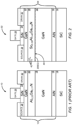
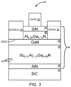
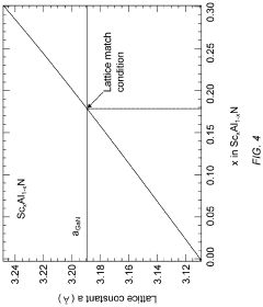
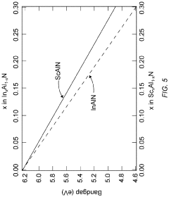
- Incorporating an aluminum (Al) based layer with a Group IIIB transition metal alloying element, such as scandium (Sc), in the epitaxial structure of HEMT devices to relieve lattice stress and maintain high sheet charge density, achieving a sheet charge density of 3.18×10^13/cm^2 with improved electron Hall mobility and reliability.
Thermal Management Solutions for GaN HEMT Devices
Thermal management represents a critical challenge in the development and operation of GaN HEMT devices, particularly when comparing lateral versus vertical structures. The inherent high power density capabilities of GaN HEMTs generate significant heat that must be efficiently dissipated to maintain device performance and reliability.
Lateral GaN HEMTs face particular thermal challenges due to their planar geometry, where heat is primarily concentrated in a narrow channel region. This creates localized hotspots that can reach temperatures exceeding 200°C during operation. Traditional cooling solutions for lateral structures include substrate thinning, flip-chip bonding, and the integration of heat spreaders, which have shown varying degrees of effectiveness.
Vertical GaN HEMT structures offer inherent thermal advantages through their three-dimensional architecture. The vertical current flow path allows for more uniform heat distribution throughout the device volume rather than concentrating it at the surface. Studies have demonstrated that vertical GaN HEMTs can achieve up to 40% lower thermal resistance compared to their lateral counterparts with equivalent power ratings.
Advanced thermal interface materials (TIMs) have emerged as crucial components for both structures. Diamond-based composites with thermal conductivities exceeding 1500 W/mK have shown promising results when integrated with GaN devices. For lateral structures, these materials are typically applied between the device and heat sink, while vertical structures benefit from their integration within the substrate itself.
Microfluidic cooling represents another frontier in thermal management, particularly beneficial for lateral GaN HEMTs. Direct liquid cooling channels fabricated beneath the active device region have demonstrated the ability to dissipate heat fluxes exceeding 1000 W/cm², significantly outperforming conventional air cooling methods. However, implementation challenges remain regarding integration complexity and long-term reliability.
Thermal simulation tools have become essential for optimizing device designs before fabrication. Three-dimensional finite element modeling allows engineers to predict temperature distributions with high accuracy, revealing that vertical structures typically exhibit more uniform thermal profiles compared to lateral devices under identical operating conditions.
Recent innovations include the development of heterogeneous integration approaches where GaN devices are bonded to high thermal conductivity substrates like silicon carbide or diamond. This technique has shown particular promise for lateral structures, reducing junction temperatures by up to 30% compared to conventional silicon substrates.
Manufacturing Process Comparison and Scalability Analysis
The manufacturing processes for lateral and vertical GaN HEMT structures differ significantly, with important implications for scalability and commercial viability. Lateral GaN HEMTs utilize a more established fabrication process that closely resembles conventional silicon CMOS manufacturing techniques. This similarity allows manufacturers to leverage existing semiconductor fabrication infrastructure with minimal modifications, resulting in lower initial capital investment requirements.
Lateral structures typically employ epitaxial growth on foreign substrates such as silicon, silicon carbide, or sapphire. The use of silicon substrates in particular offers substantial cost advantages, with 6-inch and 8-inch wafers being standard in production environments. This approach benefits from decades of manufacturing optimization in the silicon industry, enabling high yields and relatively straightforward process integration.
In contrast, vertical GaN HEMT structures require more specialized manufacturing processes. The fabrication typically demands high-quality bulk GaN substrates, which remain significantly more expensive and limited in availability compared to silicon substrates. Current commercial bulk GaN wafers are predominantly limited to 2-inch or 4-inch diameters, creating a substantial scalability disadvantage compared to lateral structures.
Vertical structures necessitate precise control of epitaxial growth throughout the entire device structure, requiring more sophisticated equipment and tighter process controls. The etching processes for vertical devices are particularly challenging, as they must create deep trenches with precise sidewall profiles while maintaining material quality. These requirements often translate to lower yields and higher manufacturing costs in current production environments.
From a scalability perspective, lateral GaN HEMTs currently hold a significant advantage. The established manufacturing ecosystem supports higher volume production with better economies of scale. Major semiconductor foundries have already implemented lateral GaN HEMT processes, allowing for relatively straightforward technology transfer and capacity expansion.
Vertical GaN technology, while promising for high-power applications, faces substantial scalability challenges. The limited availability of large-diameter bulk GaN substrates represents a critical bottleneck. However, ongoing research into alternative approaches, such as quasi-vertical structures on foreign substrates and improved GaN crystal growth techniques, may eventually address these limitations.
The manufacturing maturity gap between these technologies is reflected in their market presence. Lateral GaN HEMTs have achieved commercial success in various applications, while vertical structures remain predominantly in the research and development phase, with limited commercial deployment primarily in specialized high-power applications where their performance advantages justify the higher manufacturing costs.
Unlock deeper insights with Patsnap Eureka Quick Research — get a full tech report to explore trends and direct your research. Try now!
Generate Your Research Report Instantly with AI Agent
Supercharge your innovation with Patsnap Eureka AI Agent Platform!