Gate Drive Design Considerations For GaN HEMTs
SEP 5, 20259 MIN READ
Generate Your Research Report Instantly with AI Agent
PatSnap Eureka helps you evaluate technical feasibility & market potential.
GaN HEMT Technology Evolution and Design Goals
Gallium Nitride High Electron Mobility Transistors (GaN HEMTs) have evolved significantly since their inception in the early 1990s. Initially developed for military and aerospace applications due to their superior performance at high frequencies and temperatures, GaN HEMTs have undergone substantial refinement to address commercial power electronics markets. The technology evolution has been marked by progressive improvements in material quality, device structure optimization, and manufacturing processes.
The first generation of GaN HEMTs faced challenges with high defect densities and limited reliability. By the early 2000s, researchers had made significant strides in epitaxial growth techniques, reducing defect densities by several orders of magnitude. This period also saw the introduction of field plates to manage peak electric fields, substantially improving breakdown voltage characteristics and reliability.
Between 2005 and 2015, the focus shifted toward commercialization, with companies like EPC, GaN Systems, and Transphorm introducing GaN-on-Si technology to reduce manufacturing costs. This era witnessed critical advancements in surface passivation techniques and gate engineering to mitigate current collapse phenomena and dynamic RDS(on) issues that had previously limited widespread adoption.
Recent developments have centered on enhancing gate drive compatibility and robustness. The evolution from depletion-mode (normally-on) to enhancement-mode (normally-off) devices represents a pivotal advancement, making GaN HEMTs more compatible with conventional silicon-based gate drive circuits and improving system safety. Various gate technologies including recessed gate structures, p-GaN gates, and hybrid cascode configurations have emerged to address the normally-off requirement.
The primary design goals for modern GaN HEMT gate drive systems include achieving reliable switching at higher frequencies (>1 MHz), minimizing switching losses, and ensuring robust operation under various temperature and voltage conditions. Engineers aim to develop gate drivers capable of providing precise control over slew rates to balance EMI concerns with switching efficiency.
Another critical design objective is to enhance immunity to parasitic turn-on effects, which become increasingly problematic at higher switching speeds. This requires careful consideration of common-source inductance and Miller capacitance effects in both device and gate drive design.
Looking forward, the technology roadmap focuses on further integration of gate drive functionality with GaN power devices, potentially leading to monolithic or co-packaged solutions that minimize parasitic elements. Additionally, there is growing emphasis on developing intelligent gate drive systems capable of real-time adaptation to operating conditions, fault detection, and protection mechanisms specifically tailored to GaN's unique characteristics and failure modes.
Market Demand Analysis for GaN Power Electronics
The global market for Gallium Nitride (GaN) power electronics has witnessed remarkable growth in recent years, driven primarily by the increasing demand for high-efficiency power conversion systems across multiple industries. Current market valuations place the GaN power device market at approximately 1.1 billion USD in 2023, with projections indicating a compound annual growth rate (CAGR) of 25% through 2028, potentially reaching 3.4 billion USD by the end of the forecast period.
The automotive sector represents one of the most significant market opportunities for GaN power electronics, particularly in electric vehicle (EV) applications. The need for more efficient onboard chargers, DC-DC converters, and traction inverters has created substantial demand for GaN HEMTs with optimized gate drive designs. Industry reports suggest that automotive applications currently account for roughly 32% of the total GaN power device market, with this share expected to increase to 40% by 2026.
Consumer electronics constitutes another major market segment, where the push for smaller, more efficient power adapters has accelerated GaN adoption. The fast-charging segment for mobile devices has seen particularly strong growth, with GaN-based chargers capturing approximately 18% market share in 2023, up from just 5% in 2020. This rapid penetration demonstrates the market's recognition of GaN's superior performance characteristics when properly implemented with advanced gate drive solutions.
Industrial power supplies and renewable energy systems represent emerging high-growth segments for GaN technology. In solar inverters, the improved switching performance of GaN HEMTs with properly designed gate drives has enabled efficiency improvements of 2-3 percentage points compared to silicon-based solutions, translating to significant energy savings over system lifetimes. Market analysis indicates that the renewable energy sector's demand for GaN power devices is growing at 30% annually, outpacing the overall market average.
Telecommunications infrastructure, particularly for 5G deployment, has emerged as another significant market driver. The power density advantages of GaN-based power amplifiers and power supplies address the critical space and thermal management challenges in 5G base stations. Industry surveys indicate that approximately 45% of new 5G infrastructure deployments are incorporating GaN technology in some capacity, with gate drive optimization being a key focus area for reliability improvement.
Regional analysis reveals that Asia-Pacific currently dominates the GaN power electronics market with approximately 48% share, followed by North America (27%) and Europe (20%). China, Japan, and South Korea are particularly active in developing domestic GaN supply chains, with government initiatives supporting research and commercialization efforts focused on advanced gate drive technologies to maximize GaN HEMT performance and reliability.
Current Gate Drive Challenges for GaN HEMTs
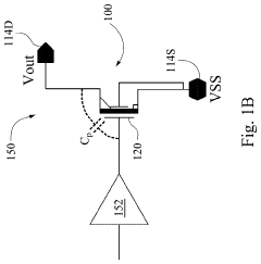
GaN HEMTs (Gallium Nitride High Electron Mobility Transistors) present unique gate drive challenges that differ significantly from traditional silicon-based power devices. The primary challenge stems from their extremely fast switching speeds, with transition times in the nanosecond range, which demands gate drivers capable of delivering precise timing control and clean signal edges to prevent parasitic turn-on events.
The narrow gate voltage operating window represents another critical challenge. Unlike silicon MOSFETs with typical gate voltage ranges of ±20V, GaN HEMTs operate within much tighter margins—typically +6V/-3V. This narrow window necessitates precise voltage regulation in gate drive circuits, as even minor overshoots can lead to device degradation or catastrophic failure.
Common mode transient immunity (CMTI) presents a significant hurdle in GaN gate drive design. The extremely high dv/dt rates (often exceeding 100V/ns) can induce spurious currents through parasitic capacitances in isolation barriers, potentially causing false triggering or isolation failures. Gate drivers must therefore incorporate advanced isolation technologies with CMTI ratings of 100V/ns or higher.
Layout considerations become paramount with GaN technology. The high-frequency operation amplifies the impact of parasitic inductances in gate drive loops, which can cause voltage ringing, EMI issues, and switching losses. Minimizing loop areas and implementing kelvin source connections are essential but challenging to execute effectively in practical designs.
Power loop inductance management represents another significant challenge. The interaction between gate and power loops can lead to cross-talk effects, where switching transients in the power loop induce unwanted voltages in the gate circuit. This phenomenon is particularly problematic in half-bridge configurations where high-side and low-side devices switch in complementary patterns.
Temperature sensitivity adds another layer of complexity. GaN threshold voltages typically exhibit negative temperature coefficients, meaning they decrease as temperature rises. Gate drive circuits must account for this behavior to prevent thermal runaway conditions, particularly in parallel device configurations.
Finally, the lack of standardization in GaN gate drive requirements across different manufacturers creates integration challenges. Unlike silicon devices with well-established gate drive parameters, GaN HEMTs from different vendors may have varying specifications for optimal drive voltages, current requirements, and protection features, complicating the design of universal gate drive solutions.
Mainstream Gate Drive Solutions for GaN HEMTs
01 Gate driver circuit design for GaN HEMTs
Gate driver circuits for GaN HEMTs require specialized design considerations due to the unique characteristics of these transistors. These circuits typically include components for controlling the switching speed, providing appropriate voltage levels, and ensuring stable operation. Advanced gate driver designs may incorporate features such as adjustable slew rates, protection against voltage spikes, and optimization for high-frequency operation to fully leverage the performance capabilities of GaN HEMTs.- Gate driver circuit design for GaN HEMTs: Gate driver circuits for GaN HEMTs require specialized design considerations due to the unique characteristics of these transistors. These circuits typically include components for controlling the switching speed, providing appropriate voltage levels, and ensuring reliable operation. The design must account for the lower gate threshold voltage and higher switching speeds of GaN HEMTs compared to silicon-based devices, while preventing gate oscillations and overvoltage conditions.
- Protection mechanisms for GaN HEMT gate drives: Protection mechanisms are essential in GaN HEMT gate drive designs to prevent damage from overcurrent, overvoltage, and thermal issues. These mechanisms may include fast-acting current limiting circuits, voltage clamping devices, and thermal shutdown features. Advanced protection schemes can detect fault conditions and respond within nanoseconds to protect the sensitive gate structure of GaN HEMTs, extending device lifetime and improving system reliability.
- Integrated gate driver solutions for GaN HEMTs: Integrated gate driver solutions combine the driver circuitry with protection features and sometimes power stage components in a single package or chip. These integrated solutions can optimize the performance of GaN HEMTs by minimizing parasitic inductances and capacitances, which is critical for high-frequency operation. They often include level-shifting capabilities, bootstrap circuits for high-side driving, and specialized timing control to maximize switching efficiency.
- Gate drive optimization for high-frequency switching: Optimizing gate drives for high-frequency switching in GaN HEMTs involves careful consideration of layout, component selection, and driving waveforms. Techniques include minimizing gate loop inductance, using separate turn-on and turn-off paths, and implementing active gate driving to control the switching trajectory. These optimizations help reduce switching losses, minimize electromagnetic interference, and enable operation at frequencies well beyond what is possible with silicon devices.
- Novel gate drive architectures for GaN power applications: Novel gate drive architectures for GaN power applications include resonant gate drivers, multi-level driving schemes, and adaptive driving techniques. These innovative approaches can significantly reduce gate driving losses, improve switching performance, and enhance overall system efficiency. Some designs incorporate digital control elements that can dynamically adjust gate drive parameters based on operating conditions, optimizing performance across varying loads and temperatures.
02 Protection mechanisms in GaN HEMT gate drives
Protection mechanisms are essential in GaN HEMT gate drive designs to prevent device failure due to overvoltage, overcurrent, or thermal issues. These mechanisms may include fast-acting current limiting circuits, temperature monitoring systems, and voltage clamping techniques. Implementing robust protection strategies helps to enhance the reliability and longevity of GaN HEMT-based power systems, particularly in high-power applications where device stress can be significant.Expand Specific Solutions03 Integration techniques for GaN HEMT gate drivers
Integration techniques for GaN HEMT gate drivers focus on combining the driver circuitry with other system components to optimize performance and reduce size. These approaches may involve monolithic integration of the driver with the GaN HEMT, embedding passive components within the package, or utilizing advanced packaging technologies. Integrated solutions can minimize parasitic elements, improve thermal management, and enhance overall system efficiency while reducing the physical footprint of the power conversion system.Expand Specific Solutions04 High-frequency optimization for GaN HEMT gate drives
High-frequency optimization techniques for GaN HEMT gate drives are designed to take advantage of the fast switching capabilities of these devices. These techniques include minimizing loop inductances, optimizing PCB layouts, implementing resonant gate driving methods, and using specialized components designed for high-frequency operation. By addressing the challenges associated with high-frequency switching, these optimizations enable GaN HEMTs to operate at their maximum potential, resulting in more efficient and compact power conversion systems.Expand Specific Solutions05 Multi-level and adaptive gate drive techniques for GaN HEMTs
Multi-level and adaptive gate drive techniques for GaN HEMTs involve dynamically adjusting the gate drive parameters based on operating conditions. These advanced approaches may include variable gate voltage levels, adaptive dead-time control, and intelligent switching strategies that respond to changes in load or temperature. By tailoring the gate drive characteristics to specific operating points, these techniques can optimize the trade-off between switching losses and conduction losses, leading to improved overall efficiency across a wide range of operating conditions.Expand Specific Solutions
Key Industry Players in GaN HEMT Ecosystem
The GaN HEMT gate drive design market is in a growth phase, characterized by increasing adoption across power electronics applications. The market is expanding rapidly due to GaN's superior performance over silicon, with projections showing significant growth in the coming years. Technologically, the field is maturing with companies at different development stages. Industry leaders like Wolfspeed, Texas Instruments, and ROHM have established commercial GaN solutions with advanced gate drive designs, while academic institutions (University of Electronic Science & Technology of China, Peking University) contribute fundamental research. Taiwan Semiconductor and UMC provide manufacturing infrastructure. Emerging players like Ganpower International and Nanjing Green Core are developing specialized solutions. The ecosystem shows a balance between established semiconductor companies and specialized GaN-focused entities, with collaboration between industry and academia driving innovation.
Wolfspeed, Inc.
Technical Solution: Wolfspeed has pioneered advanced gate drive designs specifically optimized for their SiC and GaN HEMT devices. Their approach focuses on minimizing parasitic inductances through innovative packaging techniques and optimized PCB layouts. Wolfspeed's gate drivers incorporate precise voltage control mechanisms that maintain optimal threshold levels while preventing gate oscillations. Their designs feature integrated temperature compensation circuits that adjust gate drive parameters based on device temperature, ensuring consistent performance across operating conditions. Wolfspeed has developed specialized protection circuits that respond within nanoseconds to overcurrent events, preventing device failure during fault conditions. Their gate drive solutions also incorporate advanced isolation technologies with high common-mode transient immunity (CMTI) ratings exceeding 100 kV/μs, essential for high-frequency switching applications where dv/dt rates are extreme.
Strengths: Industry-leading expertise in wide bandgap semiconductors with optimized gate drive solutions specifically designed for GaN HEMTs. Their designs achieve exceptional switching speeds while maintaining reliability. Weaknesses: Their solutions often require more complex implementation compared to silicon-based alternatives, potentially increasing system cost and design complexity.
Texas Instruments Incorporated
Technical Solution: Texas Instruments has developed comprehensive gate drive solutions for GaN HEMTs that address the unique challenges of these devices. Their LMG gate driver series incorporates precise timing control with propagation delays under 5ns and matching within 1ns between channels, critical for preventing shoot-through in half-bridge configurations. TI's integrated solutions feature adaptive dead-time control that dynamically adjusts based on load conditions, optimizing efficiency across operating points. Their gate drivers implement sophisticated protection mechanisms including overcurrent protection with response times under 100ns, overvoltage protection, and thermal shutdown capabilities. TI has also pioneered integrated power stage solutions that combine the GaN HEMT with optimized gate drive circuitry in a single package, minimizing parasitic inductances and enabling switching frequencies exceeding 2MHz while maintaining high efficiency.
Strengths: Highly integrated solutions that combine multiple protection features with precise timing control, simplifying system design while enhancing reliability. Their extensive ecosystem of supporting components creates complete solutions. Weaknesses: Some of their more advanced integrated solutions may limit design flexibility compared to discrete implementations, potentially constraining optimization for specific applications.
Critical Patents and Innovations in GaN Gate Drive Design
Transistor with source field plates and non-overlapping gate runner layers
PatentActiveUS20210143258A1
Innovation
- The design includes a field plate extending from the source runner layer or source contact layer, positioned coplanar with the gate runner layer, allowing it to overlap vertically with the metal gate layer, reducing parasitic capacitance and resistance without additional routings, thus enhancing size efficiency.
Gallium nitride high electron mobility transistor
PatentPendingUS20230395694A1
Innovation
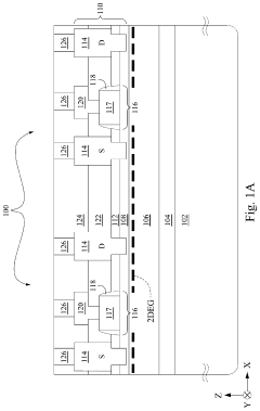
- The solution involves forming a second AlGaN layer with a different composition over the AlGaN-GaN heterojunction, using sidewall spacers and selective epitaxy to decouple on-resistance from the threshold voltage, achieved by increasing the aluminum concentration in the AlGaN layer and adjusting its thickness, thereby enhancing spontaneous and piezoelectric polarization effects.
Thermal Management Considerations for GaN Gate Drivers
Thermal management represents a critical aspect of GaN gate driver design due to the unique operational characteristics of GaN HEMTs. Unlike traditional silicon-based devices, GaN HEMTs operate at significantly higher switching frequencies and power densities, generating concentrated heat that must be effectively dissipated to maintain reliability and performance.
The thermal challenges in GaN gate driver circuits stem from multiple sources. First, the extremely fast switching speeds (often exceeding 100V/ns) create substantial power losses during switching transitions. Second, the compact packaging of modern GaN systems concentrates heat generation in smaller areas. Third, the gate driver IC itself generates heat while supplying the required current pulses for rapid charging and discharging of the GaN HEMT gate capacitance.
Temperature effects directly impact GaN HEMT performance parameters. As junction temperature rises, on-resistance increases, reducing efficiency and potentially creating thermal runaway conditions. Gate threshold voltage also exhibits temperature dependency, which can affect switching timing and potentially lead to shoot-through events if not properly managed. Research indicates that for every 10°C rise in temperature, GaN device lifetime may decrease by approximately 50%.
Effective thermal management strategies for GaN gate drivers include multi-layer PCB designs with dedicated thermal vias to enhance heat dissipation pathways. Copper pour areas connected to thermal pads provide essential heat spreading capabilities. Advanced packaging technologies such as flip-chip assemblies and embedded heat sinks are increasingly being adopted to address thermal challenges at the component level.
Thermal simulation has become an indispensable tool in GaN gate driver design. Computational fluid dynamics (CFD) and finite element analysis (FEA) enable designers to identify hotspots and optimize thermal pathways before physical prototyping. These simulations must account for the pulsed nature of gate driver operation and the resulting dynamic thermal profiles.
Active cooling solutions may be necessary for high-power applications. Forced-air cooling remains common, but liquid cooling systems are gaining traction for applications requiring extreme power density. Novel approaches utilizing phase-change materials and microfluidic cooling channels embedded within PCB structures represent emerging solutions for next-generation GaN systems.
Temperature monitoring and protection circuits form the final layer of thermal management. Integrated temperature sensors with fast response times can trigger protective actions before thermal damage occurs. Advanced gate drivers now incorporate temperature-dependent drive strength adjustment to maintain optimal switching performance across varying thermal conditions.
EMI/EMC Design Requirements for GaN-based Systems
GaN-based power systems present unique EMI/EMC challenges due to their high switching speeds and steep voltage transitions. The electromagnetic interference (EMI) generated by these systems can significantly impact nearby electronic components and systems if not properly managed. When designing gate drive circuits for GaN HEMTs, engineers must incorporate specific EMI/EMC considerations to ensure regulatory compliance and system reliability.
The primary EMI/EMC design requirements include careful PCB layout with minimized loop areas and strategic component placement. Power and ground planes should be properly designed with sufficient decoupling capacitors placed as close as possible to the GaN devices to minimize parasitic inductances. These measures help reduce both conducted and radiated emissions that result from the high dv/dt and di/dt characteristics of GaN switching.
Shielding techniques become essential in GaN-based systems, particularly for gate drive circuits which are susceptible to noise interference. Proper shielding can prevent external electromagnetic fields from affecting gate signals while also containing emissions generated by the switching action. The gate drive circuit should be physically isolated from power loops and sensitive analog circuits to prevent cross-coupling of electromagnetic energy.
Filtering requirements for GaN systems are more stringent compared to traditional silicon-based designs. Common mode chokes, ferrite beads, and specialized EMI filters must be incorporated at strategic locations to attenuate high-frequency noise. The gate drive path specifically requires careful filtering to prevent unwanted oscillations while maintaining the fast switching capability that makes GaN technology advantageous.
Grounding strategies play a crucial role in EMI/EMC compliance. A multi-point grounding approach is often necessary for GaN systems, with separate ground paths for power, gate drive, and signal circuits. Ground planes should be continuous and properly connected to minimize ground bounce effects that can lead to false triggering of the gate.
Signal integrity considerations must address the potential for crosstalk between high-speed switching nodes and sensitive gate drive signals. Differential signaling for gate drive inputs can improve noise immunity, while impedance matching and termination resistors help minimize signal reflections that could cause gate voltage instability.
Compliance testing for GaN-based systems typically requires meeting more stringent standards due to their higher operating frequencies. Designers must consider both conducted emissions (typically 150 kHz to 30 MHz) and radiated emissions (30 MHz to 1 GHz or higher) during the development phase, implementing pre-compliance testing early in the design cycle to identify potential issues.
Unlock deeper insights with PatSnap Eureka Quick Research — get a full tech report to explore trends and direct your research. Try now!
Generate Your Research Report Instantly with AI Agent
Supercharge your innovation with PatSnap Eureka AI Agent Platform!