Thermal Management Challenges For GaN HEMT Devices
SEP 5, 20259 MIN READ
Generate Your Research Report Instantly with AI Agent
Patsnap Eureka helps you evaluate technical feasibility & market potential.
GaN HEMT Thermal Management Background and Objectives
Gallium Nitride High Electron Mobility Transistors (GaN HEMTs) have emerged as revolutionary semiconductor devices in power electronics and RF applications over the past two decades. Their superior material properties, including wide bandgap (3.4 eV), high electron mobility, and high breakdown voltage, enable operation at higher frequencies, temperatures, and power densities compared to silicon-based technologies. However, the exceptional power density capabilities of GaN HEMTs introduce significant thermal management challenges that have become increasingly critical as the technology matures.
The evolution of GaN HEMT technology has been marked by continuous improvements in epitaxial growth techniques, device architectures, and substrate materials. Initially developed in the 1990s, GaN HEMTs have progressed from laboratory curiosities to commercial products driving applications in telecommunications, radar systems, and power conversion. This progression has been accompanied by escalating power densities, with modern devices capable of handling power densities exceeding 40 W/mm, creating unprecedented thermal management demands.
Thermal management has become the primary limiting factor in realizing the full potential of GaN technology. When operating at high power densities, localized heating occurs in the active region of these devices, creating "hotspots" that can reach temperatures exceeding 200°C. These elevated temperatures significantly impact device reliability, performance, and lifetime through mechanisms including electron trapping, accelerated degradation, and reduced carrier mobility.
The fundamental objective of thermal management research for GaN HEMTs is to develop innovative solutions that efficiently dissipate heat from the active device regions while maintaining electrical performance and reliability. This involves addressing challenges across multiple scales - from the atomic-level interfaces between materials to the system-level packaging and cooling strategies.
Current research aims to achieve several specific technical goals: reducing thermal boundary resistance between GaN and substrate materials; developing advanced substrate solutions with superior thermal conductivity; creating novel packaging approaches that minimize thermal resistance; implementing efficient heat spreading techniques; and designing intelligent thermal management systems that dynamically respond to operating conditions.
The trajectory of GaN HEMT development is increasingly influenced by thermal considerations, with industry roadmaps highlighting the need for breakthrough thermal management solutions to enable next-generation applications in 5G/6G communications, electric vehicles, renewable energy systems, and aerospace. As power densities continue to increase and form factors shrink, innovative approaches to thermal management will be essential to unlocking the full potential of this transformative semiconductor technology.
Market Demand Analysis for High-Performance GaN Devices
The global market for GaN HEMT (High Electron Mobility Transistor) devices is experiencing robust growth driven by increasing demand for high-performance power electronics across multiple sectors. Current market valuations indicate the GaN power device market reached approximately 223 million USD in 2022, with projections suggesting a compound annual growth rate (CAGR) of 33.4% through 2028, potentially reaching 1.24 billion USD by the end of the forecast period.
This accelerated market expansion stems primarily from the superior performance characteristics of GaN HEMTs compared to traditional silicon-based technologies. The demand is particularly strong in power electronics applications where efficiency, power density, and thermal performance are critical parameters. Industries including telecommunications, automotive, consumer electronics, and defense are actively seeking GaN solutions to address evolving requirements for smaller form factors and higher power capabilities.
In the telecommunications sector, the ongoing global deployment of 5G infrastructure represents a significant market driver. Base stations and network equipment manufacturers require RF power amplifiers with higher efficiency and power density, creating substantial demand for GaN HEMT devices. Market analysis indicates that approximately 65% of new 5G base stations are incorporating GaN technology in their RF components.
The automotive industry presents another high-growth segment, particularly with the rapid expansion of electric vehicles (EVs). GaN-based power conversion systems offer significant advantages in onboard chargers, DC-DC converters, and inverters. The market penetration of GaN in automotive applications is expected to grow at 42% annually through 2027, outpacing the overall GaN market growth rate.
Consumer electronics manufacturers are increasingly adopting GaN technology for fast-charging solutions. The market for GaN-based chargers grew by 52% in 2022 alone, with major smartphone and laptop manufacturers releasing GaN-enabled charging accessories. This consumer-facing application has significantly raised awareness of GaN benefits among end-users.
However, thermal management challenges represent a critical market constraint. Industry surveys indicate that 78% of design engineers cite thermal issues as the primary limitation when implementing GaN solutions. This creates a distinct market opportunity for advanced thermal management solutions specifically designed for GaN HEMT applications.
Regional analysis shows Asia-Pacific leading GaN device adoption, accounting for 43% of global market share, followed by North America at 31% and Europe at 22%. China, Japan, and South Korea are establishing themselves as manufacturing hubs for GaN technology, while North American and European markets focus more on high-value applications in defense and industrial sectors.
Current Thermal Challenges and Limitations in GaN HEMTs
GaN HEMT devices face significant thermal management challenges that limit their performance and reliability. The primary issue stems from the high power density operation of these devices, which can generate heat fluxes exceeding 10 kW/cm² in the active region. This concentrated heat generation creates localized hotspots that dramatically impact device performance and longevity.
The self-heating effect in GaN HEMTs presents a fundamental limitation, as the device's channel temperature can rise significantly above the case temperature during operation. Temperature increases of 100-150°C above ambient are commonly observed, with hotspot temperatures potentially reaching over 200°C in high-power applications. This thermal gradient accelerates various degradation mechanisms and reduces the mean time to failure.
Current thermal bottlenecks include the thermal boundary resistance (TBR) between the GaN and substrate materials, which impedes efficient heat dissipation. For devices built on silicon carbide (SiC) substrates, this TBR can account for 30-40% of the total thermal resistance. Devices on silicon substrates face even greater challenges due to silicon's inferior thermal conductivity compared to SiC.
The gate-drain access region experiences particularly severe thermal stress due to high electric fields and current densities. This area often becomes the critical failure point in high-power operation, with temperature increases causing electron mobility degradation that further exacerbates the heating problem through a positive feedback mechanism.
Package-level thermal management presents additional challenges. Traditional packaging solutions often cannot adequately address the extreme thermal demands of GaN HEMTs. The thermal resistance of die-attach materials, substrate interfaces, and package-to-heatsink connections creates a cumulative thermal bottleneck that limits the device's maximum operating power.
Transient thermal effects pose another significant challenge. During pulsed operation, rapid temperature fluctuations can cause mechanical stress due to coefficient of thermal expansion (CTE) mismatches between different device materials. These thermal cycles accelerate fatigue mechanisms and can lead to delamination, crack formation, and ultimately device failure.
Measurement and modeling limitations further complicate thermal management efforts. Accurate temperature measurement at the nanoscale remains challenging, while thermal simulation models often struggle to capture the complex three-dimensional heat flow patterns in these devices. This creates uncertainty in thermal design margins and can lead to either over-conservative designs or unexpected thermal failures.
The trade-off between thermal performance and other device parameters represents another limitation. Design modifications to improve thermal dissipation often negatively impact electrical performance, cost, or manufacturability, forcing difficult engineering compromises that ultimately constrain the technology's capabilities.
Current Thermal Dissipation Approaches for GaN HEMTs
01 Heat dissipation structures for GaN HEMT devices
Various heat dissipation structures can be integrated into GaN HEMT devices to improve thermal management. These structures include heat sinks, thermal vias, and specialized substrates that facilitate efficient heat transfer away from the active device regions. By incorporating these structures, the operating temperature of GaN HEMTs can be reduced, leading to improved device performance and reliability. Advanced materials with high thermal conductivity are often used in these structures to maximize heat dissipation efficiency.- Heat dissipation structures for GaN HEMT devices: Various heat dissipation structures can be implemented in GaN HEMT devices to improve thermal management. These structures include heat sinks, thermal vias, and specialized substrate materials that efficiently conduct heat away from the active device regions. By incorporating these structures, the thermal resistance of the device can be reduced, allowing for better heat dissipation and improved device performance under high-power operation conditions.
- Diamond-based thermal management solutions: Diamond materials are increasingly being used in GaN HEMT thermal management due to their exceptional thermal conductivity. Integration of diamond layers, either as substrates or as heat spreading layers, can significantly enhance heat dissipation from the active device regions. Various approaches include CVD diamond growth, diamond composite substrates, and diamond heat spreaders attached to conventional device structures, all aimed at leveraging diamond's superior thermal properties to manage the high heat flux in GaN power devices.
- Advanced packaging techniques for thermal management: Specialized packaging techniques play a crucial role in managing heat in GaN HEMT devices. These include flip-chip bonding, advanced die-attach materials with high thermal conductivity, and innovative package designs that minimize thermal resistance from junction to case. Some approaches incorporate direct liquid cooling channels within the package, while others utilize advanced thermal interface materials to improve heat transfer to external cooling systems.
- Thermal simulation and modeling approaches: Computational methods for thermal simulation and modeling are essential for optimizing GaN HEMT thermal management. These approaches include finite element analysis, computational fluid dynamics, and multi-physics simulations that account for the coupled electro-thermal behavior of these devices. Advanced modeling techniques help predict hotspot formation, thermal gradients, and transient thermal response, enabling designers to optimize device layouts and cooling strategies before fabrication.
- Novel substrate and buffer layer designs: Innovative substrate and buffer layer designs are being developed to address thermal challenges in GaN HEMT devices. These include engineered substrates with high thermal conductivity materials, thermally optimized transition layers, and novel epitaxial structures that minimize thermal boundary resistance. Some approaches incorporate patterned substrates or buried heat spreading layers to provide more efficient thermal paths away from the active device region, while others focus on reducing defect densities that can create localized heating.
02 Diamond-based thermal management solutions
Diamond materials are increasingly being utilized in GaN HEMT thermal management due to their exceptional thermal conductivity. Integration of diamond layers, either as substrates or as heat spreading layers, can significantly enhance heat dissipation from the device. Various techniques for diamond integration include diamond CVD growth, diamond composite substrates, and diamond heat spreaders. These diamond-based solutions help to address the thermal challenges associated with high-power GaN HEMT operation, enabling higher power densities and improved reliability.Expand Specific Solutions03 Advanced packaging techniques for thermal management
Innovative packaging approaches play a crucial role in managing heat in GaN HEMT devices. These techniques include flip-chip bonding, embedded heat pipes, advanced thermal interface materials, and three-dimensional integration methods. Such packaging solutions aim to minimize thermal resistance between the device and the heat sink, enabling more efficient heat extraction. By optimizing the thermal path from junction to ambient, these packaging techniques help maintain lower operating temperatures and extend device lifetime under high-power conditions.Expand Specific Solutions04 Active cooling systems for GaN HEMTs
Active cooling systems provide enhanced thermal management for high-power GaN HEMT applications. These systems include microfluidic cooling channels, thermoelectric coolers, and forced-air cooling mechanisms integrated with the device or package. By actively removing heat rather than relying solely on passive dissipation, these approaches can maintain lower junction temperatures even under extreme operating conditions. Active cooling is particularly valuable in applications where GaN HEMTs are operated at their power limits or in challenging environmental conditions.Expand Specific Solutions05 Thermal simulation and modeling techniques
Thermal simulation and modeling techniques are essential for optimizing the thermal management of GaN HEMT devices. These approaches include finite element analysis, computational fluid dynamics, and multi-physics simulations that predict temperature distributions and identify thermal bottlenecks. Advanced modeling techniques help engineers design more effective thermal management solutions by providing insights into heat flow patterns and temperature gradients within the device structure. These simulation tools enable iterative optimization of device layouts and cooling strategies before physical implementation.Expand Specific Solutions
Key Industry Players in GaN HEMT Thermal Solutions
The thermal management challenges for GaN HEMT devices are currently at a critical development stage, with the market experiencing rapid growth due to increasing demand in power electronics, telecommunications, and defense applications. The global GaN power device market is projected to reach several billion dollars by 2026, driven by advantages in high-frequency operation and power density. Leading companies like GaN Systems, RFHIC Corp, and Huawei Technologies are advancing cooling solutions through innovative substrate materials and packaging techniques, while research institutions such as Xidian University and IMEC are focusing on fundamental thermal characterization methodologies. Mitsubishi Electric, Qualcomm, and Lockheed Martin are integrating GaN technology into commercial and defense applications, addressing thermal challenges through system-level approaches to maintain reliability and performance.
GaN Systems, Inc.
Technical Solution: GaN Systems has developed an innovative thermal management approach for GaN HEMT devices that combines advanced packaging techniques with optimized thermal interface materials. Their solution incorporates a proprietary Direct Drive GaN architecture that reduces thermal resistance by eliminating wire bonds and utilizing copper-filled vias for direct heat extraction from the device junction. The company's thermal management system employs a multi-layer approach with sintered silver die-attach materials that provide superior thermal conductivity (>200 W/mK) compared to traditional solder materials. GaN Systems has also pioneered the use of embedded cooling channels within their package designs, allowing for more efficient heat dissipation in high-power density applications. Their thermal simulation models accurately predict junction temperatures within 5% of measured values, enabling precise thermal design optimization for customers implementing GaN power solutions.
Strengths: Industry-leading thermal resistance values (<0.5°C/W for certain package types); comprehensive thermal modeling tools for customers; compatible with standard PCB manufacturing processes. Weaknesses: Higher initial cost compared to silicon solutions; requires specialized design knowledge for optimal thermal performance; limited to certain package configurations.
Northrop Grumman Systems Corp.
Technical Solution: Northrop Grumman has developed specialized thermal management solutions for GaN HEMT devices used in defense and aerospace applications where reliability under extreme conditions is critical. Their approach incorporates advanced composite materials with tailored thermal expansion coefficients to minimize stress at material interfaces during thermal cycling. Northrop's thermal management system utilizes vapor chamber cooling technology with proprietary working fluids optimized for the high heat flux densities of GaN devices (>1000 W/cm²). Their solution includes multi-layer thermal stacks with diamond-copper composite materials that provide thermal conductivity exceeding 800 W/mK while maintaining mechanical robustness for aerospace applications. Northrop Grumman has also developed specialized thermal interface materials that maintain performance integrity even under high-G forces and vibration environments typical in military systems. Their thermal design methodology incorporates comprehensive reliability testing including accelerated thermal cycling and power cycling to ensure long-term performance in mission-critical applications.
Strengths: Exceptional reliability under extreme environmental conditions; proven performance in military/aerospace applications; comprehensive qualification testing protocols. Weaknesses: Very high cost structure; limited commercial availability outside defense applications; solutions often customized for specific military programs rather than general commercial use.
Critical Heat Transfer Technologies for GaN Devices
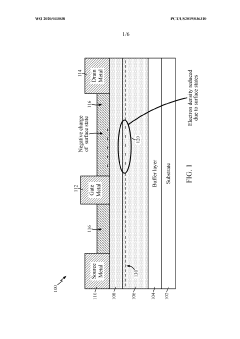
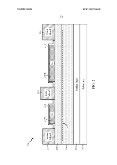
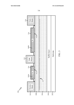
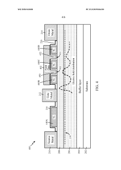
Gallium nitride high electron mobility transistor with ledges and field plates
PatentWO2020033038A1
Innovation
- Incorporating n-doped protuberances, or ledges, between the gate and source/drain electrodes, and optionally using field plates, to reduce surface states and increase channel electron density, thereby enhancing breakdown voltage and switching efficiency.
Gallium nitride high electron mobility transistor having high breakdown voltage and formation method therefor
PatentInactiveEP3591708A1
Innovation
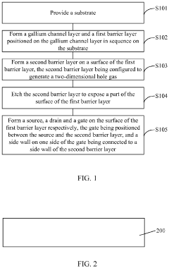
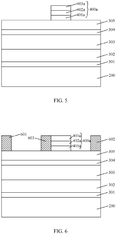
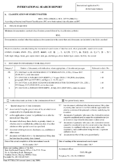
- A gallium nitride high electron mobility transistor with a second barrier layer configured to generate two-dimensional hole gas, positioned between the gate and drain, smoothes electric field distribution and improves breakdown voltage, comprising a substrate, gallium nitride channel layer, first and second barrier layers, and source and drain structures.
Reliability and Lifetime Assessment of GaN HEMTs Under Thermal Stress
The reliability and lifetime assessment of GaN HEMTs under thermal stress represents a critical aspect of device qualification for high-power applications. Thermal stress significantly impacts device degradation mechanisms, with junction temperature being the primary factor affecting long-term reliability. Studies indicate that for every 10°C increase in operating temperature above recommended levels, the mean time to failure (MTTF) can decrease by approximately 50%, highlighting the importance of accurate thermal characterization.
Accelerated life testing (ALT) methodologies have been developed specifically for GaN HEMTs, employing elevated temperatures to induce failure mechanisms that would otherwise take years to manifest. These tests typically involve operating devices at temperatures ranging from 150°C to 300°C while monitoring key electrical parameters such as threshold voltage shift, on-resistance increase, and gate leakage current. The Arrhenius model remains the predominant approach for extrapolating high-temperature test results to normal operating conditions, though recent research suggests modifications may be necessary to account for GaN-specific degradation physics.
Time-dependent dielectric breakdown (TDDB) and hot electron effects emerge as primary failure mechanisms under thermal stress. TDDB in the gate dielectric becomes particularly pronounced at elevated temperatures, with activation energies typically measured between 0.3-0.7 eV depending on device architecture and materials. Concurrently, hot electron effects accelerate at higher temperatures, causing threshold voltage instability and transconductance degradation.
Lifetime prediction models have evolved from simple Arrhenius-based calculations to more sophisticated multi-parameter models incorporating both electrical and thermal stress factors. Current industry standards suggest that properly designed GaN HEMTs should maintain reliability metrics for 10⁶ hours (approximately 114 years) at a junction temperature of 150°C, though this varies significantly based on device design and application requirements.
Non-destructive reliability assessment techniques have gained prominence, including low-frequency noise measurements and pulsed I-V characterization, which can detect early indicators of degradation before catastrophic failure occurs. These methods enable more accurate lifetime predictions without requiring device destruction, facilitating improved screening protocols during manufacturing.
Field reliability data increasingly demonstrates that laboratory assessments may underestimate certain failure modes, particularly those related to thermal cycling and temperature gradients across the device structure. This has prompted the development of mission profile-based reliability assessment frameworks that incorporate actual application conditions rather than steady-state thermal stress alone.
Integration Challenges with Existing Power Electronics Systems
The integration of GaN HEMT devices into existing power electronics systems presents significant challenges due to their unique thermal characteristics and operational requirements. Traditional silicon-based power electronics systems were designed with thermal management solutions tailored to silicon's thermal conductivity and operating temperature ranges. GaN HEMTs, with their higher power densities and operating temperatures, require substantial modifications to these established systems.
One primary integration challenge involves redesigning printed circuit boards (PCBs) to accommodate the enhanced thermal dissipation needs of GaN devices. Conventional PCB layouts and thermal vias designed for silicon devices often prove inadequate for GaN's concentrated heat generation. This necessitates the development of specialized PCB designs with optimized thermal pathways and potentially embedded cooling structures.
The interface materials between GaN devices and heat sinks represent another critical integration hurdle. Traditional thermal interface materials (TIMs) may not provide sufficient thermal conductivity for GaN applications. Advanced TIMs with higher thermal conductivity and reliability at elevated temperatures must be incorporated, often requiring changes to manufacturing processes and assembly techniques.
Cooling system compatibility presents further complications. Existing forced-air or liquid cooling systems may require significant modifications or complete redesign to handle the thermal loads generated by GaN HEMTs. The transition from silicon to GaN often necessitates more aggressive cooling solutions, potentially increasing system complexity, cost, and size—contradicting the miniaturization advantages that GaN technology offers.
Control systems and thermal protection mechanisms also require adaptation. GaN devices exhibit different thermal time constants and temperature-dependent performance characteristics compared to silicon devices. Existing thermal protection circuits and algorithms may respond inappropriately to GaN's thermal behavior, potentially causing false triggers or failing to protect devices adequately.
From a system architecture perspective, the integration of GaN HEMTs may necessitate reconsidering power stage layouts and component placements. The higher switching frequencies enabled by GaN create new electromagnetic interference (EMI) challenges that interact with thermal management solutions, requiring holistic design approaches that address both thermal and electromagnetic considerations simultaneously.
Cost considerations further complicate integration efforts. While GaN devices offer performance advantages, the additional expense of specialized thermal management solutions can erode their economic benefits. System designers must carefully balance performance improvements against increased thermal management costs to ensure commercial viability.
Unlock deeper insights with Patsnap Eureka Quick Research — get a full tech report to explore trends and direct your research. Try now!
Generate Your Research Report Instantly with AI Agent
Supercharge your innovation with Patsnap Eureka AI Agent Platform!