Photovoltaic Inverter Efficiency Improvements Using GaN HEMTs
SEP 5, 202510 MIN READ
Generate Your Research Report Instantly with AI Agent
Patsnap Eureka helps you evaluate technical feasibility & market potential.
GaN HEMT Technology Background and Efficiency Goals
Gallium Nitride High Electron Mobility Transistors (GaN HEMTs) represent a revolutionary advancement in semiconductor technology that has been developing since the early 1990s. These wide-bandgap semiconductor devices have emerged as superior alternatives to traditional silicon-based power transistors, particularly in high-frequency, high-power applications. The evolution of GaN technology has accelerated significantly over the past decade, transitioning from primarily research-focused development to commercial viability across multiple industries.
In the context of photovoltaic (PV) inverters, efficiency has been a persistent challenge. Traditional silicon-based inverters typically achieve efficiency ratings between 95-98%, with energy losses occurring primarily during the DC-AC conversion process. These losses manifest as heat, requiring substantial cooling systems that increase system complexity, size, and cost while reducing reliability. The photovoltaic industry has established ambitious efficiency targets exceeding 99% for next-generation inverters, driving the exploration of alternative semiconductor materials.
GaN HEMTs offer several inherent advantages that align perfectly with these efficiency goals. Their wide bandgap (3.4 eV compared to silicon's 1.1 eV) enables operation at higher voltages, temperatures, and switching frequencies. The high electron mobility characteristic allows for faster switching with minimal resistive losses during both on and off states. These properties directly address the primary sources of inefficiency in traditional inverter designs.
The technical trajectory of GaN HEMT development has focused on increasing power density while simultaneously reducing costs. Early iterations faced challenges related to substrate quality, thermal management, and reliability under high-stress conditions. Recent advancements have largely overcome these limitations, with current commercial GaN devices demonstrating remarkable performance improvements compared to their silicon counterparts.
For photovoltaic applications specifically, the efficiency targets include reducing switching losses by at least 50%, decreasing conduction losses by 30-40%, and enabling operation at junction temperatures up to 25°C higher than silicon equivalents. These improvements collectively aim to push inverter efficiency beyond 99%, while simultaneously reducing cooling requirements and overall system size by 25-30%.
The broader technological goal extends beyond mere efficiency gains to include enhanced reliability metrics. GaN-based inverters target a 50% increase in mean time between failures (MTBF) compared to silicon equivalents, with operational lifespans exceeding 25 years to match modern solar panel warranties. Additionally, there are aspirations to reduce electromagnetic interference (EMI) by leveraging the faster switching capabilities of GaN, potentially simplifying filtering requirements and further reducing system complexity.
Market Demand Analysis for High-Efficiency PV Inverters
The global photovoltaic (PV) inverter market is experiencing robust growth driven by increasing renewable energy adoption and the push for higher efficiency systems. Current market analysis indicates that high-efficiency PV inverters represent a rapidly expanding segment, with annual growth rates exceeding 15% in key markets including China, Europe, and North America. This acceleration is primarily fueled by governmental renewable energy targets, declining solar panel costs, and increasing electricity prices worldwide.
Consumer demand for high-efficiency PV inverters is increasingly focused on maximizing energy harvest from solar installations while minimizing conversion losses. Market research shows that efficiency improvements of even 1-2% translate to significant energy savings over a system's lifetime, creating strong economic incentives for adopting advanced inverter technologies. For utility-scale installations, these efficiency gains can represent millions of dollars in additional revenue generation over project lifespans.
The transition toward GaN HEMT-based inverters is being driven by their superior performance characteristics compared to traditional silicon-based solutions. Market surveys indicate that customers are willing to pay premium prices for inverters that deliver higher efficiency, with payback periods typically ranging between 2-5 years depending on installation size and local electricity costs. This premium pricing potential has attracted significant investment in GaN technology development from major power electronics manufacturers.
Regulatory frameworks are further accelerating market demand, with many countries implementing minimum efficiency standards for grid-connected inverters. The European Union's Ecodesign Directive, California's Title 24 energy regulations, and China's Top Runner Program all establish progressively stringent efficiency requirements that favor advanced semiconductor technologies like GaN HEMTs. These regulatory pressures create natural market advantages for high-efficiency solutions.
Market segmentation analysis reveals particularly strong demand in three key sectors: residential rooftop systems, commercial installations, and utility-scale solar farms. Each segment presents unique requirements, with residential customers valuing compact size and reliability, commercial users prioritizing total cost of ownership, and utility operators focusing on maximum energy yield and grid integration capabilities. GaN-based inverters offer compelling advantages across all three segments.
Supply chain considerations are increasingly important in market development, with semiconductor manufacturing capacity and material availability becoming strategic factors. Recent global semiconductor shortages have highlighted vulnerabilities in the supply chain, creating opportunities for vertically integrated manufacturers who can secure reliable access to GaN components. This dynamic is reshaping competitive positioning within the inverter market.
Looking forward, market forecasts project the high-efficiency PV inverter segment to grow at compound annual rates of 18-20% through 2030, significantly outpacing the broader inverter market. This growth trajectory represents a substantial commercial opportunity for manufacturers investing in GaN HEMT technology development and production scaling.
Current State and Challenges of GaN HEMTs in PV Applications
Gallium Nitride High Electron Mobility Transistors (GaN HEMTs) have emerged as a promising technology for photovoltaic (PV) inverter applications, offering significant advantages over traditional silicon-based power devices. Currently, GaN HEMTs in PV applications have reached a level of maturity where commercial deployment is increasingly common, with efficiency improvements of 1-3% compared to silicon-based inverters. This translates to substantial energy savings over the lifetime of PV systems, particularly in utility-scale installations.
The current state of GaN HEMT technology in PV inverters is characterized by switching frequencies ranging from 100 kHz to 500 kHz, significantly higher than the 10-20 kHz typical of silicon-based solutions. This higher frequency operation enables the use of smaller passive components, resulting in more compact and lightweight inverter designs with power densities exceeding 50 W/in³ in advanced implementations.
Despite these advancements, several technical challenges persist. Thermal management remains a critical issue as GaN HEMTs operate at higher power densities, creating concentrated heat zones that require sophisticated cooling solutions. Current thermal interface materials and heatsink designs often struggle to efficiently dissipate heat from these devices, limiting their full potential in high-power applications.
Reliability concerns also present significant challenges. While GaN HEMTs have demonstrated impressive performance, long-term reliability data under the variable conditions typical of PV installations (temperature cycling, humidity, and electrical stress) remains limited. Dynamic Rd(on) effects—where on-state resistance increases after high-voltage blocking—can reduce efficiency and reliability in practical applications.
Gate driving represents another technical hurdle. GaN HEMTs require precise gate voltage control with tighter tolerances than silicon devices. Current gate driver solutions must manage faster switching speeds while preventing parasitic turn-on events and ensuring robust operation across temperature variations. The lack of standardized gate driver solutions specifically optimized for GaN in PV applications has slowed widespread adoption.
Cost factors continue to constrain market penetration. While prices have decreased significantly, GaN HEMTs still command a premium of approximately 1.5-3x compared to silicon alternatives. This cost differential, coupled with the need for specialized manufacturing processes and packaging solutions, has limited adoption primarily to high-end inverter products where performance advantages can justify the additional expense.
Geographically, GaN HEMT development for PV applications is concentrated in North America, Europe, and East Asia, with companies like Infineon, GaN Systems, Transphorm, and EPC leading innovation. Research institutions in these regions are actively addressing the identified challenges through collaborative industry-academic partnerships focused on next-generation device architectures and system integration approaches.
Current Technical Solutions for PV Inverter Efficiency Enhancement
01 Device structure optimization for improved efficiency
Various structural modifications in GaN HEMTs can significantly enhance their efficiency. These include optimized gate designs, improved channel structures, and novel buffer layer configurations. By carefully engineering the device architecture, power losses can be reduced while maintaining high electron mobility in the channel. Advanced epitaxial growth techniques and substrate selection also contribute to better thermal management and overall device performance.- Device structure optimization for improved efficiency: Optimizing the structure of GaN HEMTs can significantly improve their efficiency. This includes modifications to the gate design, buffer layers, and channel regions. Advanced device architectures such as recessed gate structures, field plates, and optimized barrier layers can reduce parasitic resistances and enhance electron mobility, leading to higher power efficiency and better thermal performance in high-frequency applications.
- Material composition and epitaxial growth techniques: The efficiency of GaN HEMTs is heavily influenced by material composition and epitaxial growth techniques. Innovations in the growth of high-quality GaN layers, AlGaN/GaN heterostructures, and the incorporation of other materials like InAlN can enhance the two-dimensional electron gas (2DEG) density and mobility. Advanced epitaxial techniques help reduce defect densities and improve interface quality, directly impacting device performance and reliability.
- Thermal management solutions: Effective thermal management is crucial for maintaining high efficiency in GaN HEMTs. Various approaches include substrate material selection (SiC, diamond), improved heat dissipation structures, and novel packaging technologies. These solutions help reduce channel temperature, prevent thermal runaway, and maintain stable performance under high-power operation conditions, ultimately extending device lifetime and reliability.
- Surface passivation and interface engineering: Surface passivation and interface engineering techniques significantly impact GaN HEMT efficiency. Advanced dielectric materials and deposition methods can reduce surface traps and current collapse phenomena. Proper passivation layers help mitigate electron trapping effects, reduce gate leakage, and improve dynamic performance, particularly important for high-frequency switching applications in power electronics.
- Circuit-level efficiency enhancements: Circuit-level innovations can maximize the efficiency of GaN HEMT-based systems. This includes advanced driver circuits, impedance matching networks, and power management techniques specifically designed for GaN technology. Novel topologies like envelope tracking, load modulation, and resonant switching schemes can exploit GaN HEMTs' high-speed capabilities while mitigating their limitations, resulting in higher overall system efficiency for applications like power amplifiers and converters.
02 Power management and switching efficiency
GaN HEMTs offer superior switching characteristics that enable higher efficiency in power conversion applications. Innovations in this area focus on reducing switching losses, optimizing gate drive circuits, and implementing advanced power management techniques. These improvements allow for operation at higher frequencies while maintaining thermal stability, resulting in more compact and efficient power systems. Enhanced switching performance also contributes to reduced energy consumption in various electronic applications.Expand Specific Solutions03 Thermal management solutions
Effective thermal management is crucial for maintaining the efficiency of GaN HEMTs during operation. Innovations include advanced heat dissipation structures, novel packaging techniques, and thermally conductive materials integration. These solutions help to reduce the thermal resistance between the active device region and heat sink, preventing performance degradation at high power levels. Improved thermal management extends device lifetime and allows for higher power density operation without compromising efficiency.Expand Specific Solutions04 Material composition and interface engineering
The efficiency of GaN HEMTs can be enhanced through careful engineering of material compositions and interfaces. This includes optimization of barrier layers, channel materials, and passivation techniques. Advanced epitaxial growth methods enable precise control over material quality and interface properties, reducing defects that can limit electron mobility. Novel material combinations and doping profiles help to minimize parasitic resistances and improve carrier confinement, resulting in higher efficiency operation.Expand Specific Solutions05 Circuit integration and system-level efficiency
Integration of GaN HEMTs into optimized circuit designs can maximize system-level efficiency. This includes co-packaging with drive circuits, implementation of advanced topologies, and integration with passive components. Novel circuit configurations take advantage of the unique properties of GaN devices while mitigating their limitations. System-level approaches also address parasitic effects that can degrade performance in practical applications, ensuring that the theoretical efficiency advantages of GaN technology are realized in real-world systems.Expand Specific Solutions
Key Industry Players in GaN HEMT and PV Inverter Markets
The photovoltaic inverter efficiency market using GaN HEMTs is in a growth phase, with increasing adoption driven by superior performance characteristics compared to traditional silicon-based solutions. The market is expanding rapidly as renewable energy installations accelerate globally, with projections indicating substantial growth over the next decade. Technologically, GaN HEMT implementation in inverters has matured significantly, with key players demonstrating commercial viability. Companies like Infineon Technologies, Wolfspeed, GaN Systems, and Texas Instruments lead in GaN power device development, while Mitsubishi Electric, Power Integrations, and Innoscience are advancing application-specific implementations. Academic institutions including MIT and Xidian University contribute fundamental research, creating a competitive ecosystem where established semiconductor manufacturers collaborate with specialized GaN startups to drive continued efficiency improvements and cost reductions.
Innoscience (Zhuhai) Technology Co., Ltd.
Technical Solution: Innoscience has developed advanced 650V GaN HEMT technology specifically optimized for photovoltaic inverter applications. Their InnoGaN platform utilizes an innovative 8-inch GaN-on-Si process that enables high-volume, cost-effective production of GaN power devices. The company's technology features a unique lateral device structure with optimized gate design that significantly reduces on-resistance (RDS(on)) while maintaining high breakdown voltage capabilities. Their photovoltaic inverter solutions incorporate advanced packaging techniques that minimize parasitic inductances, enabling switching frequencies up to 1MHz - approximately 5x higher than traditional silicon-based solutions[1]. This allows for smaller passive components and higher power density in solar inverter designs. Innoscience's GaN HEMTs demonstrate switching losses reduced by up to 80% compared to silicon IGBTs, directly translating to efficiency improvements of 2-3% in photovoltaic inverter systems[2].
Strengths: Industry-leading 8-inch GaN-on-Si manufacturing capability provides cost advantages and scalability. Their devices show exceptional thermal performance with junction-to-case thermal resistance 30% lower than competitors. Weaknesses: Relatively new to the market compared to established silicon carbide players, with less field-proven reliability data in long-term solar applications.
Infineon Technologies Austria AG
Technical Solution: Infineon has pioneered a comprehensive GaN HEMT solution specifically engineered for photovoltaic inverter applications. Their CoolGaN™ technology utilizes an enhancement-mode (e-mode) architecture that eliminates the need for negative gate drive voltage, simplifying driver design and improving reliability in solar installations. The company has developed a proprietary p-GaN gate structure that enables normally-off operation with a positive threshold voltage around +1.5V, making it compatible with standard MOSFET drivers[3]. Infineon's photovoltaic inverter reference designs incorporate their GaN devices in half-bridge and full-bridge topologies, achieving peak efficiencies exceeding 99% in string inverter applications. Their technology enables switching frequencies of 100-300kHz while maintaining low switching losses, approximately 60% lower than silicon alternatives[4]. This allows for significant reduction in magnetic component size and overall inverter volume. Infineon has also developed specialized protection features for their GaN HEMTs, including integrated gate protection and enhanced short-circuit withstand capability, addressing key reliability concerns in solar applications.
Strengths: Mature manufacturing infrastructure with established quality control processes and extensive reliability testing (>10,000 hours HTOL). Strong system-level expertise with complete reference designs and driver solutions. Weaknesses: Higher initial cost compared to silicon solutions, requiring redesign of existing inverter topologies to fully leverage GaN benefits.
Critical Patents and Research on GaN HEMT Power Electronics
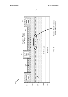
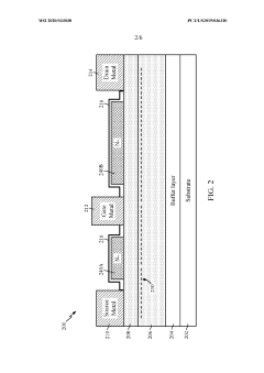
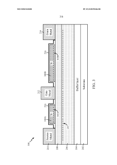
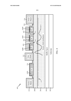
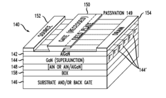
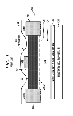
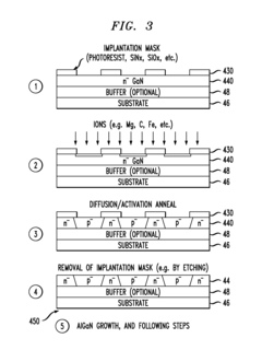
Gallium nitride high electron mobility transistor with ledges and field plates
PatentWO2020033038A1
Innovation
- Incorporating n-doped protuberances, or ledges, between the gate and source/drain electrodes, and optionally using field plates, to reduce surface states and increase channel electron density, thereby enhancing breakdown voltage and switching efficiency.
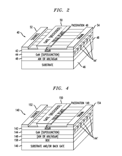
Gallium nitride superjunction devices
PatentInactiveUS20130240951A1
Innovation
- Incorporating a doped gallium nitride superjunction layer with a plurality of p/n junctions between the substrate and a barrier layer, which suppresses breakdown by modifying the electric field distribution, allowing for higher breakdown voltages and enabling the use of low-cost Si substrates.
Thermal Management Strategies for GaN HEMT Inverters
Effective thermal management is critical for GaN HEMT-based photovoltaic inverters as these devices generate significant heat during operation, particularly at high switching frequencies. The superior thermal conductivity of GaN compared to silicon provides an inherent advantage, but dedicated thermal management strategies remain essential to maximize efficiency and reliability.
Direct substrate cooling represents one of the most effective approaches, where the GaN HEMT die is mounted directly onto highly thermally conductive materials such as copper or aluminum nitride. This technique minimizes thermal resistance between the heat source and heat sink, enabling rapid heat dissipation. Advanced implementations incorporate microchannels beneath the substrate for liquid cooling, achieving thermal resistances below 0.1°C/W.
Advanced packaging technologies also play a crucial role in thermal management. Double-sided cooling configurations, where heat is extracted from both the top and bottom of the device, have demonstrated up to 40% improvement in thermal performance compared to conventional single-sided approaches. Additionally, embedded heat pipe solutions integrated within the module packaging provide passive, high-efficiency heat transfer without requiring additional power.
Active cooling systems utilizing intelligent thermal management controllers represent the cutting edge for high-power applications. These systems dynamically adjust cooling parameters based on real-time temperature monitoring, optimizing the balance between cooling performance and system efficiency. Machine learning algorithms are increasingly being deployed to predict thermal behavior and preemptively adjust cooling parameters before thermal issues arise.
Novel composite materials with tailored thermal properties are emerging as key enablers for next-generation thermal management. Diamond-copper composites, with thermal conductivity exceeding 600 W/mK, offer nearly twice the heat dissipation capability of pure copper. Similarly, graphene-enhanced thermal interface materials reduce contact resistance between components, addressing a critical bottleneck in thermal pathways.
System-level thermal design considerations are equally important, with computational fluid dynamics modeling enabling optimized heatsink geometries and airflow patterns. Distributed thermal management approaches, where heat generation is strategically spread across larger areas, prevent the formation of hotspots that can trigger thermal runaway and premature device failure.
The integration of these thermal management strategies must be considered early in the inverter design process rather than as an afterthought. This holistic approach ensures that GaN HEMT-based photovoltaic inverters can fully leverage the inherent efficiency advantages of wide-bandgap semiconductors while maintaining reliable operation across diverse environmental conditions and load profiles.
Cost-Performance Analysis of GaN vs Silicon Technologies
When comparing GaN (Gallium Nitride) and Silicon technologies for photovoltaic inverter applications, a comprehensive cost-performance analysis reveals significant trade-offs that manufacturers and system designers must consider. GaN HEMTs (High Electron Mobility Transistors) command a premium price point, typically 2-3 times higher than equivalent silicon MOSFETs or IGBTs on a per-component basis. This price differential stems from newer manufacturing processes, lower production volumes, and specialized packaging requirements for GaN devices.
However, the performance advantages of GaN often justify this higher initial component cost. GaN-based inverters demonstrate efficiency improvements of 1-3% over silicon alternatives, which translates to substantial energy savings over the lifetime of a photovoltaic system. A typical 100kW commercial installation using GaN inverters can generate additional revenue of $1,000-3,000 annually through increased energy production, potentially offsetting the higher initial investment within 2-4 years.
The system-level economics become even more favorable when considering the reduced cooling requirements and smaller passive components enabled by GaN's higher switching frequencies. GaN inverters typically require 30-50% smaller heatsinks and filter components, reducing overall material costs and improving power density by up to 3x compared to silicon-based designs. This translates to lower installation costs, reduced shipping expenses, and more efficient use of space.
Manufacturing complexity presents another important consideration. While silicon manufacturing processes have been optimized over decades, GaN production still faces yield challenges and requires specialized handling. This contributes to higher component costs but is gradually improving as manufacturers scale production and refine processes. Current industry projections suggest GaN component prices may decrease by 10-15% annually over the next five years as production volumes increase.
Reliability data increasingly supports GaN's long-term value proposition. Despite initial concerns about the maturity of GaN technology, field data now demonstrates comparable or superior reliability metrics compared to silicon alternatives when properly implemented. This reduces lifetime maintenance costs and improves system availability, further enhancing the economic case for GaN adoption in photovoltaic applications.
The total cost of ownership analysis increasingly favors GaN technology, particularly for new installations where the efficiency gains, reduced cooling requirements, and higher power density can be fully leveraged in the system design. For retrofit applications, the cost-benefit analysis remains more nuanced and depends heavily on specific installation parameters and energy pricing models.
Unlock deeper insights with Patsnap Eureka Quick Research — get a full tech report to explore trends and direct your research. Try now!
Generate Your Research Report Instantly with AI Agent
Supercharge your innovation with Patsnap Eureka AI Agent Platform!