

GaN HEMTs In Aerospace Power Electronics Systems
SEP 5, 20259 MIN READ
Generate Your Research Report Instantly with AI Agent
PatSnap Eureka helps you evaluate technical feasibility & market potential.
GaN HEMTs Evolution and Aerospace Applications
Gallium Nitride High Electron Mobility Transistors (GaN HEMTs) have undergone remarkable evolution since their inception in the early 1990s. The initial development focused on addressing the limitations of silicon-based power electronics, particularly in high-temperature and high-frequency applications. By the early 2000s, researchers had successfully demonstrated GaN HEMTs with breakdown voltages exceeding 1000V, marking a significant milestone in power electronics capability.
The evolution trajectory accelerated around 2010 when commercial entities began mass-producing GaN HEMTs for telecommunications and radar applications. This period saw substantial improvements in device reliability, with mean time to failure extending from thousands to millions of hours, enabling consideration for aerospace applications where reliability is paramount.
Between 2010-2015, a critical evolutionary phase occurred with the development of enhancement-mode GaN HEMTs (E-mode), overcoming the normally-on limitation of early devices. This advancement significantly simplified driver circuits and improved system safety, particularly crucial for aerospace power systems where fail-safe operation is essential.
The aerospace sector began serious adoption of GaN technology around 2015, initially in satellite communications systems where the reduced size and weight offered compelling advantages. The radiation hardness of GaN, superior to silicon by orders of magnitude, further accelerated adoption in space applications where radiation exposure presents significant challenges to semiconductor performance.
Recent evolutionary developments have focused on thermal management innovations, with diamond substrate integration emerging as a promising approach to address the high power density challenges. Advanced packaging techniques specifically designed for aerospace environments have enabled GaN HEMTs to withstand extreme temperature cycling, vacuum conditions, and mechanical stress during launch.
In current aerospace applications, GaN HEMTs have revolutionized power conversion systems, enabling up to 40% reduction in weight compared to silicon-based alternatives. This translates directly to fuel savings and increased payload capacity. Modern aircraft power distribution systems operating at higher voltages (270V DC and 540V DC) leverage GaN's high breakdown field strength to achieve unprecedented efficiency levels exceeding 98%.
The most recent evolutionary milestone involves the integration of GaN HEMTs with advanced digital control systems, creating intelligent power modules capable of real-time adaptation to changing mission profiles and environmental conditions. These systems can dynamically optimize efficiency based on flight phase, extending the operational range of electric propulsion systems in next-generation aircraft designs.
Aerospace Power Electronics Market Analysis
The aerospace power electronics market is experiencing robust growth, driven by increasing demand for more electric aircraft (MEA) architectures and advanced satellite systems. Current market valuation stands at approximately 2.8 billion USD, with projections indicating a compound annual growth rate of 6.7% through 2030. This growth trajectory is primarily fueled by the global push toward fuel-efficient aircraft and the expanding space exploration initiatives by both governmental agencies and private enterprises.
The market segmentation reveals distinct application areas where GaN HEMTs are gaining traction. Power conversion systems represent the largest segment, accounting for nearly 40% of the market share, followed by motor drives, battery management systems, and actuation systems. Geographically, North America dominates with roughly 45% market share, benefiting from substantial defense budgets and the presence of major aerospace manufacturers. Europe follows at 30%, with Asia-Pacific emerging as the fastest-growing region due to increasing investments in aerospace infrastructure.
Customer requirements in aerospace power electronics are evolving rapidly, with emphasis on higher power density, improved thermal management, radiation hardness, and reliability under extreme conditions. The demand for systems capable of operating at higher temperatures (beyond 200°C) and withstanding radiation effects in space applications has created a significant market opportunity for wide-bandgap semiconductors like GaN HEMTs.
Industry trends indicate a shift toward higher voltage systems (>1kV) to reduce weight and improve efficiency in aircraft electrical systems. The satellite market segment is particularly promising for GaN technology, with small satellite constellations requiring compact, efficient power electronics solutions. The commercial aviation sector's recovery post-pandemic has accelerated the adoption of next-generation power electronic systems, with major aircraft manufacturers incorporating more electric systems in their designs.
Market barriers include stringent certification requirements, long qualification cycles (typically 3-5 years), and high reliability standards that slow down technology adoption. The cost premium of GaN-based solutions compared to traditional silicon remains a challenge, though this gap is narrowing as manufacturing processes mature and economies of scale improve.
Competitive dynamics show increasing collaboration between semiconductor manufacturers and aerospace system integrators to develop customized GaN solutions. The supply chain is evolving to accommodate the specialized requirements of aerospace-grade GaN devices, with emphasis on traceability, quality control, and long-term availability guarantees that are essential for aerospace programs with lifecycles extending over decades.
GaN HEMTs Technical Challenges in Aerospace
GaN HEMTs face significant technical challenges in aerospace applications despite their promising performance characteristics. The harsh operating environment of aerospace systems imposes extreme temperature variations, from cryogenic conditions during high-altitude flight to temperatures exceeding 300°C in power electronics systems. These thermal extremes stress device reliability and accelerate degradation mechanisms, particularly affecting gate leakage currents and threshold voltage stability.
Radiation hardness presents another critical challenge, as aerospace electronics are exposed to cosmic rays, solar flares, and trapped radiation belts. GaN HEMTs exhibit varying responses to different radiation types, with displacement damage and ionization effects potentially causing parametric shifts and catastrophic failures. Current radiation hardening techniques often compromise device performance, creating difficult design trade-offs.
Reliability concerns are paramount in aerospace applications where maintenance is impossible after deployment. GaN HEMTs suffer from several degradation mechanisms including hot electron effects, inverse piezoelectric effects, and time-dependent dielectric breakdown. These failure modes are exacerbated by the high-voltage, high-frequency operation typical in aerospace power systems, necessitating comprehensive reliability testing protocols that can accurately predict device lifetime under mission-specific conditions.
Thermal management represents a significant engineering challenge due to the high power densities in GaN devices. In aerospace systems, where size and weight are strictly constrained, conventional cooling solutions prove inadequate. Advanced thermal management techniques including diamond substrates, microfluidic cooling channels, and phase-change materials are being explored, but each introduces manufacturing complexities and reliability concerns.
Integration challenges persist when incorporating GaN HEMTs into aerospace systems. The high switching speeds generate electromagnetic interference (EMI) that can affect sensitive navigation and communication equipment. Additionally, gate driver circuits must be carefully designed to handle the fast switching transients while maintaining isolation in the high-voltage environment typical of aerospace power systems.
Manufacturing consistency and yield remain problematic for space-grade GaN HEMTs. Wafer-to-wafer and run-to-run variations affect device performance parameters, while defect densities in the epitaxial layers impact long-term reliability. The aerospace industry's stringent qualification requirements, including MIL-STD-883 and JEDEC standards, present significant barriers to widespread adoption, as qualification processes can take years to complete and require substantial investment.
Cost factors further complicate GaN HEMT adoption in aerospace applications. The specialized manufacturing processes, extensive qualification testing, and low production volumes result in significantly higher costs compared to silicon alternatives, challenging the business case for GaN technology despite its technical advantages.
Current GaN HEMTs Implementation in Aerospace Systems
01 GaN HEMT device structures and fabrication
Various structural designs and fabrication methods for GaN HEMTs, including layer compositions, gate configurations, and manufacturing processes. These innovations focus on improving device performance, reliability, and yield through optimized epitaxial structures, novel gate designs, and advanced processing techniques that enhance electron mobility and power handling capabilities.- GaN HEMT device structures and fabrication methods: Various structural designs and fabrication techniques for GaN HEMTs are disclosed, including layer compositions, gate configurations, and manufacturing processes. These innovations focus on optimizing the device architecture to enhance performance characteristics such as power handling, switching speed, and reliability. Key structural elements include buffer layers, barrier layers, gate designs, and surface passivation techniques that collectively determine the device's electrical properties.
- Power electronics applications of GaN HEMTs: GaN HEMTs are implemented in various power electronic applications, including power converters, amplifiers, and switching circuits. These transistors offer advantages such as high breakdown voltage, low on-resistance, and high-frequency operation, making them suitable for efficient power management systems. The implementations include circuit designs that leverage GaN HEMT characteristics for improved power density and thermal performance in applications ranging from consumer electronics to industrial power systems.
- Thermal management and reliability enhancement: Techniques for improving the thermal performance and reliability of GaN HEMTs are presented, addressing challenges such as self-heating effects and degradation mechanisms. These approaches include advanced packaging solutions, heat dissipation structures, and materials engineering to maintain device performance under high-power operation. Reliability enhancement methods focus on mitigating electron trapping, current collapse, and other phenomena that affect long-term stability.
- Integration and packaging technologies: Integration and packaging solutions for GaN HEMTs are developed to optimize their performance in practical applications. These include monolithic integration with other semiconductor devices, advanced interconnect technologies, and novel packaging approaches that minimize parasitic effects. The integration strategies enable compact system designs while addressing thermal management and electromagnetic interference challenges, facilitating the adoption of GaN HEMTs in diverse electronic systems.
- Performance enhancement techniques: Various methods to enhance the performance of GaN HEMTs are disclosed, including surface treatments, novel material combinations, and structural modifications. These techniques aim to improve key parameters such as transconductance, breakdown voltage, and frequency response. Approaches include field plate designs, gate engineering, channel modifications, and novel dielectric materials that collectively optimize the balance between conduction efficiency and breakdown strength for specific application requirements.
02 Power management and efficiency improvements
Techniques for enhancing power efficiency and management in GaN HEMT devices, including circuit designs that optimize power conversion, reduce losses, and improve thermal performance. These innovations address challenges in high-frequency power applications by implementing novel switching methodologies, driver circuits, and power distribution networks that maximize the inherent advantages of GaN technology.Expand Specific Solutions03 Thermal management solutions
Methods and structures for managing heat dissipation in GaN HEMTs, which is critical for maintaining device performance and reliability. These solutions include innovative substrate materials, heat spreading techniques, packaging designs, and thermal interface materials that effectively remove heat from the active device regions during high-power operation.Expand Specific Solutions04 Reliability enhancement techniques
Approaches to improve the long-term reliability and operational stability of GaN HEMTs under various stress conditions. These techniques address common failure mechanisms such as current collapse, gate leakage, and electron trapping through passivation layers, buffer designs, field plates, and stress testing methodologies that extend device lifetime and maintain consistent performance.Expand Specific Solutions05 Integration and application-specific designs
Specialized GaN HEMT designs optimized for specific applications such as RF amplifiers, power converters, and integrated circuits. These innovations focus on system-level integration, monolithic implementation, and application-specific performance enhancements that leverage the high-frequency, high-voltage capabilities of GaN technology in practical electronic systems.Expand Specific Solutions
Leading GaN Semiconductor Manufacturers and Aerospace Integrators
The GaN HEMTs aerospace power electronics market is in a growth phase, with increasing adoption driven by demands for higher efficiency and power density in harsh environments. The market is expanding at approximately 15-20% annually, reaching an estimated $250-300 million in aerospace applications. Leading players include Wolfspeed, which dominates with advanced GaN-on-SiC technology, Northrop Grumman with defense-focused solutions, and MACOM offering commercial aerospace applications. Other significant competitors include HRL Laboratories, Qualcomm, and Huawei, who are investing in GaN HEMT R&D. The technology has reached moderate maturity for lower power applications but continues evolving for high-reliability aerospace systems, with university collaborations (Cornell, HKUST) accelerating innovation in thermal management and radiation hardening.
Wolfspeed, Inc.
Technical Solution: Wolfspeed has developed advanced GaN HEMT technology specifically optimized for aerospace power electronics systems. Their solution features high-frequency operation (up to 100 MHz) with power densities exceeding 5 kW/in³, enabling significant size and weight reduction critical for aerospace applications. Wolfspeed's GaN-on-SiC technology demonstrates superior thermal conductivity (>3.5 W/cm·K) compared to traditional silicon-based solutions, allowing for efficient heat dissipation in the harsh aerospace environment. Their devices operate reliably at junction temperatures up to 225°C with breakdown voltages exceeding 1200V, making them suitable for high-altitude operation. Wolfspeed has implemented advanced packaging techniques with low parasitic inductance (<2nH) to maximize switching performance and reliability under extreme conditions. Their aerospace-grade GaN HEMTs undergo rigorous radiation hardness testing and qualification to MIL-STD-883 standards, ensuring long-term reliability in space applications.
Strengths: Industry-leading thermal performance and power density; extensive radiation hardness qualification; proven reliability in extreme environments. Weaknesses: Higher cost compared to silicon alternatives; requires specialized design considerations for optimal performance; limited standardization across aerospace platforms.
Northrop Grumman Systems Corp.
Technical Solution: Northrop Grumman has developed proprietary GaN HEMT technology specifically engineered for aerospace power electronics systems with a focus on radiation hardness and reliability. Their solution incorporates advanced epitaxial layer structures with optimized AlGaN/GaN interfaces that demonstrate superior electron mobility (>2000 cm²/V·s) and channel density. Northrop's aerospace GaN HEMTs feature specialized field plates and edge termination designs that enable operation at voltages exceeding 900V while maintaining leakage currents below 10μA/mm². The company has implemented proprietary surface passivation techniques to mitigate electron trapping effects, resulting in minimal RF-DC dispersion even after exposure to radiation doses exceeding 1 Mrad. Their devices demonstrate exceptional reliability with MTTF exceeding 10⁷ hours at 175°C channel temperature, critical for long-duration space missions. Northrop Grumman's GaN technology has been integrated into compact, radiation-hardened power converters achieving efficiencies above 96% at switching frequencies up to 5 MHz, enabling significant SWaP (Size, Weight, and Power) improvements in satellite and aircraft power systems.
Strengths: Exceptional radiation hardness specifically designed for space applications; proven reliability in extreme aerospace environments; vertical integration of design, manufacturing and testing capabilities. Weaknesses: Primarily focused on defense/government applications with limited commercial availability; higher cost structure compared to commercial alternatives; proprietary technology with potential integration challenges.
Critical Patents and Research in GaN Power Electronics
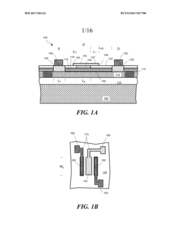
High-voltage GAN high electron mobility transistors
PatentWO2017181121A2
Innovation
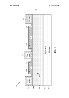
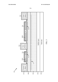
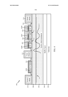
- The development of high-voltage HEMTs with a gallium-nitride material structure, including a buffer layer, conduction layer, barrier layer, gate, source, and drain, with a gate-connected field plate extending beyond the gate edges, and a thin gallium-oxide layer formed through oxygen plasma treatment, to enhance reverse-bias voltage withstand and reduce leakage currents.

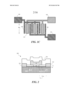
Gallium nitride high electron mobility transistor with ledges and field plates
PatentWO2020033038A1
Innovation
- Incorporating n-doped protuberances, or ledges, between the gate and source/drain electrodes, and optionally using field plates, to reduce surface states and increase channel electron density, thereby enhancing breakdown voltage and switching efficiency.
Radiation Hardening Techniques for Aerospace GaN Devices
Radiation hardening techniques for GaN HEMTs in aerospace applications have evolved significantly in response to the harsh radiation environments encountered in space missions. These techniques can be broadly categorized into process-level hardening, device-level hardening, and system-level hardening approaches, each addressing specific vulnerability mechanisms.
Process-level radiation hardening focuses on material engineering and fabrication techniques to enhance the intrinsic radiation tolerance of GaN devices. This includes the development of high-purity epitaxial layers with reduced defect densities, which minimize charge trapping sites that can be activated by radiation. Advanced substrate materials such as silicon carbide (SiC) provide improved thermal conductivity and reduced lattice mismatch, contributing to enhanced radiation resilience.
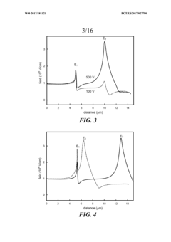
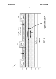
Device-level hardening techniques involve specific design modifications to mitigate radiation effects. Field plate structures have proven particularly effective in redistributing electric fields and reducing hot electron effects that can be exacerbated by radiation exposure. Gate recess engineering and passivation layer optimization are employed to minimize surface-related trapping phenomena that contribute to threshold voltage shifts under radiation.
Multiple gate architectures represent another significant advancement, where redundant gate structures ensure continued functionality even if one gate experiences radiation-induced damage. T-gate and Γ-gate geometries have demonstrated superior radiation tolerance compared to conventional gate designs by reducing gate leakage currents post-irradiation.
System-level radiation hardening incorporates redundancy, shielding, and intelligent power management. Triple modular redundancy (TMR) configurations enable fault-tolerant operation by implementing voting mechanisms across multiple GaN power stages. Active compensation circuits continuously monitor device parameters and adjust operating conditions to counteract radiation-induced degradation effects.
Recent innovations include the development of radiation-aware control algorithms that dynamically adjust switching frequencies and duty cycles based on real-time radiation monitoring. These adaptive systems can extend device lifetime in variable radiation environments by reducing stress during periods of intense radiation.
Qualification testing protocols for aerospace GaN devices have become increasingly sophisticated, with combined environment testing that simultaneously evaluates thermal cycling, mechanical stress, and radiation exposure to more accurately predict in-orbit performance. Accelerated life testing under radiation has been standardized to enable meaningful comparison between different hardening approaches.
The effectiveness of these techniques has enabled GaN HEMTs to achieve total ionizing dose (TID) tolerance exceeding 1 Mrad(Si) and single event effect (SEE) immunity up to linear energy transfer (LET) values of 80 MeV·cm²/mg, making them suitable for even the most demanding aerospace missions.
Process-level radiation hardening focuses on material engineering and fabrication techniques to enhance the intrinsic radiation tolerance of GaN devices. This includes the development of high-purity epitaxial layers with reduced defect densities, which minimize charge trapping sites that can be activated by radiation. Advanced substrate materials such as silicon carbide (SiC) provide improved thermal conductivity and reduced lattice mismatch, contributing to enhanced radiation resilience.
Device-level hardening techniques involve specific design modifications to mitigate radiation effects. Field plate structures have proven particularly effective in redistributing electric fields and reducing hot electron effects that can be exacerbated by radiation exposure. Gate recess engineering and passivation layer optimization are employed to minimize surface-related trapping phenomena that contribute to threshold voltage shifts under radiation.
Multiple gate architectures represent another significant advancement, where redundant gate structures ensure continued functionality even if one gate experiences radiation-induced damage. T-gate and Γ-gate geometries have demonstrated superior radiation tolerance compared to conventional gate designs by reducing gate leakage currents post-irradiation.
System-level radiation hardening incorporates redundancy, shielding, and intelligent power management. Triple modular redundancy (TMR) configurations enable fault-tolerant operation by implementing voting mechanisms across multiple GaN power stages. Active compensation circuits continuously monitor device parameters and adjust operating conditions to counteract radiation-induced degradation effects.
Recent innovations include the development of radiation-aware control algorithms that dynamically adjust switching frequencies and duty cycles based on real-time radiation monitoring. These adaptive systems can extend device lifetime in variable radiation environments by reducing stress during periods of intense radiation.
Qualification testing protocols for aerospace GaN devices have become increasingly sophisticated, with combined environment testing that simultaneously evaluates thermal cycling, mechanical stress, and radiation exposure to more accurately predict in-orbit performance. Accelerated life testing under radiation has been standardized to enable meaningful comparison between different hardening approaches.
The effectiveness of these techniques has enabled GaN HEMTs to achieve total ionizing dose (TID) tolerance exceeding 1 Mrad(Si) and single event effect (SEE) immunity up to linear energy transfer (LET) values of 80 MeV·cm²/mg, making them suitable for even the most demanding aerospace missions.
Thermal Management Solutions for GaN Aerospace Applications
Thermal management represents a critical challenge in the deployment of GaN HEMTs in aerospace power electronics systems. The inherent high power density of GaN devices, while advantageous for performance, creates significant thermal challenges that must be addressed through specialized solutions tailored to the aerospace environment.
Advanced thermal interface materials (TIMs) have emerged as a primary solution pathway, with nano-enhanced composites showing particular promise. These materials, incorporating graphene, carbon nanotubes, and ceramic nanoparticles, demonstrate thermal conductivity values exceeding 25 W/m·K while maintaining the mechanical compliance necessary for aerospace applications where thermal cycling and vibration are common.
Direct liquid cooling technologies have evolved significantly for aerospace GaN applications, with single-phase and two-phase cooling systems being adapted to meet the stringent requirements of flight hardware. Dielectric coolants such as Fluorinert and Novec fluids enable direct chip cooling without electrical interference, achieving junction temperature reductions of 30-45°C compared to conventional approaches.
Microfluidic cooling channels integrated directly into GaN device packaging represent another innovative approach. These microscale cooling structures, fabricated using advanced manufacturing techniques, allow coolant flow in close proximity to the heat source. Recent implementations have demonstrated thermal resistances below 0.1°C·cm²/W, enabling power densities exceeding 1 kW/cm² while maintaining safe operating temperatures.
Advanced heat spreading technologies utilizing synthetic diamond, chemical vapor deposition (CVD) diamond films, and graphite-based materials offer thermal conductivity values 4-5 times higher than copper while providing significant weight advantages critical for aerospace applications. These materials effectively distribute heat from localized hotspots across larger areas for more efficient cooling.
Thermal management system integration presents unique challenges in aerospace environments. Solutions must address not only steady-state thermal performance but also transient thermal behavior during mission profiles. Adaptive cooling systems that modulate cooling capacity based on operational demands show particular promise, with recent flight demonstrations validating 15-20% improvements in overall system efficiency.
Reliability considerations remain paramount, with thermal solutions required to maintain performance across extreme temperature ranges (-55°C to +125°C), withstand radiation effects, and operate reliably in vacuum conditions. Qualification testing protocols specific to aerospace GaN thermal management have been developed, incorporating accelerated life testing methodologies that accurately predict long-term performance in these demanding environments.
Unlock deeper insights with PatSnap Eureka Quick Research — get a full tech report to explore trends and direct your research. Try now!
Generate Your Research Report Instantly with AI Agent
Supercharge your innovation with PatSnap Eureka AI Agent Platform!